
P-Type Metal Oxide Semiconductor Thin Films: Synthesis and Chemical Sensor Applications


Abstract
:1. Introduction
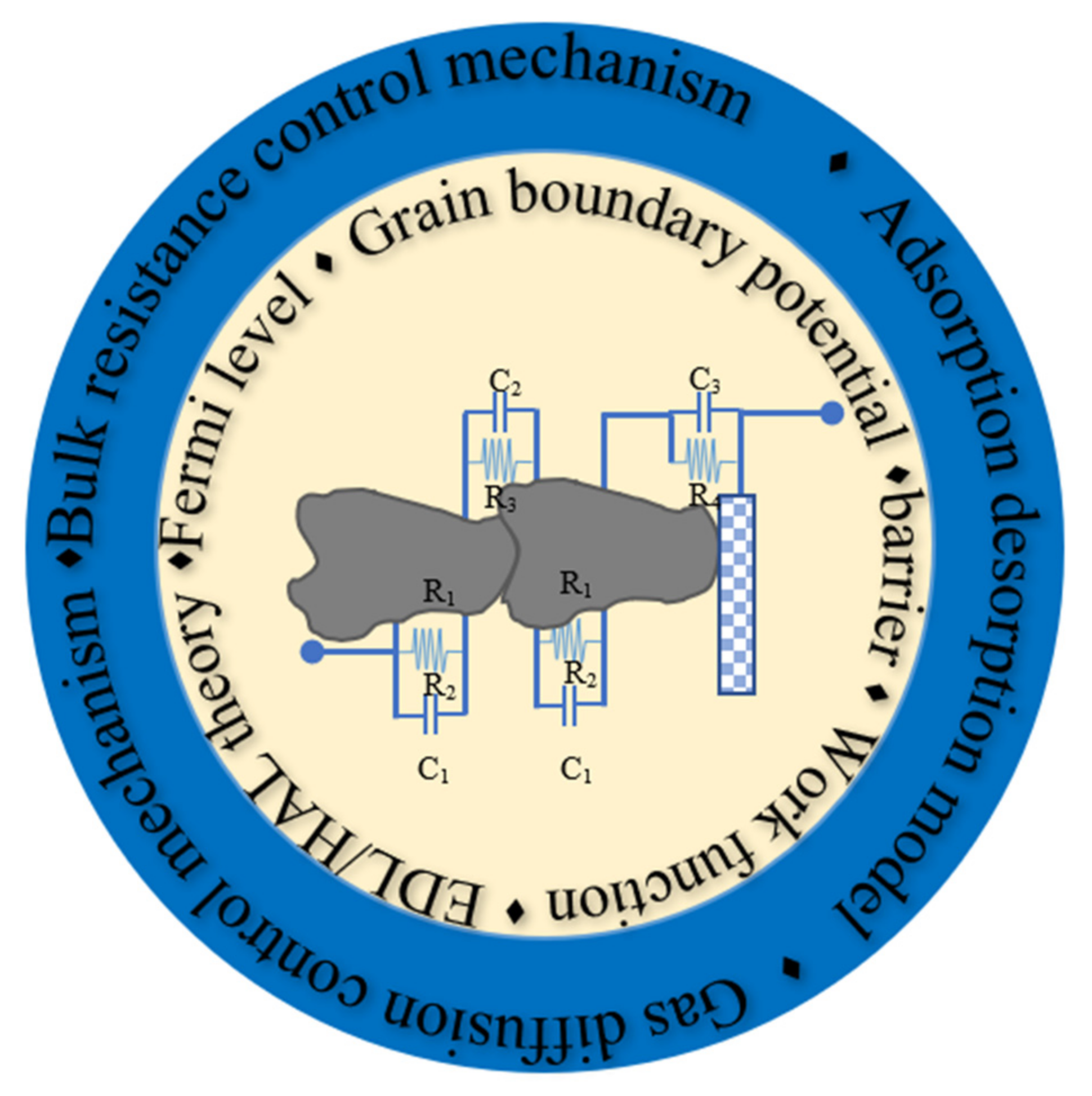
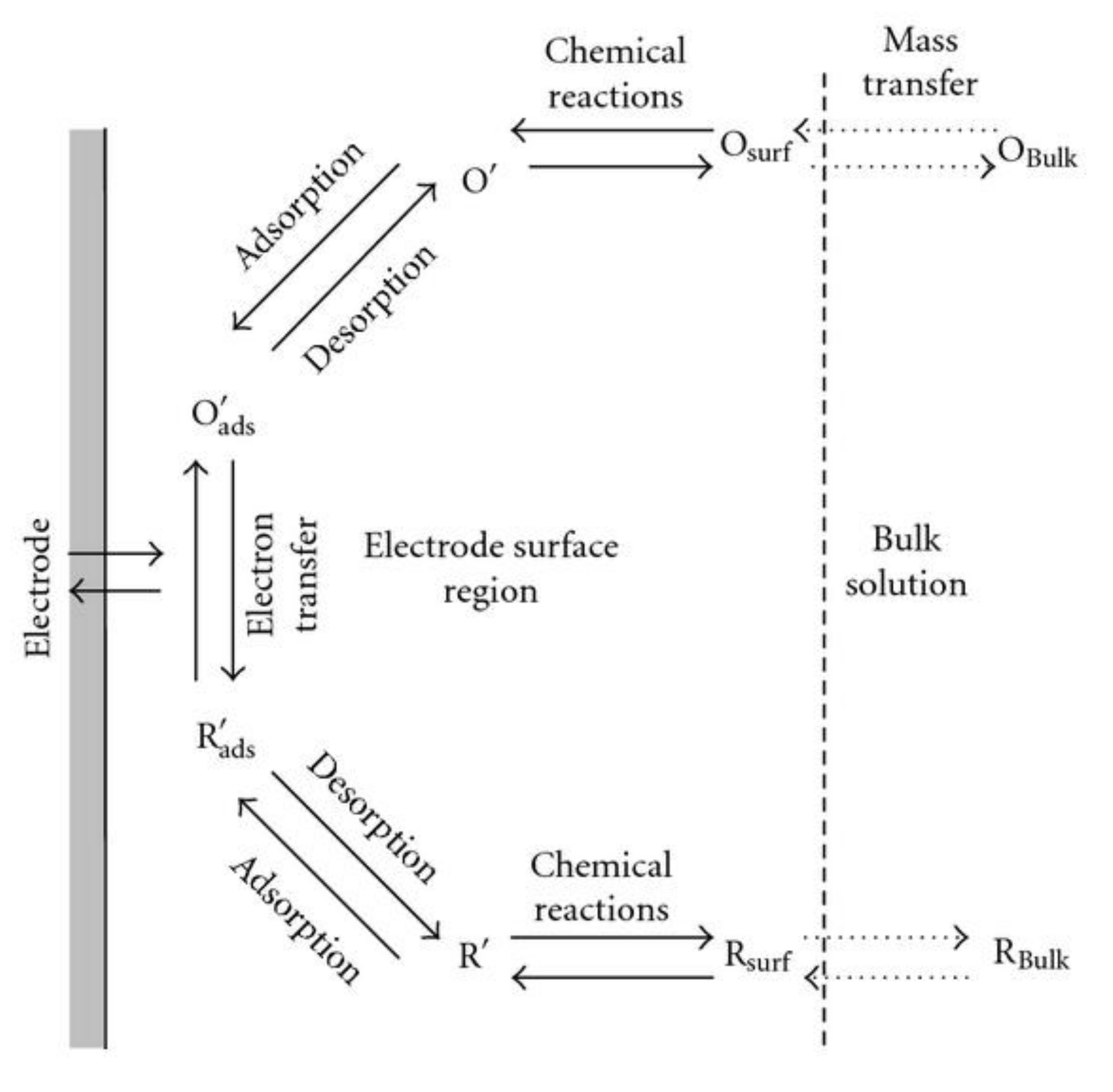
2. Mechanism of P-Type MOX Thin Films
3. Synthesis of P-Type MOX Thin Films
3.1. Vapor-Phase Growth Methods
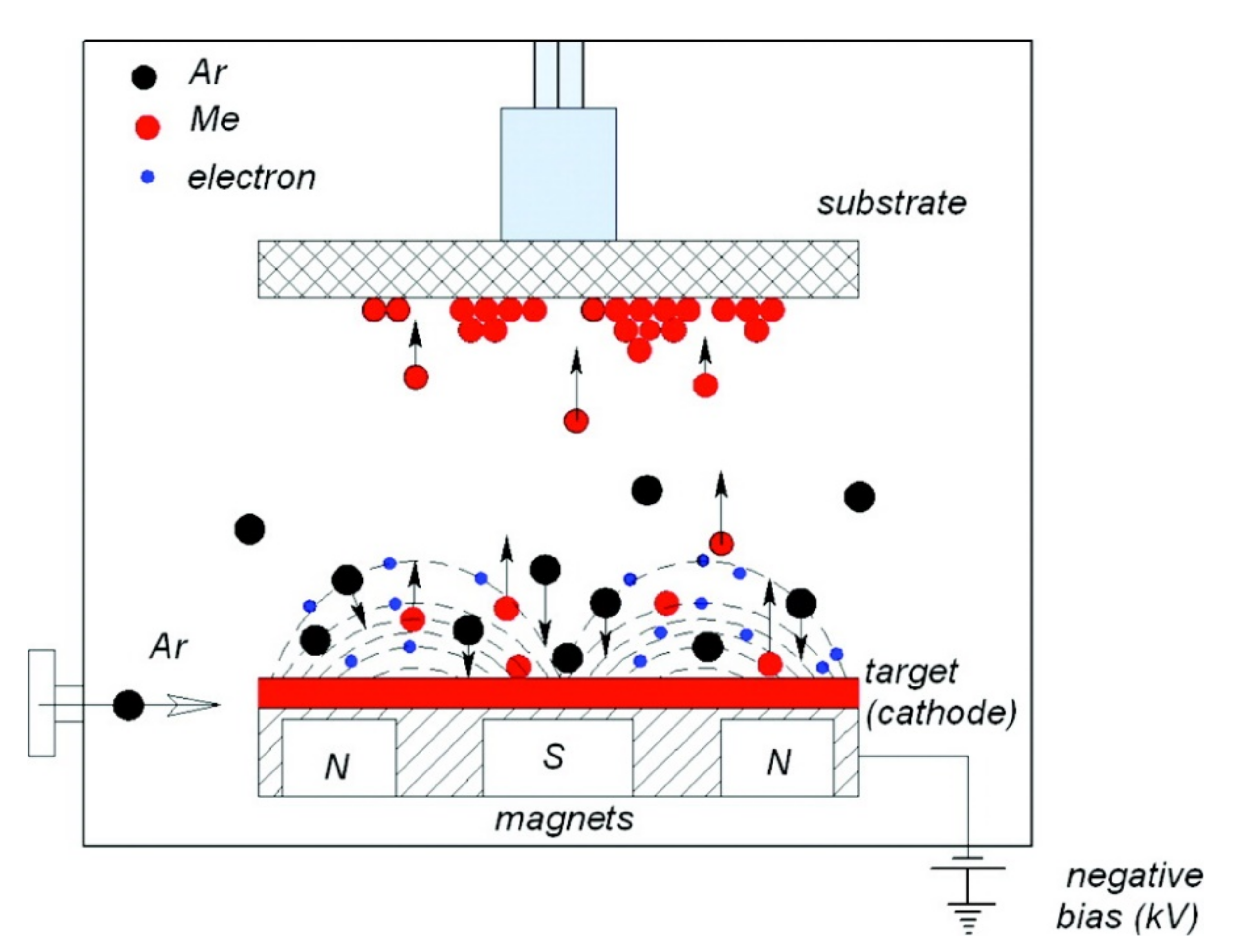
3.1.1. Magnetron Sputtering
3.1.2. Thermal Evaporation
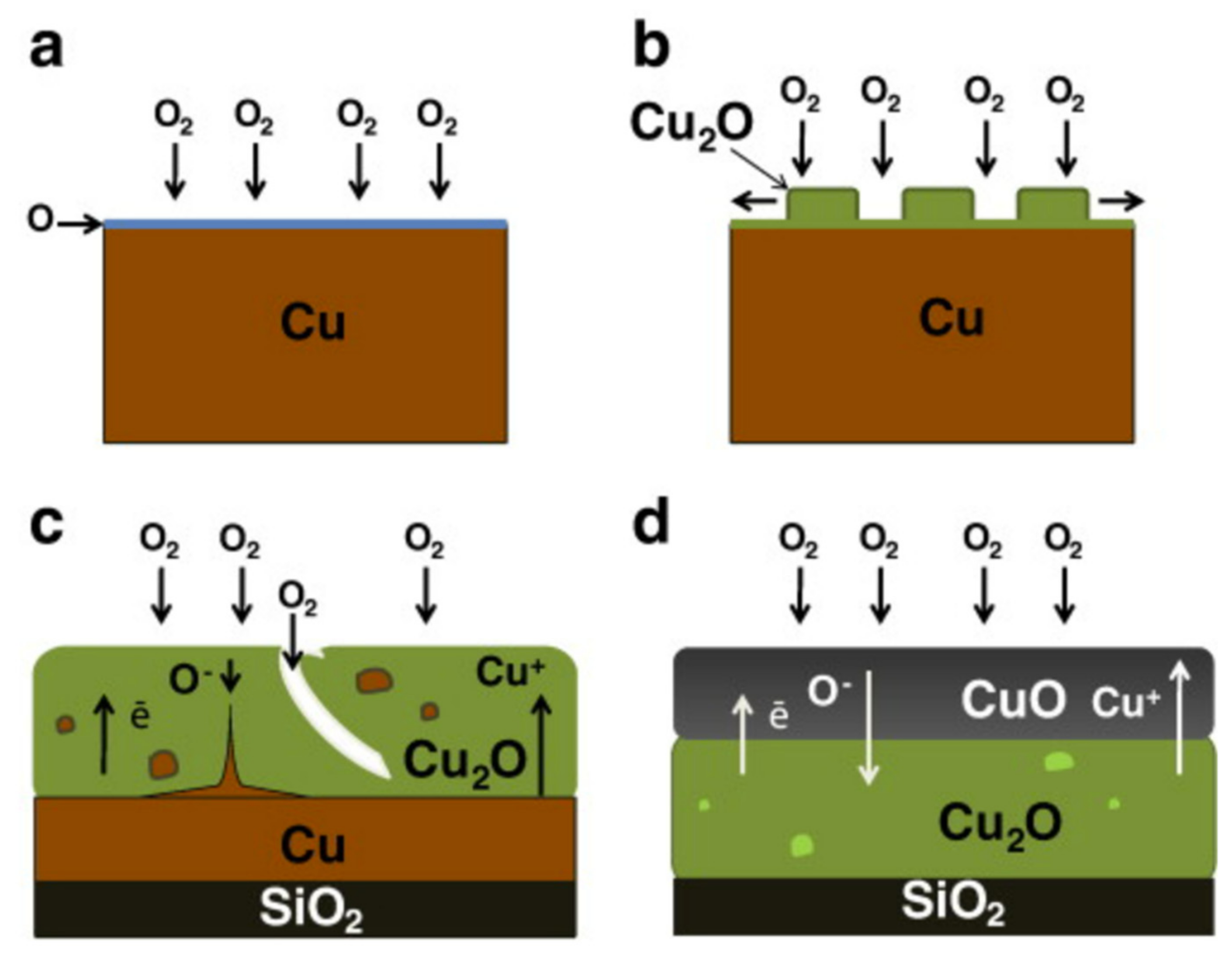
3.1.3. Thermal Oxidation
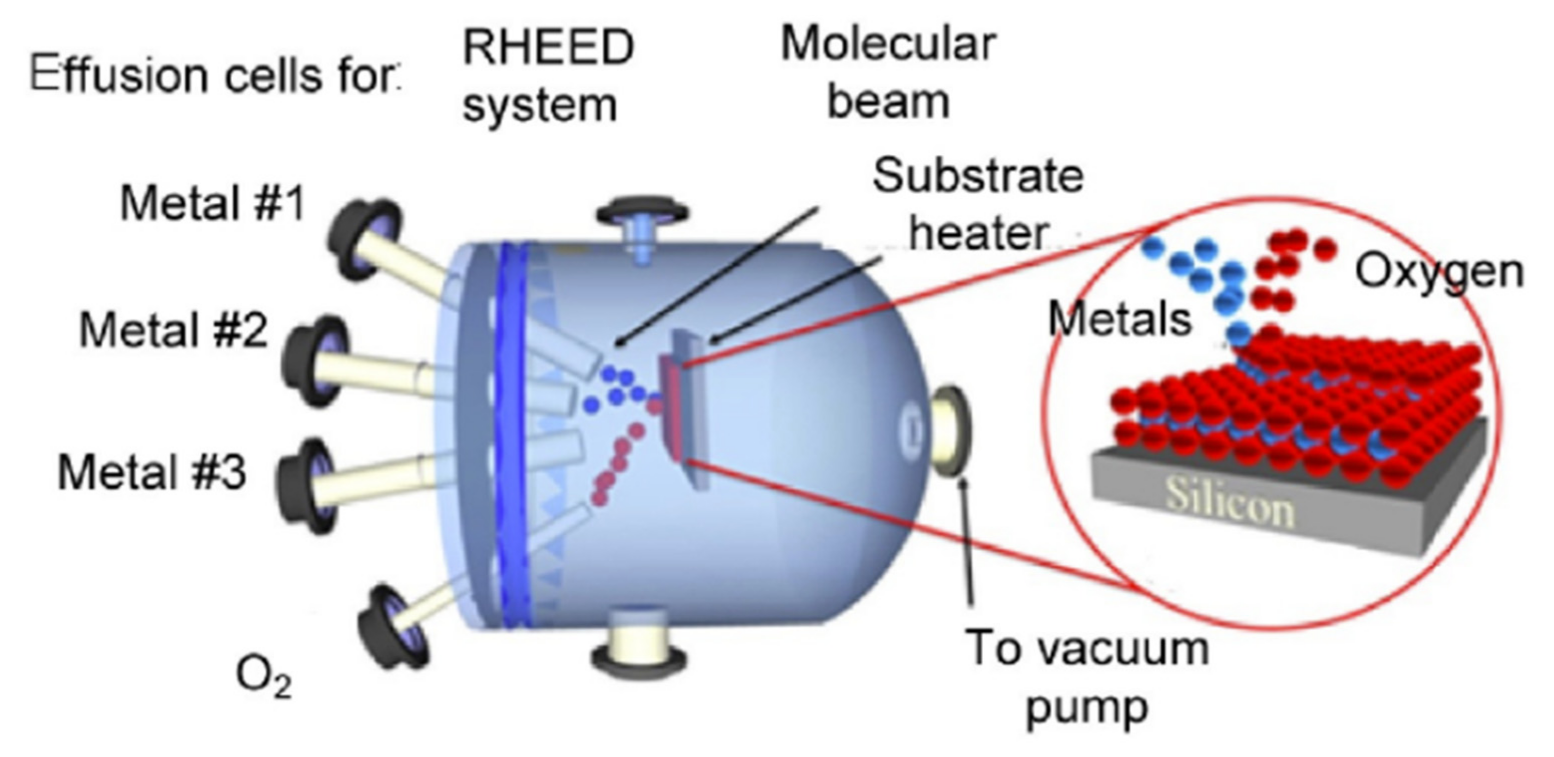
3.1.4. Molecular-Beam Epitaxy (MEB)
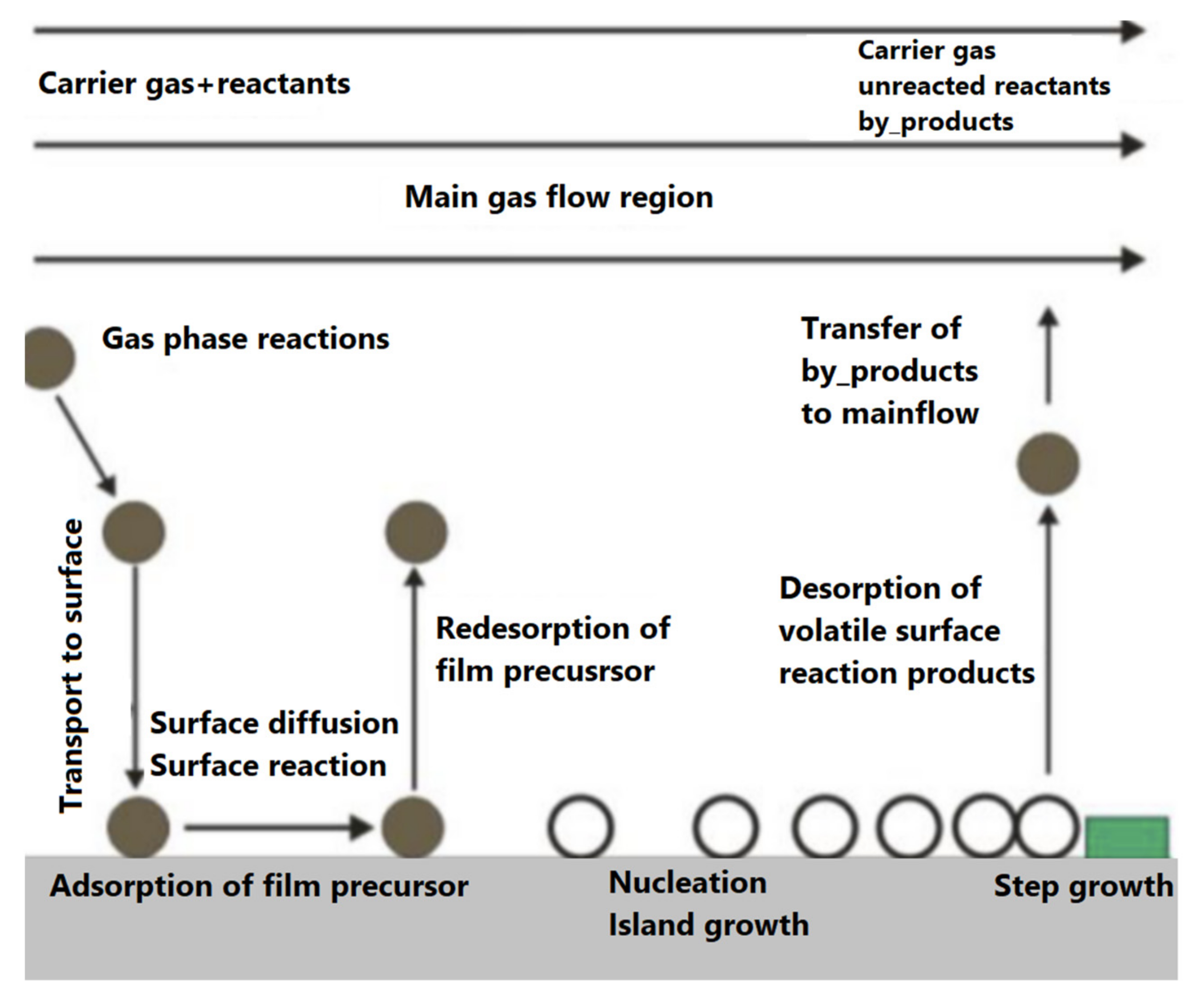
3.1.5. Chemical Vapor Deposition (CVD)
3.2. Liquid-Phase Route
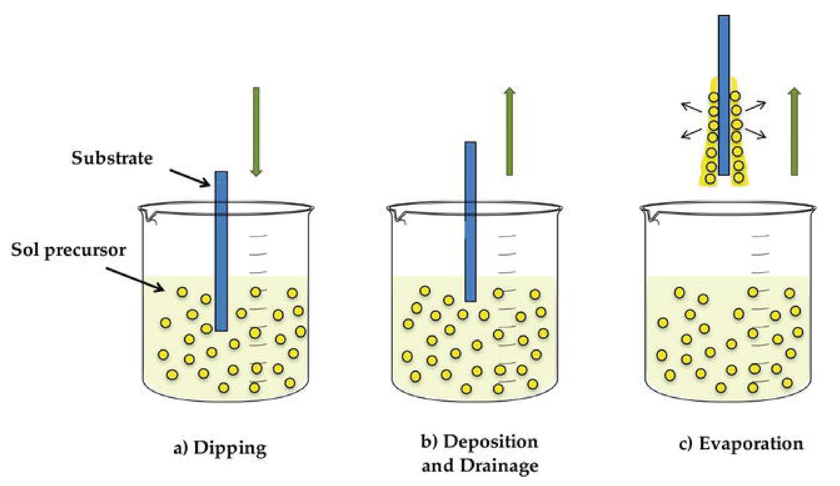
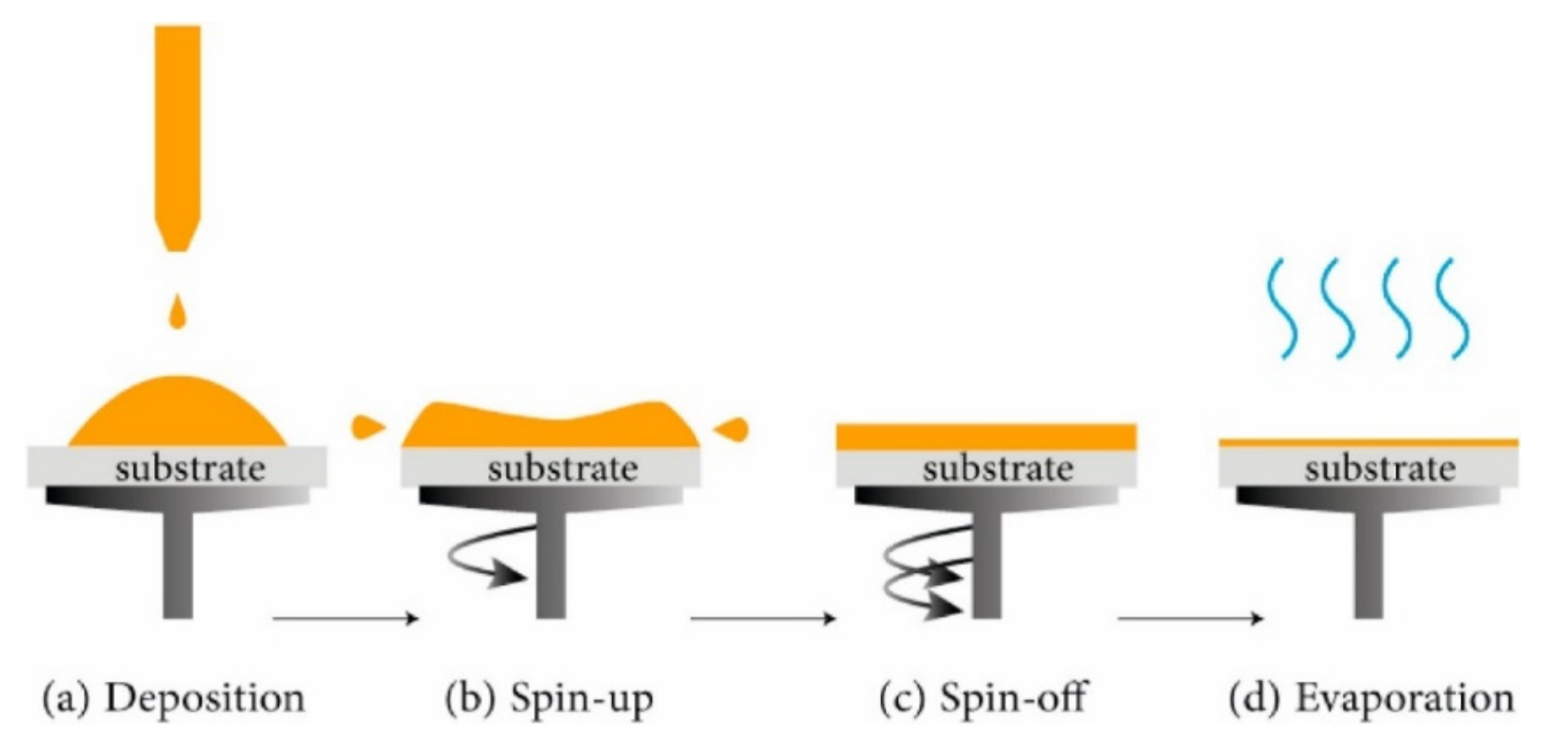
3.2.1. Sol–Gel
- 1.
- Synthesis of the ‘sol’ from hydrolysis and partial condensation of alkoxides.
- 2.
- Formation of the ‘gel’ via polycondensation to form metal–oxo–metal or metal–hydroxy–metal bonds.
- 3.
- Syneresis or ‘aging’, where condensation continues within the gel network, often shrinking it and resulting in expulsion of solvent.
- 4.
- Drying the gel either to form a dense ‘xerogel’ via collapse of the porous network or an aerogel, for example, through supercritical drying.
- 5.
- Removal of surface M–OH groups through calcination at high temperatures, up to 800 °C (if required).
- Spin Coating
- Dip Coating
- Immersion: the substrate is slowly dipped in the material precursor solution at a uniform speed.
- Pull-up: the substrate is kept inside the solution for a fixed short duration, and then slowly pulled up.
- Deposition: uniform deposition of thin layers on the substrate happens during the slow and steady pull-up stage. The withdrawal rate controls the layer thickness (faster pull-up results in thick layers).
- Drainage: excessive liquid contents are simultaneously drained from the substrate, beginning during the pull-up stage and continuing outside the solution.
- Evaporation: evaporation of solvent and formation of a thin layer happens. If the solvent is volatile (e.g., alcohol), evaporation begins during the pull-up stage and continues during the drainage sage.
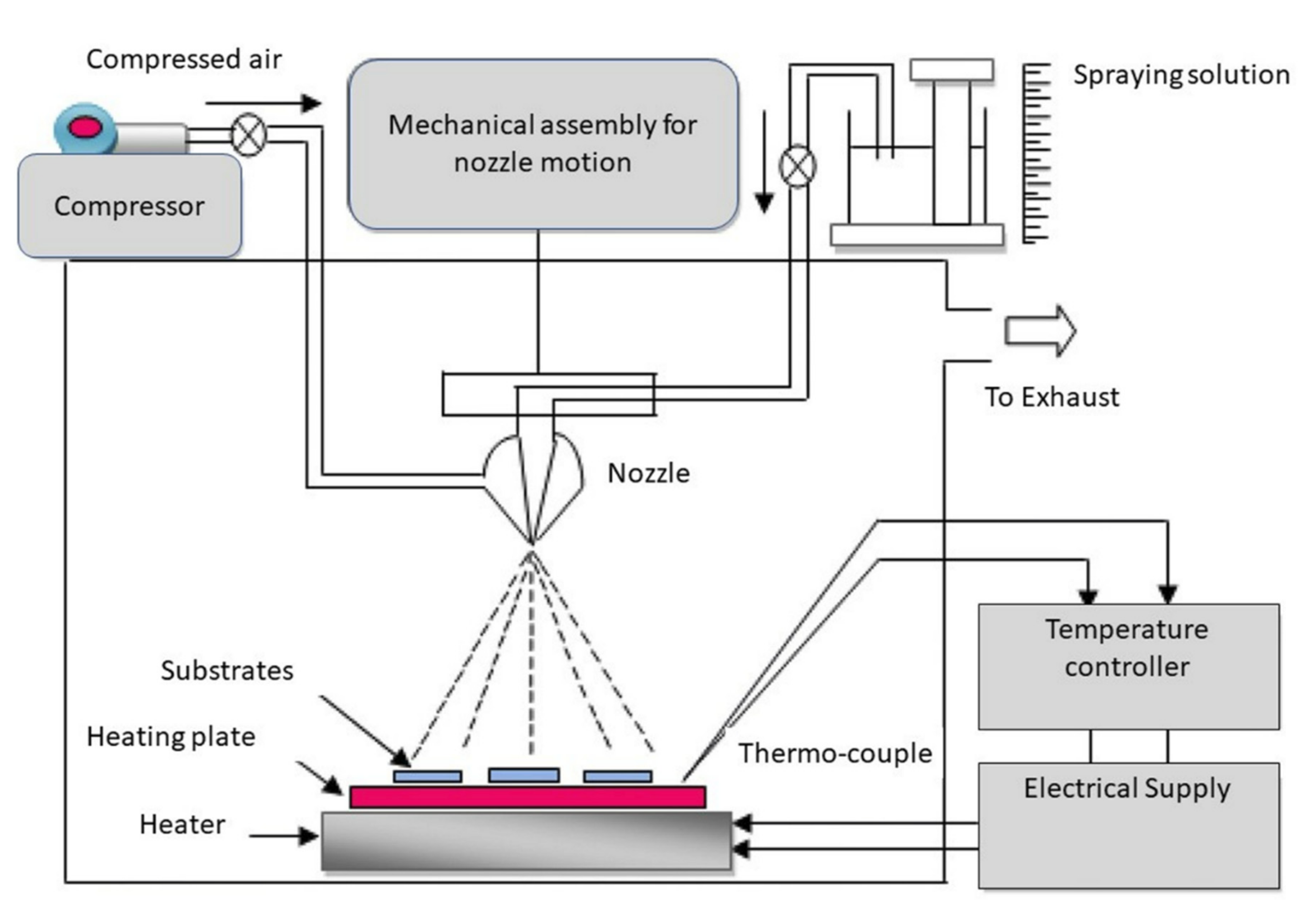
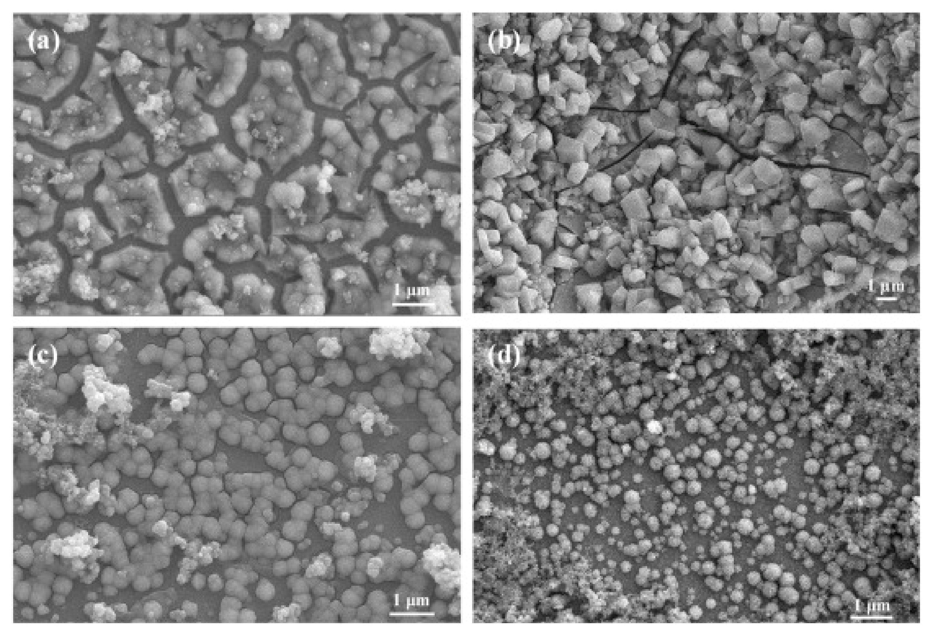
3.2.2. Spray Pyrolysis
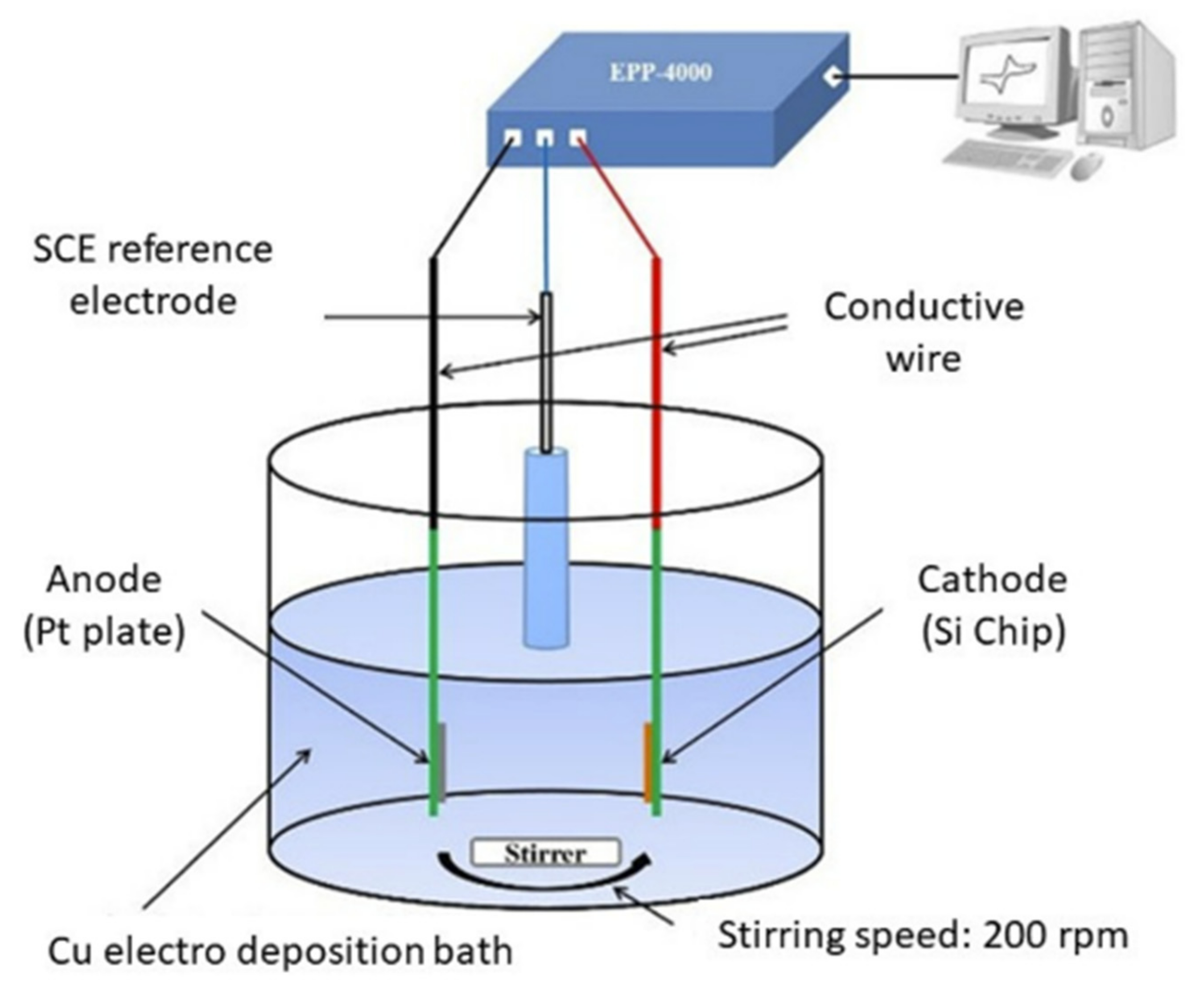
3.2.3. Electrodeposition
4. Sensing Properties of P-Type MOX Thin Films
4.1. Reducing Gases
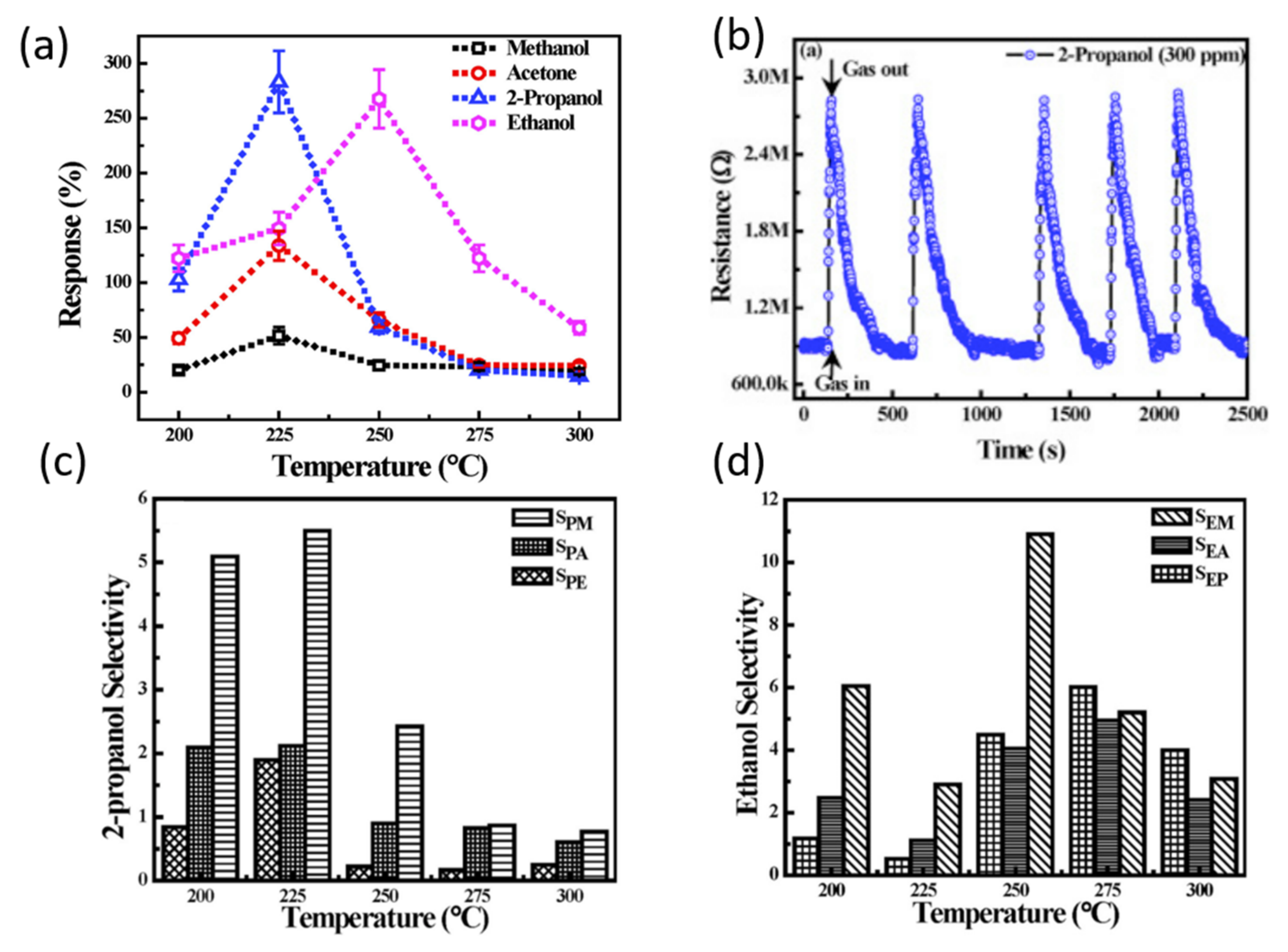
4.1.1. Volatile Organic Compounds (VOCs)
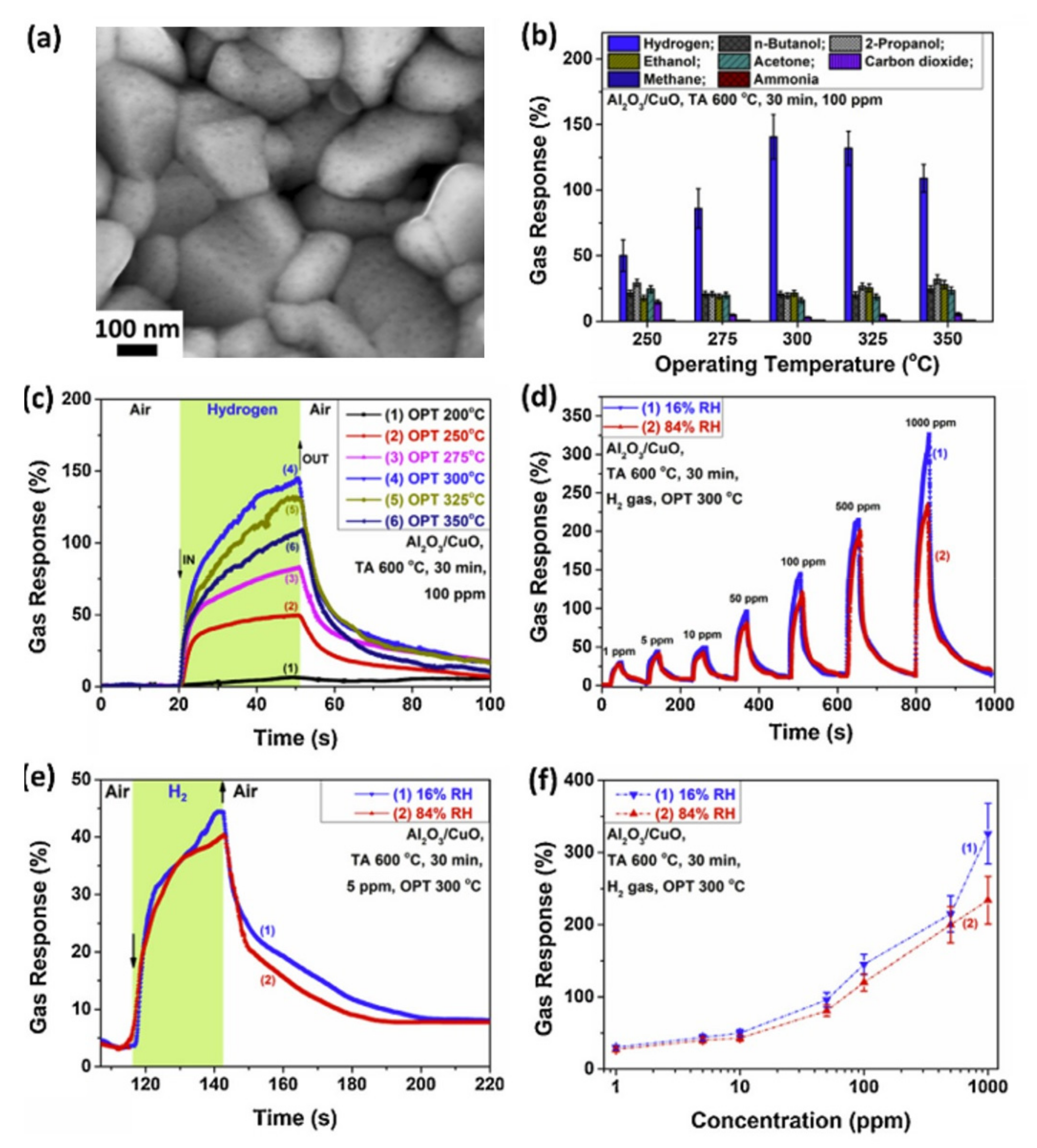
4.1.2. Hydrogen (H2)
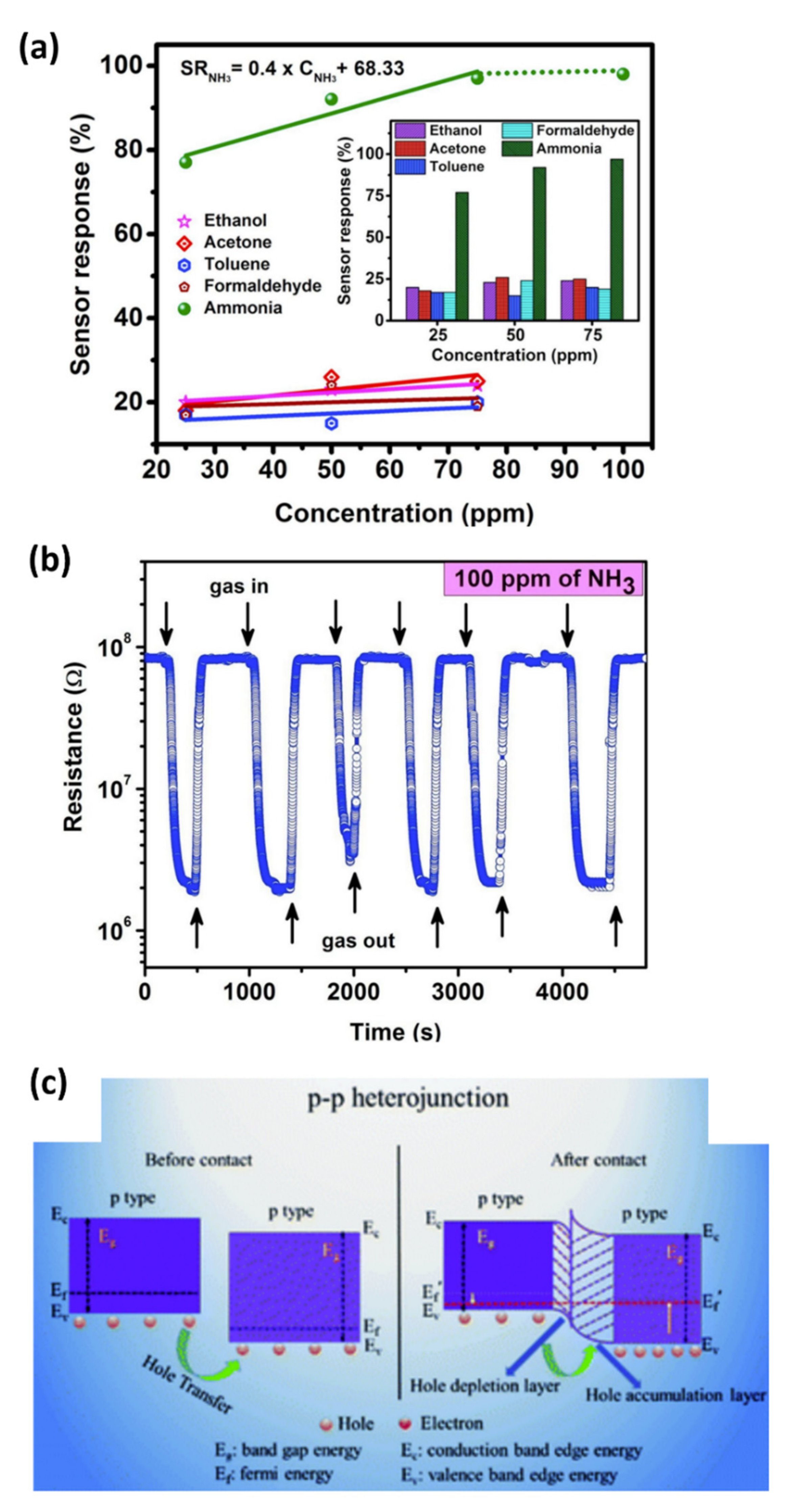
4.1.3. Ammonia (NH3)
4.2. Oxidizing Gases
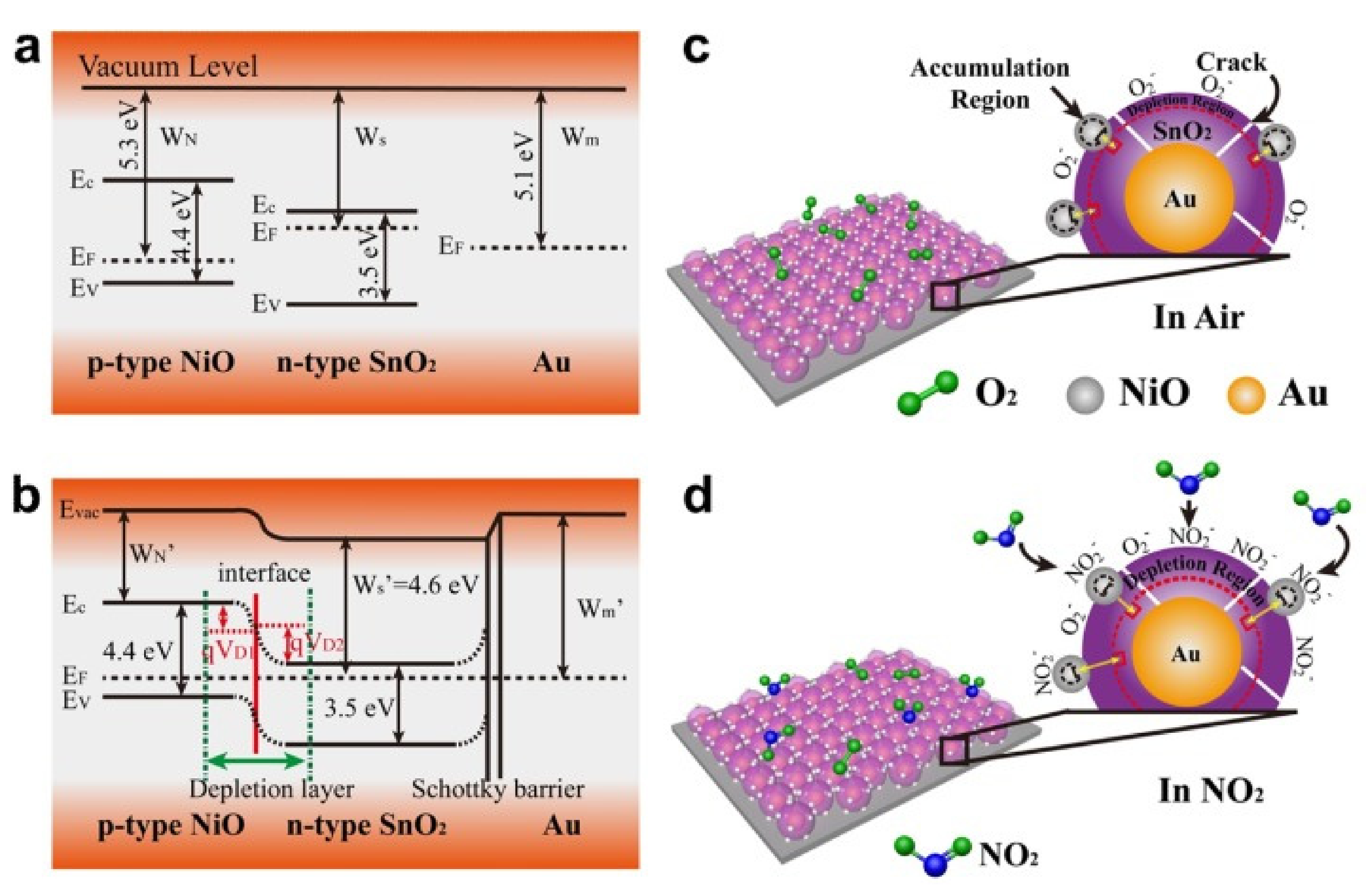
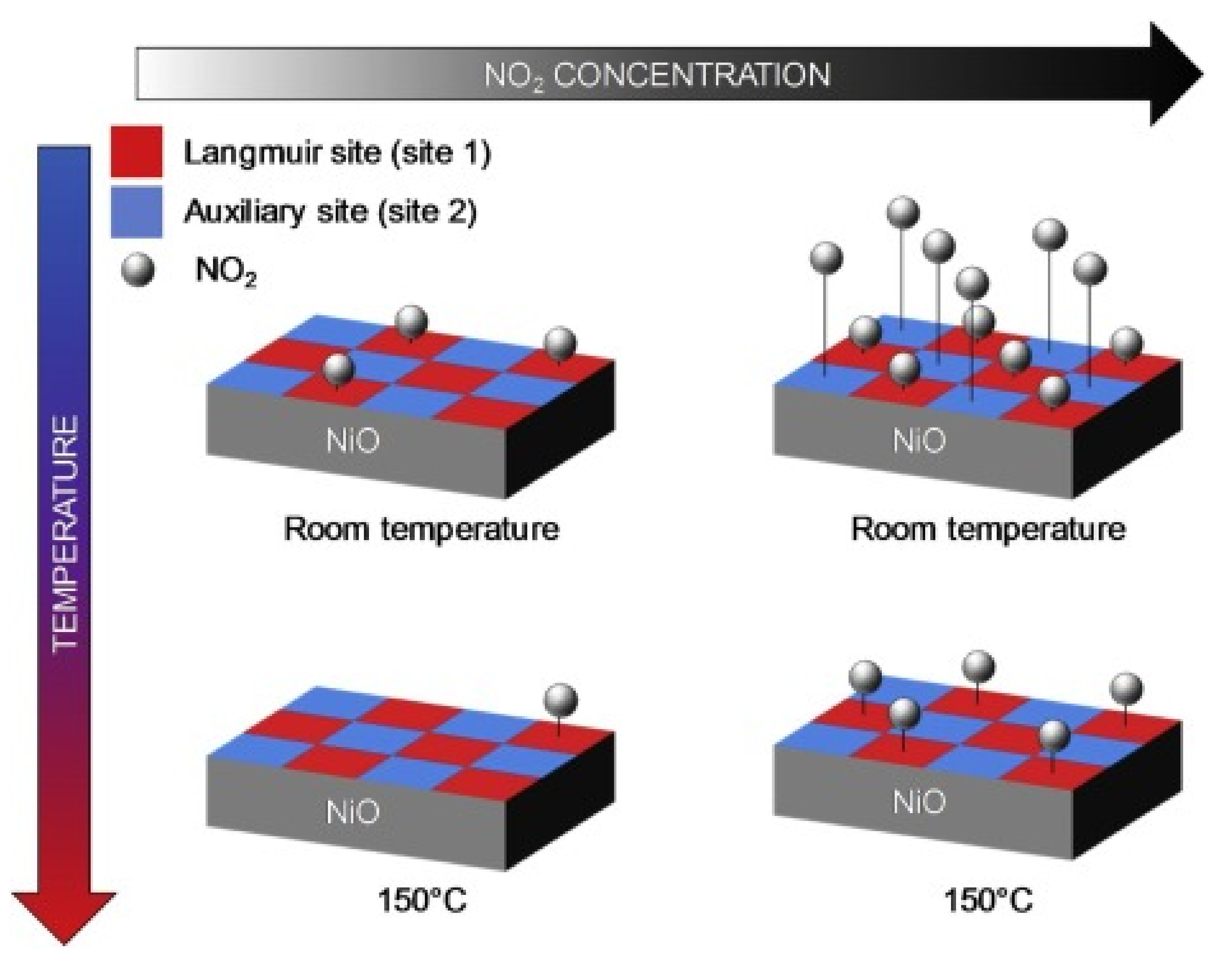
4.2.1. NO2
4.2.2. CO2
4.2.3. O3
5. Future Trends
6. Conclusions
Funding
Institutional Review Board Statement
Informed Consent Statement
Data Availability Statement
Conflicts of Interest
References
- Kishore Kumar, D.; Raghava Reddy, K.; Sadhu, V.; Shetti, N.P.; Venkata Reddy, C.; Chouhan, R.S.; Naveen, S. Metal Oxide-Based Nanosensors for Healthcare and Environmental Applications; Elsevier: Amsterdam, The Netherlands, 2020; ISBN 9780128179239. [Google Scholar]
- Shi, Y.; Xu, H.; Liu, T.; Zeb, S.; Nie, Y.; Zhao, Y.; Qin, C.; Jiang, X. Advanced development of metal oxide nanomaterials for H2 gas sensing applications. Mater. Adv. 2021, 2, 1530–1569. [Google Scholar] [CrossRef]
- Moumen, A.; Zappa, D.; Poli, N.; Comini, E. Catalyst–Assisted vapor liquid solid growth of α-Bi2O3 nanowires for acetone and ethanol detection. Sens. Actuators B Chem. 2021, 346, 130432. [Google Scholar] [CrossRef]
- Moumen, A.; Kaur, N.; Poli, N.; Zappa, D.; Comini, E. One dimensional ZnO nanostructures: Growth and chemical sensing performances. Nanomaterials 2020, 10, 1940. [Google Scholar] [CrossRef] [PubMed]
- Barsan, N.; Koziej, D.; Weimar, U. Metal oxide-based gas sensor research: How to? Sens. Actuators B Chem. 2007, 121, 18–35. [Google Scholar] [CrossRef]
- Moumen, A.; Hartiti, B.; Comini, E.; El Khalidi, Z.; Arachchige, H.M.M.M.; Fadili, S.; Thevenin, P. Preparation and characterization of nanostructured CuO thin films using spray pyrolysis technique. Superlattices Microstruct. 2019, 127, 2–10. [Google Scholar] [CrossRef]
- Fine, G.F.; Cavanagh, L.M.; Afonja, A.; Binions, R. Metal oxide semi-conductor gas sensors in environmental monitoring. Sensors 2010, 10, 5469–5502. [Google Scholar] [CrossRef] [Green Version]
- Kim, H.J.; Lee, J.H. Highly sensitive and selective gas sensors using p-type oxide semiconductors: Overview. Sens. Actuators B Chem. 2014, 192, 607–627. [Google Scholar] [CrossRef]
- Korotcenkov, G.; Brinzari, V.; Pronin, I.A.; Ham, M.H.; Cho, B.K. Metal oxides for application in conductometric gas sensors: How to choose? Solid State Phenom. 2017, 266, 187–195. [Google Scholar] [CrossRef]
- Moumen, A.; Konar, R.; Zappa, D.; Teblum, E.; Perelshtein, I.; Lavi, R.; Ruthstein, S.; Nessim, G.D.; Comini, E. Robust Room-Temperature NO2 Sensors from Exfoliated 2D Few-Layered CVD-Grown Bulk Tungsten Di-selenide (2H-WSe2). ACS Appl. Mater. Interfaces 2021, 13, 4316–4329. [Google Scholar] [CrossRef]
- Metal Oxide Sensors | Sensors for Metal Oxides | Alphasense. 2022. Available online: https://www.alphasense.com/products/metal-oxide-sensors/ (accessed on 22 December 2021).
- Abegunde, O.O.; Akinlabi, E.T.; Oladijo, O.P.; Akinlabi, S.; Ude, A.U. Overview of thin film deposition techniques. AIMS Mater. Sci. 2019, 6, 174–199. [Google Scholar] [CrossRef]
- Ji, H.; Zeng, W.; Li, Y. Gas sensing mechanisms of metal oxide semiconductors: A focus review. Nanoscale 2019, 11, 22664–22684. [Google Scholar] [CrossRef]
- Pokhrel, S.; Simion, C.E.; Quemener, V.; Bârsan, N.; Weimar, U. Investigations of conduction mechanism in Cr2O3 gas sensing thick films by ac impedance spectroscopy and work function changes measurements. Sens. Actuators B Chem. 2008, 133, 78–83. [Google Scholar] [CrossRef]
- Kumarage, G.W.C.; Comini, E. Low-Dimensional Nanostructures Based on Cobalt Oxide (Co3O4) in Chemical-Gas Sensing. Chemosensors 2021, 9, 197. [Google Scholar] [CrossRef]
- Banerjee, N.; Roy, S.; Sarkar, C.K.; Bhattacharyya, P. Effect of Humidity on Ethanol Sensing Performance of Pd Sensitized ZnO Nanorod Based Sensors. J. Surf. Interfaces Mater. 2014, 2, 154–160. [Google Scholar] [CrossRef]
- Mejía, M.I.; Restrepo, G.; Marín, J.M.; Sanjines, R.; Pulgarín, C.; Mielczarski, E.; Mielczarski, J.; Kiwi, J. Magnetron-sputtered ag surfaces. New evidence for the nature of the Ag ions intervening in bacterial inactivation. ACS Appl. Mater. Interfaces 2010, 2, 230–235. [Google Scholar] [CrossRef]
- Dolai, S.; Dey, R.; Das, S.; Hussain, S.; Bhar, R.; Pal, A.K. Cupric oxide (CuO) thin films prepared by reactive d.c. magnetron sputtering technique for photovoltaic application. J. Alloy. Compd. 2017, 724, 456–464. [Google Scholar] [CrossRef]
- Greene, J.E.; Sundgren, J.E.; Hultman, L.; Petrov, I.; Bergstrom, D.B. Development of preferred orientation in polycrystalline TiN layers grown by ultrahigh vacuum reactive magnetron sputtering. Appl. Phys. Lett. 1995, 67, 2928. [Google Scholar] [CrossRef]
- Mahendra, G.; Malathi, R.; Kedhareswara, S.P.; Lakshmi-Narayana, A.; Dhananjaya, M.; Guruprakash, N.; Hussain, O.M.; Mauger, A.; Julien, C.M. RF Sputter-Deposited Nanostructured CuO Films for Micro-Supercapacitors. Appl. Nano 2021, 2, 46–66. [Google Scholar] [CrossRef]
- Azevedo Neto, N.F.; Leite, D.M.G.; Lisboa-Filho, P.N.; da Silva, J.H.D. Role of the reactive sputtering deposition power in the phase control of cobalt oxide films. J. Vac. Sci. Technol. A 2018, 36, 061512. [Google Scholar] [CrossRef]
- Yamamoto, H.; Tanaka, S.; Hirao, K. Effects of substrate temperature on nanostructure and band structure of sputtered Co3O4 thin films. J. Appl. Phys. 2003, 93, 4158–4162. [Google Scholar] [CrossRef] [Green Version]
- Alajlani, Y.; Placido, F.; Chu, H.O.; De Bold, R.; Fleming, L.; Gibson, D. Characterisation of Cu2O/CuO thin films produced by plasma-assisted DC sputtering for solar cell application. Thin Solid Films 2017, 642, 45–50. [Google Scholar] [CrossRef] [Green Version]
- Hones, P.; Diserens, M.; Lévy, F. Characterization of sputter-deposited chromium oxide thin films. Surf. Coatings Technol. 1999, 120–121, 277–283. [Google Scholar] [CrossRef]
- Turgut, E.; Çoban, Ö.; Sarıtaş, S.; Tüzemen, S.; Yıldırım, M.; Gür, E. Oxygen partial pressure effects on the RF sputtered p-type NiO hydrogen gas sensors. Appl. Surf. Sci. 2018, 435, 880–885. [Google Scholar] [CrossRef]
- Park, S.I.; Quan, Y.J.; Kim, S.H.; Kim, H.; Kim, S.; Chun, D.M.; Lee, C.S.; Taya, M.; Chu, W.S.; Ahn, S.H. A review on fabrication processes for electrochromic devices. Int. J. Precis. Eng. Manuf. Green Technol. 2016, 3, 397–421. [Google Scholar] [CrossRef]
- Jilani, A.; Abdel-wahab, M.S.; Hammad, A.H. Advance Deposition Techniques for Thin Film and Coating. Mod. Technol. Creat. Thin Film Syst. Coat. 2017, 2, 137–149. [Google Scholar] [CrossRef] [Green Version]
- Hussain, S.; Chae, J.; Akbar, K.; Vikraman, D.; Truong, L.; Naqvi, B.A.; Abbas, Y.; Kim, H.S.; Chun, S.H.; Kim, G.; et al. Fabrication of robust hydrogen evolution reaction electrocatalyst using Ag2Se by vacuum evaporation. Nanomaterials 2019, 9, 1460. [Google Scholar] [CrossRef] [PubMed] [Green Version]
- Hamam, M.; El-Gendy, Y.; Selim, M.S.; Salem, A.M.; Teleb, N.H. Optical properties of thermally evaporated AgSbSe2 thin films. J. Appl. Sci. Res. 2009, 5, 2323–2331. [Google Scholar]
- Sahu, K.; Choudhary, S.; Khan, S.A.; Pandey, A.; Mohapatra, S. Thermal evolution of morphological, structural, optical and photocatalytic properties of CuO thin films. Nano Struct. Nano Objects 2019, 17, 92–102. [Google Scholar] [CrossRef]
- Vignesh Kumar, M.; Muthulakshmi, S.; Paulfrit, A.A.; Pandiarajan, J.; Jeyakumaran, N.; Prithivikumaran, N. Structural and Optical Behaviour of Thermally Evaporated p-Type Nickel Oxide Thin Film for Solar Cell Applications. Natl. Conf. Mater. Energy Storage Convers. 2014, 6, 5174–5177. [Google Scholar]
- Pereira, S.; Gonçalves, A.; Correia, N.; Pinto, J.; Pereira, L.; Martins, R.; Fortunato, E. Electrochromic behavior of NiO thin films deposited by e-beam evaporation at room temperature. Sol. Energy Mater. Sol. Cells 2014, 120, 109–115. [Google Scholar] [CrossRef]
- Al-Kuhaili, M.F. Characterization of copper oxide thin films deposited by the thermal evaporation of cuprous oxide (Cu2O). Vacuum 2008, 82, 623–629. [Google Scholar] [CrossRef]
- De Los Santos Valladares, L.; Salinas, D.H.; Dominguez, A.B.; Najarro, D.A.; Khondaker, S.I.; Mitrelias, T.; Barnes, C.H.W.; Aguiar, J.A.; Majima, Y. Crystallization and electrical resistivity of Cu2O and CuO obtained by thermal oxidation of Cu thin films on SiO2/Si substrates. Thin Solid Films 2012, 520, 6368–6374. [Google Scholar] [CrossRef]
- De Los Santos Valladares, L.; Ionescu, A.; Holmes, S.; Barnes, C.H.W.; Bustamante Domínguez, A.; Avalos Quispe, O.; González, J.C.; Milana, S.; Barbone, M.; Ferrari, A.C.; et al. Characterization of Ni thin films following thermal oxidation in air. J. Vac. Sci. Technol. B Nanotechnol. Microelectron. Mater. Process. Meas. Phenom. 2014, 32, 051808. [Google Scholar] [CrossRef] [Green Version]
- Djebian, R.; Boudjema, B.; Kabir, A.; Sedrati, C. Physical characterization of CuO thin films obtained by thermal oxidation of vacuum evaporated Cu. Solid State Sci. 2020, 101, 106147. [Google Scholar] [CrossRef]
- Hajakbari, F. Characterization of nanocrystalline nickel oxide thin films prepared at different thermal oxidation temperatures. J. Nanostruct. Chem. 2020, 10, 97–103. [Google Scholar] [CrossRef]
- Figueiredo, V.; Elangovan, E.; Gonçalves, G.; Barquinha, P.; Pereira, L.; Franco, N.; Alves, E.; Martins, R.; Fortunato, E. Effect of post-annealing on the properties of copper oxide thin films obtained from the oxidation of evaporated metallic copper. Appl. Surf. Sci. 2008, 254, 3949–3954. [Google Scholar] [CrossRef]
- Rakotovao, F.; Tao, Z.; Panicaud, B.; Grosseau-Poussard, J.L.; Geandier, G.; Renault, P.O.; Goudeau, P.; Boudet, N.; Blanc, N.; Vitoux, H.; et al. Strains in thermally growing Cr2O3 films measured in situ using synchrotron X-rays. Mater. Sci. Forum 2017, 905, 52–59. [Google Scholar] [CrossRef]
- Vila-Fungueiriño, J.M.; Bachelet, R.; Saint-Girons, G.; Gendry, M.; Gich, M.; Gazquez, J.; Ferain, E.; Rivadulla, F.; Rodriguez-Carvajal, J.; Mestres, N.; et al. Integration of functional complex oxide nanomaterials on silicon. Front. Phys. 2015, 3, 1–12. [Google Scholar] [CrossRef] [Green Version]
- Vaz, C.A.F.; Wang, H.Q.; Ahn, C.H.; Henrich, V.E.; Baykara, M.Z.; Schwendemann, T.C.; Pilet, N.; Albers, B.J.; Schwarz, U.D.; Zhang, L.H.; et al. Interface and electronic characterization of thin epitaxial Co3O4 films. Surf. Sci. 2009, 603, 291–297. [Google Scholar] [CrossRef] [Green Version]
- Vaz, C.A.F.; Altman, E.I.; Henrich, V.E. Exchange bias and interface electronic structure in Ni/Co3O4 (011). Phys. Rev. B Condens. Matter Mater. Phys. 2010, 81, 1–7. [Google Scholar] [CrossRef] [Green Version]
- Vaz, C.A.F.; Henrich, V.E.; Ahn, C.H.; Altman, E.I. Growth and characterization of thin epitaxial Co3O4 (111) films. J. Cryst. Growth 2009, 311, 2648–2654. [Google Scholar] [CrossRef] [Green Version]
- Kawaguchi, K.; Kita, R.; Nishiyama, M.; Morishita, T. Molecular beam epitaxy growth of CuO and Cu2O films with controlling the oxygen content by the flux ratio of Cu/O+. J. Cryst. Growth 1994, 143, 221–226. [Google Scholar] [CrossRef]
- Budde, M.; Remmele, T.; Tschammer, C.; Feldl, J.; Franz, P.; Lähnemann, J.; Cheng, Z.; Hanke, M.; Ramsteiner, M.; Albrecht, M.; et al. Plasma-assisted molecular beam epitaxy of NiO on GaN(00.1). J. Appl. Phys. 2020, 127, 015306. [Google Scholar] [CrossRef]
- Budde, M.; Tschammer, C.; Franz, P.; Feldl, J.; Ramsteiner, M.; Goldhahn, R.; Feneberg, M.; Barsan, N.; Oprea, A.; Bierwagen, O. Structural, optical, and electrical properties of unintentionally doped NiO layers grown on MgO by plasma-assisted molecular beam epitaxy. J. Appl. Phys. 2018, 123, 195301. [Google Scholar] [CrossRef]
- Liu, X.; Cao, L.; Guo, Z.; Li, Y.; Gao, W.; Zhou, L. A review of perovskite photovoltaic materials’ synthesis and applications via chemical vapor deposition method. Materials 2019, 12, 3304. [Google Scholar] [CrossRef] [PubMed] [Green Version]
- Madhuri, K.V. Thermal Protection Coatings of Metal Oxide Powders; Elsevier: Amsterdam, The Netherlands, 2020; ISBN 9780128175057. [Google Scholar]
- Nanda, A.; Singh, V.; Jha, R.K.; Sinha, J.; Avasthi, S.; Bhat, N. Growth-Temperature Dependent Unpassivated Oxygen Bonds Determine the Gas Sensing Abilities of Chemical Vapor Deposition-Grown CuO Thin Films. ACS Appl. Mater. Interfaces 2021, 13, 21936–21943. [Google Scholar] [CrossRef]
- Alarcón-Lladó, E.; Estradé, S.; Prades, J.D.; Hernandez-Ramírez, F.; Arbiol, J.; Peiró, F.; Ibáñez, J.; Artús, L.; Morante, J.R. Substrate effects on the structural and photoresponse properties of CVD grown ZnO nanostructures: Alumina vs. silica. CrystEngComm 2011, 13, 656–662. [Google Scholar] [CrossRef]
- Barreca, D.; Massignan, C.; Daolio, S.; Fabrizio, M.; Piccirillo, C.; Armelao, L.; Tondello, E. Composition and microstructure of cobalt oxide thin films obtained from a novel cobalt(II) precursor by chemical vapor deposition. Chem. Mater. 2001, 13, 588–593. [Google Scholar] [CrossRef]
- Holzschuh, H.; Suhr, H. Deposition of copper oxide (Cu2O, CuO) thin films at high temperatures by plasma-enhanced CVD. Appl. Phys. A Solids Surfaces 1990, 51, 486–490. [Google Scholar] [CrossRef]
- Sousa, P.M.; Silvestre, A.J.; Conde, O. Cr2O3 thin films grown at room temperature by low pressure laser chemical vapour deposition. Thin Solid Films 2011, 519, 3653–3657. [Google Scholar] [CrossRef] [Green Version]
- Sousa, P.M.; Silvestre, A.J.; Popovici, N.; Conde, O. Morphological and structural characterization of CrO2/Cr2O3 films grown by Laser-CVD. Appl. Surf. Sci. 2005, 247, 423–428. [Google Scholar] [CrossRef]
- Carta, B.G.; Natali, M.; Rossetto, G.; Zanella, P.; Salmaso, G.; Restello, S.; Rigato, V. A Comparative Study of Cr2O3 Thin Films Obtained by MOCVD using Three Different Precursors. Chem. Vap. Depos. 2005, 11, 375–380. [Google Scholar] [CrossRef]
- Niu, G.; Saint-Girons, G.; Vilquin, B. Epitaxial Systems Combining Oxides and Semiconductors; Elsevier Inc.: Amsterdam, The Netherlands, 2013; ISBN 9780123878397. [Google Scholar]
- Chandrakala, M.; Raj Bharath, S.; Maiyalagan, T.; Arockiasamy, S. Synthesis, crystal structure and vapour pressure studies of novel nickel complex as precursor for NiO coating by metalorganic chemical vapour deposition technique. Mater. Chem. Phys. 2017, 201, 344–353. [Google Scholar] [CrossRef]
- Basato, M.; Faggin, E.; Tubaro, C.; Veronese, A.C. Volatile square planar β-imino carbonyl enolato complexes of Pd(II) and Ni(II) as potential MOCVD precursors. Polyhedron 2009, 28, 1229–1234. [Google Scholar] [CrossRef]
- Liu, A.; Zhu, H.; Guo, Z.; Meng, Y.; Liu, G.; Fortunato, E.; Martins, R.; Shan, F. Solution Combustion Synthesis: Low-Temperature Processing for p-Type Cu:NiO Thin Films for Transparent Electronics. Adv. Mater. 2017, 29, 1701599. [Google Scholar] [CrossRef]
- Danks, A.E.; Hall, S.R.; Schnepp, Z. The evolution of “sol-gel” chemistry as a technique for materials synthesis. Mater. Horizons 2016, 3, 91–112. [Google Scholar] [CrossRef] [Green Version]
- File:SolGelTechnologyStages.svg - Wikimedia Commons. 2022. Available online: https://commons.wikimedia.org/wiki/File:SolGelTechnologyStages.svg (accessed on 22 December 2021).
- Prabhu, R.R.; Saritha, A.C.; Shijeesh, M.R.; Jayaraj, M.K. Fabrication of p-CuO/n-ZnO heterojunction diode via sol-gel spin coating technique. Mater. Sci. Eng. B Solid State Mater. Adv. Technol. 2017, 220, 82–90. [Google Scholar] [CrossRef]
- Goumri-Said, S.; Khan, W.; Boubaker, K.; Turgut, G.; Sönmez, E.; Minar, J.; Bououdina, M.; Kanoun, M.B. Europium incorporation dynamics within NiO films deposited by sol-gel spin coating: Experimental and theoretical studies. Mater. Res. Bull. 2019, 118, 110525. [Google Scholar] [CrossRef]
- Dolai, S.; Dey, R.; Hussain, S.; Bhar, R.; Pal, A.K. Synthesis, characterization and photo-response of p-type cupric oxide thin films prepared by sol-gel technique. Mater. Sci. Eng. B Solid State Mater. Adv. Technol. 2018, 236–237, 153–161. [Google Scholar] [CrossRef]
- Zhao, S.; Shen, Y.; Zhou, P.; Zhang, J.; Zhang, W.; Chen, X.; Wei, D.; Fang, P.; Shen, Y. Highly selective NO2 sensor based on p-type nanocrystalline NiO thin films prepared by sol–gel dip coating. Ceram. Int. 2018, 44, 753–759. [Google Scholar] [CrossRef]
- Chtouki, T.; El Mrabet, M.; Tarbi, A.; Goncharova, I.; Erguig, H. Comprehensive review of the morphological, linear and nonlinear optical characterization of spin-coated NiO thin films for optoelectronic applications. Opt. Mater. 2021, 118, 111294. [Google Scholar] [CrossRef]
- Ahmed, A.A.; Hashim, M.R.; Rashid, M. Control of the structural, electrical and optical properties of spin coated NiO films by varying precursor molarity. Thin Solid Films 2019, 690, 137554. [Google Scholar] [CrossRef]
- Akinkuade, S.T.; Meyer, W.E.; Nel, J.M. Effects of thermal treatment on structural, optical and electrical properties of NiO thin films. Phys. B Condens. Matter 2019, 575, 411694. [Google Scholar] [CrossRef]
- Bretos, I.; Jiménez, R.; Ricote, J.; Calzada, M.L. Low-temperature crystallization of solution-derived metal oxide thin films assisted by chemical processes. Chem. Soc. Rev. 2018, 47, 291–308. [Google Scholar] [CrossRef] [Green Version]
- Yao, C.; Hu, W.; Ismail, M.; Thatikonda, S.K.; Hao, A.; He, S.; Qin, N.; Huang, W.; Bao, D. Coexistence of resistive switching and magnetism modulation in sol-gel derived nanocrystalline spinel Co3O4 thin films. Curr. Appl. Phys. 2019, 19, 1286–1295. [Google Scholar] [CrossRef]
- Lun, T.T.; Liu, C.Q.; Wang, N.; Zhai, X.N.; Song, M.S.; Ge, Q.; Zhang, X.Y.; Liu, S.M.; Wang, H.L.; Jiang, W.W.; et al. Preparation of compact CuO films by sol-gel spin coating technique. Mater. Lett. 2019, 257, 126745. [Google Scholar] [CrossRef]
- Absike, H.; Labrim, H.; Hartiti, B.; Tahri, M.; Ez-Zahraouy, H. Influence of spinning speed on the physical properties of sol-gel spin coated CuO films. Mol. Cryst. Liq. Cryst. 2020, 711, 18–31. [Google Scholar] [CrossRef]
- Brinker, C.J.; Hurd, A.J.; Schunk, P.R.; Frye, G.C.; Ashley, C.S. Review of sol-gel thin film formation. J. Non. Cryst. Solids 1992, 147–148, 424–436. [Google Scholar] [CrossRef] [Green Version]
- Janarthanan, B.; Thirunavukkarasu, C.; Maruthamuthu, S.; Manthrammel, M.A.; Shkir, M.; Al Faify, S.; Selvakumar, M.; Reddy, V.R.M.; Park, C. Basic deposition methods of thin films. J. Mol. Struct. 2021, 1241, 130606. [Google Scholar] [CrossRef]
- Varela, A.I.G.; Aymerich, M.; García, D.N.; Martín, Y.C.; de Beule, P.A.A.; Álvarez, E.; Bao-Varela, C.; Flores-Arias, M.T. Sol-Gel Glass Coating Synthesis for Different Applications: Active Gradient-Index Materials, Microlens Arrays and Biocompatible Channels. Recent Appl. Sol Gel Synth. 2017, 5, 231–252. [Google Scholar] [CrossRef] [Green Version]
- Andrade-Sanchez, M.E.; Hernandez-Perez, M.A.; Garciá-Pacheco, G.; Ortega-Avilés, M. Temperature and pH effect on reaction mechanism and particle size of nanostructured Co3O4 thin films obtained by sol-gel/dip-coating. Mater. Res. Express 2021, 8, 025015. [Google Scholar] [CrossRef]
- Shariffudin, S.S.; Khalid, S.S.; Sahat, N.M.; Sarah, M.S.P.; Hashim, H. Preparation and Characterization of Nanostructured CuO Thin Films using Sol-gel Dip Coating. IOP Conf. Ser. Mater. Sci. Eng. 2015, 99, 012007. [Google Scholar] [CrossRef]
- Tanaya, H.; Vinoth, D.S.; Alshahrani, M.T.T.; Shkir, H.H.S.M. Tuning the Optical, Electrical, and Optoelectronic Properties of CuO Thin Films Fabricated by Facile SILAR Dip-Coating Technique for Photosensing Applications. J. Inorg. Organomet. Polym. Mater. 2021, 31, 2606–2614. [Google Scholar] [CrossRef]
- Ray, S.C. Preparation of copper oxide thin film by the sol–gel-like dip technique and study of their structural and optical properties. Sol. Energy Mater. Sol. Cells 2001, 68, 307–312. [Google Scholar] [CrossRef]
- Lon, D. 1 Scientific Concept of Nanocatalysis; Elsevier: Amsterdam, The Netherlands, 2019; ISBN 9780128157497. [Google Scholar]
- Dridi, S.; Bitri, N.; Mahjoubi, S.; Chaabouni, F.; Ly, I. One-step spray of Cu2NiSnS4 thin films as absorber materials for photovoltaic applications. J. Mater. Sci. Mater. Electron. 2020, 31, 7193–7199. [Google Scholar] [CrossRef] [Green Version]
- Gavrilovi, T.V.; Jovanovi, D.J.; Dramićanin, M.D. Synthesis of Multifunctional Inorganic Materials: From Micrometer to Nanometer Dimensions; Elsevier: Amsterdam, The Netherlands, 2018; ISBN 978-0-12-813731-4. [Google Scholar] [CrossRef]
- Shinde, S.K.; Mohite, S.M.; Kadam, A.A.; Yadav, H.M.; Ghodake, G.S.; Rajpure, K.Y.; Lee, D.S.; Kim, D. Effect of deposition parameters on spray pyrolysis synthesized CuO nanoparticle thin fi lms for higher supercapacitor performance. J. Electroanal. Chem. 2019, 850, 113433. [Google Scholar] [CrossRef]
- Gomaa, M.M.; Sayed, M.H.; Patil, V.L.; Boshta, M.; Patil, P.S. Gas sensing performance of sprayed NiO thin films toward NO2 gas. J. Alloys Compd. 2021, 885, 160908. [Google Scholar] [CrossRef]
- Louardi, A.; Rmili, A.; Chtouki, T.; Elidrissi, B.; Erguig, H.; Bachiri, A. El Effect of annealing treatment on Co3O4 thin films properties prepared by spray pyrolysis. J. Mater. Environ. Sci. 2017, 8, 485–493. [Google Scholar]
- Arca, E.; Fleischer, K.; Krasnikov, S.A.; Shvets, I. Effect of Chemical Precursors on the Optical and Electrical Properties of p-Type Transparent Conducting Cr2O3:(Mg, N). J. Phys. Chem. C 2013, 117, 21901–21907. [Google Scholar] [CrossRef] [Green Version]
- Glynn, C.; Dwyer, C.O. Solution Processable Metal Oxide Thin Film Deposition and Material Growth for Electronic and Photonic Devices. Adv. Mater. Interfaces 2017, 4, 1600610. [Google Scholar] [CrossRef]
- Daira, R.; Kabir, A.; Boudjema, B.; Sedrati, C. Structural and optical transmittance analysis of CuO thin films deposited by the spray pyrolysis method. Solid State Sci. 2020, 104, 106254. [Google Scholar] [CrossRef]
- Abdulkarem, S.; Mohammed, M.; Tariq, Z.; Mohammed, I.; Saeed, M. The influence of deposition temperatures on the structural and optical properties for NiO nanostructured thin films prepared via spray pyrolysis technique. Chem. Data Collect. 2021, 33, 100677. [Google Scholar] [CrossRef]
- Oh, S.W.; Bang, H.J.; Bae, Y.C.; Sun, Y. Effect of calcination temperature on morphology, crystallinity and electrochemical properties of nano-crystalline metal oxides (Co3O4, CuO, and NiO) prepared via ultrasonic spray pyrolysis. J. Power Sources 2007, 173, 502–509. [Google Scholar] [CrossRef]
- Kee, S.; Kim, W.; Jung, J.; Choi, M. Effect of Via Pitch on the Extrusion Behavior of Cu-filled TSV. Korean J. Met. Mater. 2018, 56, 449–458. [Google Scholar] [CrossRef] [Green Version]
- Mallik, A.; Ray, B.C. Evolution of Principle and Practice of Electrodeposited Thin Film : A Review on Effect of Temperature and Sonication. Int. J. Electrochem. 2011, 2011, 1–16. [Google Scholar] [CrossRef] [Green Version]
- Firat, Y.E. Materials Science in Semiconductor Processing Influence of current density on Al : NiO thin films via electrochemical deposition : Semiconducting and electrochromic properties. Mater. Sci. Semicond. Process. 2020, 109, 104958. [Google Scholar] [CrossRef]
- Wu, M.; Huang, Y.; Jow, J.; Yang, W.; Hsieh, C.; Tsai, H. Anodically potentiostatic deposition of flaky nickel oxide nanostructures and their electrochemical performances. Int. J. Hydrog. Energy 2008, 33, 2921–2926. [Google Scholar] [CrossRef]
- Ghalmi, Y.; Habelhames, F.; Sayah, A.; Bahloul, A.; Nessark, B.; Shalabi, M.; Nunzi, J.M. Capacitance performance of NiO thin films synthesized by direct and pulse potentiostatic methods. Ionics 2019, 25, 6025–6033. [Google Scholar] [CrossRef]
- Eyraud, A.B.M.; Hornebecq, F.V.V.; Knauth, T.D.P. Single-step electrodeposition of superhydrophobic black NiO thin films. J. Appl. Electrochem. 2019, 49, 621–629. [Google Scholar] [CrossRef]
- Dalavi, D.S.; Suryavanshi, M.J. Efficient maximization of coloration by modification in morphology of electrodeposited NiO thin films prepared with different surfactants. J. Solid State Electrochem. 2012, 16, 253–263. [Google Scholar] [CrossRef]
- Cruz-Ortiz, B.R.; Garcia-Lobato, M.A.; Larios-Durán, E.R.; Múzquiz-Ramos, E.M.; Ballesteros-Pacheco, J.C. Potentiostatic electrodeposition of nanostructured NiO thin films for their application as electrocatalyst. J. Electroanal. Chem. 2016, 772, 38–45. [Google Scholar] [CrossRef]
- Saadeddin, I.; Suleiman, M.; Salman, H.; Zrikem, K.; Song, G.; Rougier, A. Optimization of low value electrodeposition parameters of nano-structured NiO electrochromic thin films. Solid State Ionics 2019, 343, 115129. [Google Scholar] [CrossRef]
- Kafi, F.S.B.; Jayathileka, K.M.D.C.; Wijesundera, R.P.; Siripala, W. Effect of Bath pH on Interfacial Properties of Electrodeposited n-Cu2O Films. Phys. Status Solidi 2018, 255, 1700541. [Google Scholar] [CrossRef]
- Wijesundera, R.P.; Hidaka, M.; Koga, K.; Sakai, M.; Siripala, W.; Choi, J. Effects of annealing on the properties and structure of electrodeposited semiconducting Cu–O thin films. Phys. Status Solidi 2007, 244, 4629–4642. [Google Scholar] [CrossRef]
- You, A.; Be, M.A.Y.; In, I. Comparative analysis of electrodeposited cobalt oxide thin films by chronoamperometry and chronopotentiometry modes for supercapacitor application. Comparative Analysis of Electrodeposited Cobalt oxide Thin Films by Chronoamperometry and Chronopotentiome. AIP Conf. Proc. 2020, 2265, 030615. [Google Scholar]
- Kim, G.H.; Park, Y.S.; Yang, J.; Jang, M.J.; Jeong, J.; Lee, J.; Park, H.; Park, Y.H.; Choi, S.M.; Lee, J. Effects of Annealing Temperature on the Oxygen Evolution Reaction Activity of Copper–Cobalt Oxide Nanosheets. Nanomaterials 2021, 11, 657. [Google Scholar] [CrossRef] [PubMed]
- Hassan, H.B.; Hamid, Z.A. Electrodeposited Ni e Cr2O3 nanocomposite anodes for ethanol electrooxidation. Int. J. Hydrogen Energy 2011, 36, 5117–5127. [Google Scholar] [CrossRef]
- Jiao, D.; Liu, W.; Xue, L.; Zhou, Q.; Yan, Y. A Dense Cr2O3/Al2O3 Composite Ceramic Coating Prepared by Electrodeposition and Sealing with Al2O3. Coatings 2019, 9, 14. [Google Scholar] [CrossRef] [Green Version]
- Ni, J.Q.; Robarge, W.P.; Xiao, C.; Heber, A.J. Volatile organic compounds at swine facilities: A critical review. Chemosphere 2012, 89, 769–788. [Google Scholar] [CrossRef] [PubMed]
- Galstyan, V.; D’Arco, A.; Di Fabrizio, M.; Poli, N.; Lupi, S.; Comini, E. Detection of volatile organic compounds: From chemical gas sensors to terahertz spectroscopy. Rev. Anal. Chem. 2021, 40, 33–57. [Google Scholar] [CrossRef]
- Amiri, V.; Roshan, H.; Mirzaei, A.; Neri, G.; Ayesh, A.I. Nanostructured metal oxide-based acetone gas sensors: A review. Sensors 2020, 20, 3096. [Google Scholar] [CrossRef]
- Hotovy, I.; Rehacek, V.; Kemeny, M.; Ondrejka, P.; Kostic, I.; Mikolasek, M.; Spiess, L. Preparation and gas-sensing properties of very thin sputtered NiO films. J. Electr. Eng. 2021, 72, 61–65. [Google Scholar] [CrossRef]
- Ayyala, S.K.; Covington, J.A. Nickel-oxide based thick-film gas sensors for volatile organic compound detection. Chemosensors 2021, 9, 247. [Google Scholar] [CrossRef]
- Predanocy, M.; Hotovy, I.; Caplovicova, M.; Rehacek, V.; Kosc, I.; Spiess, L. Sputtered NiO thin films for organic vapours testing. In Proceedings of the The Ninth International Conference on Advanced Semiconductor Devices and Mircosystems, Smolenice, Slovakia, 11–15 November 2012; Institute of Electrical and Electronics Engineers (IEEE): Piscataway, NJ, USA; pp. 291–294. [Google Scholar] [CrossRef]
- Bhowmick, T.; Nag, S.; Majumder, S.B. Understanding the ethanol and acetone sensing behaviour of CuO thin films through elements of gas diffusion theory. Mater. Chem. Phys. 2021, 262, 124286. [Google Scholar] [CrossRef]
- Srinivasan, P.; Srinivasan, P.; Kulandaisamy, A.; Mani, G.; Babu, K.; Tsuchiya, K.; Rayappan, J. Development of an acetone sensor using nanostructured Co3O4 thin films for exhaled breath analysis. RSC Adv. 2019, 9, 30226–30239. [Google Scholar] [CrossRef] [Green Version]
- Ghosh, A.; Maity, A.; Banerjee, R.; Majumder, S.B. Volatile organic compound sensing using copper oxide thin films: Addressing the cross sensitivity issue. J. Alloys Compd. 2017, 692, 108–118. [Google Scholar] [CrossRef]
- Szkudlarek, A.; Kollbek, K.; Klejna, S.; Rydosz, A. Electronic sensitization of CuO thin films by Cr-doping for enhanced gas sensor response at low detection limit. Mater. Res. Express 2018, 5, 126406. [Google Scholar] [CrossRef]
- Rydosz, A. The use of copper oxide thin films in gas-sensing applications. Coatings 2018, 8, 425. [Google Scholar] [CrossRef] [Green Version]
- Said, A.A. The role of copper-chromium oxide catalysts in the thermal decomposition of ammonium perchlorate. J. Therm. Anal. 1991, 37, 959–967. [Google Scholar] [CrossRef]
- Gagaoudakis, E.; Michail, G.; Katerinopoulou, D.; Moschovis, K.; Iliopoulos, E.; Kiriakidis, G.; Binas, V.; Aperathitis, E. Transparent p-type NiO:Al thin films as room temperature hydrogen and methane gas sensors. Mater. Sci. Semicond. Process. 2020, 109, 104922. [Google Scholar] [CrossRef]
- Shang, Y.; Shi, W.; Zhao, R.; Ahmed, M.M.; Li, J.; Du, J. Simple self-assembly of 3D laminated CuO/SnO2 hybrid for the detection of triethylamine. Chinese Chem. Lett. 2020, 31, 2055–2058. [Google Scholar] [CrossRef]
- Dyndal, K.; Zarzycki, A.; Andrysiewicz, W.; Grochala, D.; Marszalek, K.; Rydosz, A. Cuo-ga2o3 thin films as a gas-sensitive material for acetone detection. Sensors 2020, 20, 3142. [Google Scholar] [CrossRef] [PubMed]
- Han, N.; Pan, G.; Zheng, J.; Wang, R.; Wang, Y. Co3O4-ZnO p-n heterostructure nanomaterials film and its enhanced photoelectric response to visible lights at near room temperature. Mater. Res. 2019, 22, 1–11. [Google Scholar] [CrossRef]
- Kavitha, G.; Arul, K.T.; Babu, P. Enhanced acetone gas sensing behavior of n-ZnO/p-NiO nanostructures. J. Mater. Sci. Mater. Electron. 2018, 29, 6666–6671. [Google Scholar] [CrossRef]
- Yang, F.; Wang, F.; Guo, Z. Characteristics of binary WO3@CuO and ternary WO3@PDA@CuO based on impressive sensing acetone odor. J. Colloid Interface Sci. 2018, 524, 32–41. [Google Scholar] [CrossRef]
- Park, S.; An, S.; Ko, H.; Lee, C. Enhanced ethanol sensing properties of TeO2 nanorods functionalized with Co3O4 nanoparticles. J. Nanosci. Nanotechnol. 2015, 15, 439–444. [Google Scholar] [CrossRef]
- Mirzaei, A.; Park, S.; Sun, G.J.; Kheel, H.; Lee, C.; Lee, S. Fe2O3/Co3O4 composite nanoparticle ethanol sensor. J. Korean Phys. Soc. 2016, 69, 373–380. [Google Scholar] [CrossRef] [Green Version]
- Doan, T.L.H.; Kim, J.Y.; Lee, J.H.; Nguyen, L.H.T.; Dang, Y.T.; Bui, K.B.T.; Pham, A.T.T.; Mirzaei, A.; Phan, T.B.; Kim, S.S. Preparation of n-ZnO/p-Co3O4 heterojunctions from zeolitic imidazolate frameworks (ZIF-8/ZIF-67) for sensing low ethanol concentrations. Sensors Actuators B Chem. 2021, 348, 130684. [Google Scholar] [CrossRef]
- Tong, W.; Wang, Y.; Bian, Y.; Wang, A.; Han, N.; Chen, Y. Sensitive Cross-Linked SnO2:NiO Networks for MEMS Compatible Ethanol Gas Sensors. Nanoscale Res. Lett. 2020, 15, 1–12. [Google Scholar] [CrossRef]
- Yang, B.; Liu, J.; Qin, H.; Liu, Q.; Jing, X.; Zhang, H.; Li, R.; Huang, G.; Wang, J. PtO2-nanoparticles functionalized CuO polyhedrons for n-butanol gas sensor application. Ceram. Int. 2018, 44, 10426–10432. [Google Scholar] [CrossRef]
- Hoppe, M.; Ababii, N.; Postica, V.; Lupan, O.; Polonskyi, O.; Schütt, F.; Kaps, S.; Sukhodub, L.F.; Sontea, V.; Strunskus, T.; et al. (CuO-Cu2O)/ZnO:Al heterojunctions for volatile organic compound detection. Sens. Actuators B Chem. 2018, 255, 1362–1375. [Google Scholar] [CrossRef]
- Fang, J.; Zhu, Y.; Wu, D.; Zhang, C.; Xu, S.; Xiong, D.; Yang, P.; Wang, L.; Chu, P.K. Gas sensing properties of NiO/SnO2 heterojunction thin film. Sens. Actuators B Chem. 2017, 252, 1163–1168. [Google Scholar] [CrossRef]
- Kumar, A.; Sanger, A.; Kumar, A.; Chandra, R. Highly sensitive and selective CO gas sensor based on a hydrophobic SnO2/CuO bilayer. RSC Adv. 2016, 6, 47178–47184. [Google Scholar] [CrossRef]
- Chen, H.I.; Hsiao, C.Y.; Chen, W.C.; Chang, C.H.; Liu, I.P.; Chou, T.C.; Liu, W.C. Formaldehyde sensing characteristics of a nio-based sensor decorated with Pd nanoparticles and a Pd Thin film. IEEE Trans. Electron Devices 2018, 65, 1956–1961. [Google Scholar] [CrossRef]
- Crowl, D.A.; Jo, Y. Do The hazards and risks of hydrogen. J. Loss Prev. Process Ind. 2007, 20, 158–164. [Google Scholar] [CrossRef]
- Chou, P.C.; Chen, H.I.; Liu, I.P.; Chen, C.C.; Liou, J.K.; Hsu, K.S.; Liu, W.C. Hydrogen sensing performance of a nickel oxide (NiO) thin film-based device. Int. J. Hydrogen Energy 2015, 40, 729–734. [Google Scholar] [CrossRef]
- Guziewicz, M.; Klata, P.; Grochowski, J.; Golaszewska, K.; Kaminska, E.; Domagala, J.Z.; Witkowski, B.A.; Kandyla, M.; Chatzimanolis, C.; Kompitsas, M.; et al. Hydrogen sensing properties of thin NiO films deposited by RF sputtering. Procedia Eng. 2012, 47, 746–749. [Google Scholar] [CrossRef] [Green Version]
- El khalidi, Z.; Hartiti, B.; Fadili, S.; Thevenin, P. Nickel oxide optimization using Taguchi design for hydrogen detection. Int. J. Hydrogen Energy 2018, 43, 12574–12583. [Google Scholar] [CrossRef]
- Almaev, A.V.; Kushnarev, B.O.; Chernikov, E.V.; Novikov, V.A.; Korusenko, P.M.; Nesov, S.N. Structural, electrical and gas-sensitive properties of Cr2O3 thin films. Superlattices Microstruct. 2021, 151, 106835. [Google Scholar] [CrossRef]
- Abubakar, D.; Ahmed, N.M.; Mahmud, S.; Algadri, N.A. Properties of NiO nanostructured growth using thermal dry oxidation of nickel metal thin film for hydrogen gas sensing at room temperature. Mater. Res. Express 2017, 4, 075009. [Google Scholar] [CrossRef]
- Park, S.; Sun, G.J.; Kheel, H.; Hyun, S.K.; Jin, C.; Lee, C. Hydrogen gas sensing of Co3O4-Decorated WO3 nanowires. Met. Mater. Int. 2016, 22, 156–162. [Google Scholar] [CrossRef]
- Huo, L.; Yang, X.; Liu, Z.; Tian, X.; Qi, T.; Wang, X.; Yu, K.; Sun, J.; Fan, M. Modulation of potential barrier heights in Co3O4/SnO2 heterojunctions for highly H2-selective sensors. Sens. Actuators B Chem. 2017, 244, 694–700. [Google Scholar] [CrossRef]
- Rydosz, A.; Maziarz, W.; Brudnik, A.; Czapla, A.; Zakrzewska, K. CuO and CuO/TiO2-y thin-film gas sensors of H2 and NO2. In Proceedings of the 2018 XV International Scientific Conference on Optoelectronic and Electronic Sensors (COE), Warsaw, Poland, 17–20 June 2018; pp. 2016–2019. [Google Scholar]
- Lupan, O.; Ababii, N.; Mishra, A.K.; Bodduluri, M.T.; Magariu, N.; Vahl, A.; Krüger, H.; Wagner, B.; Faupel, F.; Adelung, R.; et al. Heterostructure-based devices with enhanced humidity stability for H2 gas sensing applications in breath tests and portable batteries. Sens. Actuators A Phys. 2021, 329, 112804. [Google Scholar] [CrossRef]
- Kosc, I.; Hotovy, I.; Rehacek, V.; Griesseler, R.; Predanocy, M.; Wilke, M.; Spiess, L. Sputtered TiO2 thin films with NiO additives for hydrogen detection. Appl. Surf. Sci. 2013, 269, 110–115. [Google Scholar] [CrossRef]
- Biswas, B.; Dey, A.; Roy, S.; Ray, S.; Sarkar, S.K. Pd Doped TiO2-CuO Mixed Metal Oxide Thin Film Sensor for H2 Sensing Application. In Proceedings of the Pd Doped TiO2-CuO Mixed Metal Oxide Thin Film Sensor for H2 Sensing Application, Kalyani, India, 23–24 March 2019; pp. 202–205. [Google Scholar] [CrossRef]
- Kandyla, M.; Chatzimanolis-Moustakas, C.; Koumoulos, E.P.; Charitidis, C.; Kompitsas, M. Nanocomposite NiO:Au hydrogen sensors with high sensitivity and low operating temperature. Mater. Res. Bull. 2014, 49, 552–559. [Google Scholar] [CrossRef] [Green Version]
- Sta, I.; Jlassi, M.; Kandyla, M.; Hajji, M.; Koralli, P.; Krout, F.; Kompitsas, M.; Ezzaouia, H. Surface functionalization of sol-gel grown NiO thin films with palladium nanoparticles for hydrogen sensing. Int. J. Hydrogen Energy 2016, 41, 3291–3298. [Google Scholar] [CrossRef]
- Kandyla, M.; Chatzimanolis-Moustakas, C.; Guziewicz, M.; Kompitsas, M. Nanocomposite NiO:Pd hydrogen sensors with sub-ppm detection limit and low operating temperature. Mater. Lett. 2014, 119, 51–55. [Google Scholar] [CrossRef] [Green Version]
- Yadav, P.; Kumar, A.; Sanger, A.; Gautam, Y.K.; Singh, B.P. Sputter-Grown Pd-Capped CuO Thin Films for a Highly Sensitive and Selective Hydrogen Gas Sensor. J. Electron. Mater. 2021, 50, 192–200. [Google Scholar] [CrossRef]
- Hoa, N.D.; An, S.Y.; Dung, N.Q.; Van Quy, N.; Kim, D. Synthesis of p-type semiconducting cupric oxide thin films and their application to hydrogen detection. Sens. Actuators B Chem. 2010, 146, 239–244. [Google Scholar] [CrossRef]
- Cynthia, S.R.; Sivakumar, R.; Sanjeeviraja, C.; Gopalakrishnan, C.; Jeyadheepan, K. Room temperature ammonia gas sensing characteristics of copper oxide-tin oxide composite thin films prepared by radio frequency magnetron sputtering technique. J. Mater. Sci. Mater. Electron. 2020, 31, 18018–18036. [Google Scholar] [CrossRef]
- Cynthia, S.R.; Sivakumar, R.; Sanjeeviraja, C. Ternary CuO:SnO2:ZnO (1:1:1) composite thin film for room temperature gas sensor application. Optik 2021, 234, 166615. [Google Scholar] [CrossRef]
- Sharma, S.; Kumar, A.; Singh, N.; Kaur, D. Excellent room temperature ammonia gas sensing properties of n-MoS2/p-CuO heterojunction nanoworms. Sens. Actuators B Chem. 2018, 275, 499–507. [Google Scholar] [CrossRef]
- Yue, Q.; Shao, Z.; Chang, S.; Jingbo, L. Adsorption of gas molecules on monolayer MoS2. Nanoscale Res. Lett. 2014, 8, 1–7. [Google Scholar]
- Ponmudi, S.; Sivakumar, R.; Sanjeeviraja, C.; Gopalakrishnan, C.; Jeyadheepan, K. Tuning the Morphology of Cr2O3:CuO (50:50) Thin Films by RF Magnetron Sputtering for Room Temperature Sensing Application; Elsevier B.V.: Amsterdam, The Netherlands, 2019; Volume 466, ISBN 9145652252. [Google Scholar]
- Li, Z.; Li, H.; Wu, Z.; Wang, M.; Luo, J.; Torun, H.; Hu, P.; Yang, C.; Grundmann, M.; Liu, X.; et al. Advances in designs and mechanisms of semiconducting metal oxide nanostructures for high-precision gas sensors operated at room temperature. Mater. Horiz. 2019, 6, 470–506. [Google Scholar] [CrossRef] [Green Version]
- Barth, P.J.; Muller, B.; Wagner, U.; Bittinger, A. Quantitative analysis of parenchymal and vascular alterations in NO2-induced lung injury in rats. Eur. Respir. J. 1995, 8, 1115–1121. [Google Scholar] [CrossRef] [Green Version]
- Wu, Y.; Hu, M.; Tian, Y. Room temperature NO2-sensing properties of hexagonal tungsten oxide nanorods. Chin. Phys. B 2017, 26, 20701. [Google Scholar] [CrossRef]
- Zhang, B.; Cheng, M.; Liu, G.; Gao, Y.; Zhao, L.; Li, S.; Wang, Y.; Liu, F.; Liang, X.; Zhang, T.; et al. Room Temperature NO2 Gas Sensor Based on Porous Co3O4 Slices/Reduced Graphene Oxide Hybrid; Elsevier B.V.: Amsterdam, The Netherlands, 2018; Volume 263, ISBN 8643185167. [Google Scholar]
- Hsueh, T.J.; Wu, S.S. Highly sensitive Co3O4 nanoparticles/MEMS NO2 gas sensor with the adsorption of the Au nanoparticles. Sens. Actuators B Chem. 2021, 329, 129201. [Google Scholar] [CrossRef]
- Khot, S.; Phalake, S.; Mahadik, S.; Baragale, M.; Jagadale, S.; Burungale, V.; Navale, Y.; Patil, V.; Patil, V.; Patil, P.; et al. Synthesis of cuo thin film sensors by spray pyrolysis method for NO2 gas detection. Mater. Today Proc. 2020, 43, 2694–2697. [Google Scholar] [CrossRef]
- Al-Jumaili, B.E.; Rzaij, J.M.; Ibraheam, A. Nanoparticles of CuO thin films for room temperature NO2 gas detection: Annealing time effect. Mater. Today Proc. 2021, 42, 2603–2608. [Google Scholar] [CrossRef]
- Kampitakis, V.; Gagaoudakis, E.; Zappa, D.; Comini, E.; Aperathitis, E.; Kostopoulos, A.; Kiriakidis, G.; Binas, V. Highly sensitive and selective NO2 chemical sensors based on Al doped NiO thin films. Mater. Sci. Semicond. Process. 2020, 115, 105149. [Google Scholar] [CrossRef]
- Urso, M.; Leonardi, S.G.; Neri, G.; Petralia, S.; Conoci, S.; Priolo, F.; Mirabella, S. Room temperature detection and modelling of sub-ppm NO2 by low-cost nanoporous NiO film. Sens. Actuators B Chem. 2020, 305, 127481. [Google Scholar] [CrossRef]
- Benedict, S.; Singh, M.; Naik, T.R.R.; Shivashankar, S.A.; Bhat, N. Microwave-Synthesized NiO as a Highly Sensitive and Selective Room-Temperature NO2 Sensor. ECS J. Solid State Sci. Technol. 2018, 7, Q3143–Q3147. [Google Scholar] [CrossRef] [Green Version]
- Drozdowska, K.; Welearegay, T.; Österlund, L.; Smulko, J. Combined chemoresistive and in situ FTIR spectroscopy study of nanoporous NiO films for light-activated nitrogen dioxide and acetone gas sensing. Sens. Actuators B Chem. 2022, 353. [Google Scholar] [CrossRef]
- Chizhov, A.; Rumyantseva, M.; Gaskov, A. Light Activation of Nanocrystalline Metal Oxides for Gas Sensing: Principles, Achievements, Challenges. Nanomaterials 2021, 11, 892. [Google Scholar] [CrossRef] [PubMed]
- Gu, D.; Li, X.; Wang, H.; Li, M.; Xi, Y.; Chen, Y.; Wang, J.; Rumyntseva, M.N.; Gaskov, A.M. Light enhanced VOCs sensing of WS2 microflakes based chemiresistive sensors powered by triboelectronic nangenerators. Sens. Actuators B Chem. 2018, 256, 992–1000. [Google Scholar] [CrossRef]
- Patil, V.L.; Vanalakar, S.A.; Patil, P.S.; Kim, J.H. Fabrication of nanostructured ZnO thin films based NO2 gas sensor via SILAR technique. Sens. Actuators B Chem. 2017, 239, 1185–1193. [Google Scholar] [CrossRef]
- Nalage, S.R.; Chougule, M.A.; Sen, S.; Patil, V.B. Novel method for fabrication of NiO sensor for NO2 monitoring. J. Mater. Sci. Mater. Electron. 2013, 24, 368–375. [Google Scholar] [CrossRef]
- Rahmani, M.B.; Keshmiri, S.H.; Shafiei, M.; Latham, K.; Wlodarski, W.; Plessis, J.D.; Kalantar-Zadeh, K. Transition from n- to p-type of spray pyrolysis deposited Cu doped ZnO thin films for NO2 sensing. Sens. Lett. 2009, 7, 621–628. [Google Scholar] [CrossRef]
- Li, Y.; Wlodarski, W.; Galatsis, K.; Moslih, S.H.; Cole, J.; Russo, S.; Rockelmann, N. Gas sensing properties of p-type semiconducting Cr-doped TiO2 thin films. Sens. Actuators B Chem. 2002, 83, 160–163. [Google Scholar] [CrossRef]
- Miller, D.R.; Akbar, S.A.; Morris, P.A. Nanoscale metal oxide-based heterojunctions for gas sensing: A review. Sens. Actuators B Chem. 2014, 204, 250–272. [Google Scholar] [CrossRef]
- Wang, Y.; Liu, C.; Wang, Z.; Song, Z.; Zhou, X.; Han, N.; Chen, Y. Sputtered SnO2:NiO Thin Films on Self-Assembled Au Nanoparticle Arrays for MEMS Compatible NO2 Gas Sensors; Elsevier B.V.: Amsterdam, The Netherlands, 2019; Volume 278, ISBN 8610625583. [Google Scholar]
- Li, T.T.; Bao, N.; Geng, A.F.; Yu, H.; Yang, Y.; Dong, X.T. Study on room temperature gas-sensing performance of cuo film-decorated ordered porous zno composite by In2O3 sensitization. R. Soc. Open Sci. 2018, 5, 171788. [Google Scholar] [CrossRef] [Green Version]
- Wimmer-Teubenbacher, R.; Sosada-Ludwikowska, F.; Travieso, B.Z.; Defregger, S.; Tokmak, O.; Niehaus, J.S.; Deluca, M.; Köck, A. CuO thin films functionalized with gold nanoparticles for conductometric carbon dioxide gas sensing. Chemosensors 2018, 6, 56. [Google Scholar] [CrossRef] [Green Version]
- Ishihara, T.; Kometani, K.; Hashida, M.; Takita, Y. Application of Mixed Oxide Capacitor to the Selective Carbon Dioxide Sensor: I. Measurement of Carbon Dioxide Sensing Characteristics. J. Electrochem. Soc. 1991, 138, 173–176. [Google Scholar] [CrossRef]
- Chapelle, A.; El Younsi, I.; Vitale, S.; Thimont, Y.; Nelis, T.; Presmanes, L.; Barnabé, A.; Tailhades, P. Improved semiconducting CuO/CuFe2O4 nanostructured thin films for CO2 gas sensing. Sens. Actuators B Chem. 2014, 204, 407–413. [Google Scholar] [CrossRef] [Green Version]
- Joshi, G.; Rajput, J.K.; Purohit, L.P. SnO2–Co3O4 pores composites for CO2 gas sensing at low operating temperature. Microporous Mesoporous Mater. 2021, 326, 2–9. [Google Scholar] [CrossRef]
- Tanvir, N.B.; Yurchenko, O.; Laubender, E.; Pohle, R.; Sicard, O.V.; Urban, G. Zinc peroxide combustion promoter in preparation of CuO layers for conductometric CO2 sensing. Sens. Actuators B Chem. 2018, 257, 1027–1034. [Google Scholar] [CrossRef]
- Srinivasan, P.; Ezhilan, M.; Kulandaisamy, A.J.; Babu, K.J.; Rayappan, J.B.B. Room temperature chemiresistive gas sensors: Challenges and strategies—A mini review. J. Mater. Sci. Mater. Electron. 2019, 30, 15825–15847. [Google Scholar] [CrossRef]
- Bejaoui, A.; Guerin, J.; Zapien, J.A.; Aguir, K. Theoretical and experimental study of the response of CuO gas sensor under ozone. Sens. Actuators B Chem. 2014, 190, 8–15. [Google Scholar] [CrossRef]
- Kumar, R.; Baratto, C.; Faglia, G.; Sberveglieri, G.; Bontempi, E.; Borgese, L. Tailoring the textured surface of porous nanostructured NiO thin films for the detection of pollutant gases. Thin Solid Films 2015, 583, 233–238. [Google Scholar] [CrossRef]
- Paralikis, A.; Gagaoudakis, E.; Kampitakis, V.; Aperathitis, E.; Kiriakidis, G.; Binas, V. Study on the ozone gas sensing properties of rf-sputtered Al-doped NiO films. Appl. Sci. 2021, 11, 3104. [Google Scholar] [CrossRef]


| Material | Synthesis Method | Operating Temperature (°C) | Gas/ppm | Response | Response/Recovery Time (s) | LOD | Long-Term Stability/Reproducibility | Ref. |
|---|---|---|---|---|---|---|---|---|
| NiO | Photolithography-assisted spin coating | 350 | Ethanol/5 ppm | 1.27 a | 80 s/120 s | NA | NA/NA | [110] |
| NiO | Magnetron sputtering | 300 | Ethanol/5 ppm | 5 b | 167 s/99 s | 0.1 ppm | NA/NA | [111] |
| CuO | Wet chemical method | 300 | Acetone/50 ppm | 2 b | NA/NA | NA | 180 days/3 cycles | [112] |
| Co3O4 | Spray pyrolysis | RT | Acetone/50 ppm | 235 a | 6 s/4 s | 1 ppm | 60 days/5 cycles | [113] |
| Al-doped NiO | Magnetron sputtering | RT+UV irradiation | Methane/NA | 58% b | 1373 s/249 s | NA | NA/3 cycles | [118] |
| CuO-Ga2O3 | Magnetron sputtering | 300 | Acetone/1.25 ppm | 1.35 a | 187 s/525 s | NA | NA/NA | [120] |
| n-ZnO/p-NiO | Wet-chemical-route-assisted spin coating | 300 | Acetone/500 ppm | NA | 13 s/18 s | NA | NA/NA | [122] |
| PtO2-functionalized CuO | Two-step method | 180 | n-butanol/100 ppm | 12 a | 2.4 s/9.2 s | NA | 30 days/6 cycles | [128] |
| NiO/SnO2 | Magnetron sputtering | 250 | Ethanol/100 ppm | 7.9 NA | 15 s/100 s | 100 ppb | NA/4 cycles | [130] |
| NiO | Magnetron sputtering | 250 | H2/1% | 416 b | 7 s/153 s | ≤50 ppm | NA/NA | [134] |
| NiO | Spray pyrolysis | 300 | H2/500 ppm | 55 b | 38 s/41 s | NA | NA/NA | [136] |
| Cr2O3 | Magnetron sputtering | 400 | H2/2000 ppm | 40%NA | NA | NA | NA/NA | [137] |
| Co3O4/SnO2 | Soak-calcination method | 300 | H2/50 ppm | 30% b | NA | NA | NA/24 cycles | [140] |
| Al2O3/CuO | ALD | 350 | H2/100 ppm | 80% b | 20.8 s/59.9 s | NA | 70 days/3 cycles | [142] |
| Au-functionalized NiO | Magnetron sputtering | 125 | H2/500 ppm | 1 b | 15 min to ∼5 min/NA | 2 ppm | NA/NA | [145] |
| NiO | Magnetron sputtering | 140 | H2/10000 ppm | 14 b | 3 min/NA | NA | NA/NA | [141] |
| Pd-functionalized CuO | Magnetron sputtering | 300 | H2/1000 ppm | 3 a | 10 s/50 s | NA | 21 days/NA | [148] |
| CuO/SnO2 | Magnetron sputtering | RT | NH3/100 ppm | 3353 a | 266 s/35 s | NA | 6 months/5 cycles | [150] |
| CuO/SnO2/ZnO | Magnetron sputtering | RT | NH3/100 ppm | 2057 a | 294 s/47 s | NA | 6 months/5 cycles | [151] |
| MoS2/CuO | Magnetron sputtering | RT | NH3/100 ppm | 47% b | 17 s/26 s | NA | 70 days/15 cycles | [152] |
| Cr2O3/CuO | Magnetron sputtering | RT | NH3/25 ppm | 77% b | 11 s/14 s | 14.1 ppm | NA/6 cycles | [154] |
| CuO | Spray pyrolysis | 200 | NO2/ 5 ppm | 56.23% b | 20.57 s/235.2 s | NA | N/A | [160] |
| NiO | Sol–gel spin coating | 200 | NO2/ 20 ppm | 57.3% b | 20 s/498 s | NA | 20 days/ | [169] |
| Al/NiO | RF sputtering | 200 | NO2/ 1 ppm | 576 b | 2160 s/3300 s | NA | 365 days | [162] |
| 2.4% rGO-Co3O4 | Facile two-step method | RT | NO2/ 5 ppm | 26.8% b | 210 s/60 s | 50 ppb | 20 days/5 cycles | [158] |
| Au-functionalized CuO | Electron-beam lithography, thermal evaporation | 300 | CO2/2000 ppm | 365% b | 258 s/264 s | N/A | 14 days/NA | [175] |
| CuO/CuFe2O4 | RF sputtering | 250 | CO2/5000 ppm | 40 b | 3300 s/480 s | NA/NA | NA/NA | [177] |
| SnO2–Co3O4 | Sol–gel spin coating | 30 | CO2/2000 ppm | 13.68 b | 2 s/12 s | NA | NA/NA | [178] |
| NiO | Chemical-bath deposition | RT | NO2/ 140 ppb | 3.5 b | 75 s/174 s | 20 ppb | 30 days/NA/NA | [163] |
| NiO | Microwave-assisted deposition | RT | NO2/ 3 ppm | 4991% b | 30 s/45 s | 200 ppb | NA/NA | [164] |
| NiO | Sol–gel spin coating | 200 | NO2/ 200 ppm | 23.3 b | 20 s/498 s | NA | 30 days/NA | [169] |
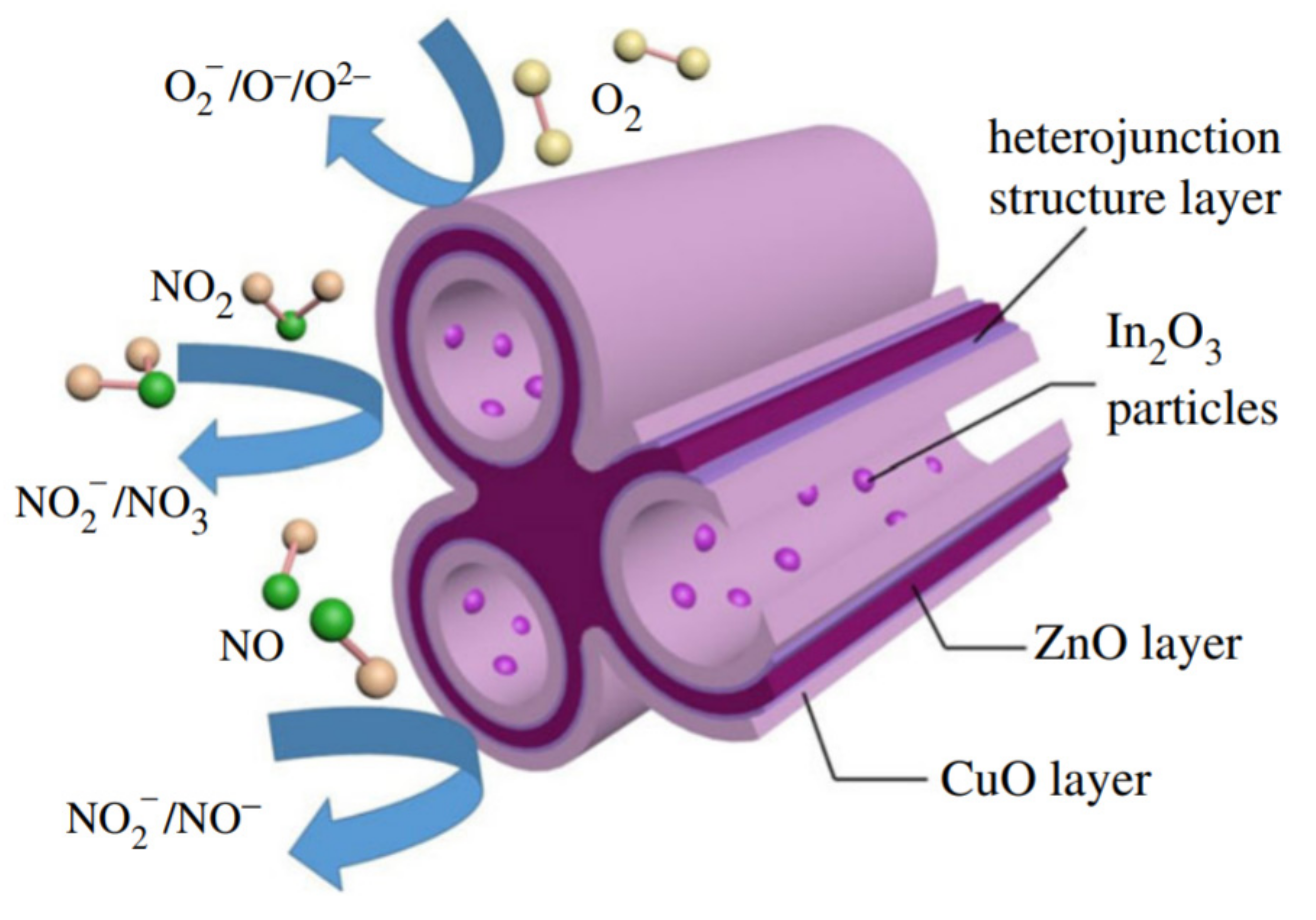
| In2O3–CuO/ZnO | Electroplating and chemical plating | RT | NOx/ 100 ppm | 82 b | 7 s/NA | 1000 ppb | 6 months/NA | [174] |
| Al-doped NiO | RF sputtering | 150 | O3/80 ppb | 5.17% b | 189.6 s/243.6 s | 10 ppb | NA/NA | [183] |
Publisher’s Note: MDPI stays neutral with regard to jurisdictional claims in published maps and institutional affiliations. |
© 2022 by the authors. Licensee MDPI, Basel, Switzerland. This article is an open access article distributed under the terms and conditions of the Creative Commons Attribution (CC BY) license (https://creativecommons.org/licenses/by/4.0/).
Share and Cite
Moumen, A.; Kumarage, G.C.W.; Comini, E. P-Type Metal Oxide Semiconductor Thin Films: Synthesis and Chemical Sensor Applications. Sensors 2022, 22, 1359. https://doi.org/10.3390/s22041359
Moumen A, Kumarage GCW, Comini E. P-Type Metal Oxide Semiconductor Thin Films: Synthesis and Chemical Sensor Applications. Sensors. 2022; 22(4):1359. https://doi.org/10.3390/s22041359
Chicago/Turabian StyleMoumen, Abderrahim, Gayan C. W. Kumarage, and Elisabetta Comini. 2022. "P-Type Metal Oxide Semiconductor Thin Films: Synthesis and Chemical Sensor Applications" Sensors 22, no. 4: 1359. https://doi.org/10.3390/s22041359
APA StyleMoumen, A., Kumarage, G. C. W., & Comini, E. (2022). P-Type Metal Oxide Semiconductor Thin Films: Synthesis and Chemical Sensor Applications. Sensors, 22(4), 1359. https://doi.org/10.3390/s22041359