Article

A Fast-Transient-Response NMOS LDO with Wide Load-Capacitance Range for Cross-Point Memory

1
School of Microelectronics, University of Science and Technology of China, Hefei 230026, China
2
State Key Laboratory of Functional Materials for Informatics, Shanghai Institute of Micro-System and Information Technology, Chinese Academy of Sciences, Shanghai 200050, China
*
Author to whom correspondence should be addressed.
Sensors 2022, 22(23), 9367; https://doi.org/10.3390/s22239367
Submission received: 15 November 2022 / Revised: 28 November 2022 / Accepted: 29 November 2022 / Published: 1 December 2022
(This article belongs to the Special Issue Advanced CMOS Integrated Circuit Design and Application II)

Abstract

:
In this paper, a fast-transient-response NMOS low-dropout regulator (LDO) with a wide load-capacitance range was presented to provide a V/2 read bias for cross-point memory. To utilize the large dropout voltage in the V/2 bias scheme, a fast loop consisting of NMOS and flipped voltage amplifier (FVA) topology was adopted with a fast transient response. This design is suitable to provide a V/2 read bias with 3.3 V input voltage and 1.65 V output voltage for different cross-point memories. The FVA-based LDO designed in the 110 nm CMOS process remained stable under a wide range of load capacitances from 0 to 10 nF and equivalent series resistance (ESR) conditions. At the capacitor-less condition, it exhibited a unity-gain bandwidth (UGB) of approximately 400 MHz at full load. For load current changes from 0 to 10 mA within an edge time of 10 ps, the simulated undershoot and settling time were only 144 mV and 50 ns, respectively. The regulator consumed 70 µA quiescent current and achieved a remarkable figure-of-merit (FOM) of 1.01 mV. At the ESR condition of a 1 µF off-chip capacitor, the simulated quiescent current, on-chip capacitor consumption, and current efficiency at full load were 8.5 µA, 2 pF, and 99.992%, respectively. The undershoot voltage was 20 mV with 800 ns settling time for a load step from 0 to 100 mA within the 10 ps edge time.

1. Introduction

With the commercialization of Intel’s Optane SSD [1], cross-point memory has attracted great interest for its high density, high capacity, and low latency. In the one-selector-one-resistor (1S1R) configuration, the memory density can reach the smallest cell size of 4 F2 (F is the feature size of a technology node) [2]. However, a critical challenge for 1S1R arrays is the large number of sneak paths that reduce the reliability and performance of the system [3]. To address this issue, on the one hand, Ovonic threshold switching (OTS) devices have shown immense potential with their low-temperature process, ultra-low off current, large drive current density, high selectivity (the ratio of on current and off current), and fast operating speed [4]. On the other hand, V/2, V/3, and other bias schemes are proposed to avoid unintentional read and write operations in cross-point arrays [5,6,7,8]. The typical V/2 bias scheme for the read operation is shown in Figure 1. V/2 bias is applied on all the word lines (WLs) and bit lines (BLs) in the standby phase. When the read-enable pulse occurs, the selected BL and selected WL turn to V and the ground, respectively. Meanwhile, the load current of the V/2 bias is transiently changed from no load to heavy load. Therefore, a reliable V/2 bias with a fast transient response is essential for the read operation.
In the V/2 bias scheme, the load current is limited since the sneak path current only exists in half-selected memory cells. In addition, advanced OTS devices with high selectivity can significantly limit the off current [9,10]. The parasitic capacitance of the selector and memory cell is dependent on the material. Moreover, the load capacitance of 1S1R memories is directly related to the size of arrays. As a result, the V/2 read bias needs to remain stable over a wide range of load capacitances.
Compared with the switching converter, a low-dropout regulator (LDO) is more suitable to drive the V/2 bias due to its low noise, small area, and fast transient response. Although novel bias schemes have been proposed for cross-point memory, few circuit-level designs have been presented. To achieve a fast transient response, flipped voltage follower (FVF) topology has been adopted in advanced LDOs [11,12]. A large on-chip output capacitor was adopted to push the output pole to a lower frequency and became the dominant pole. The fully integrated LDOs achieved good transient responses that could respond to less than 10 ns load-transient edges but occupied a large area. A trip-loop LDO based on FVF topology was proposed with only a 0.65 ns response time and 43 mV undershoot when the load changed from 0 to 10 mA within 200 ps [11]. It required an on-chip capacitor of 140 pF, consuming a large chip area. In addition, the power supply rejection (PSR) was only −20 dB at low frequencies. Some LDO systems have been proposed to supply the fast operating bias for nonvolatile memories [13,14]. However, the large on-chip capacitor was not suitable for the cross-point memory with high storage density. An internal dominant pole was designed in a LDO that significantly reduced the chip area [15], but this LDO suffered from instability at zero current load condition and could only maintain system stability within a small range of load capacitance from 0 to 25 pF. Its PSR degraded to −5 dB while reaching 1 MHz. An LDO without an output capacitor and with a direct voltage-spike detection circuit was presented with little overhead [16]. However, the edge time of load switching was 1 µs, which is too long for advanced memory. Recently, NMOS-based LDOs were proposed for low output impedance, better transient responses, and other benefits [17,18,19,20]. To drive the power transistor for low-dropout voltage, charge pumps or extra batteries must be introduced. A charge pump circuit powering the error amplifier would introduce switching noise and consume extra current and area overhead. In the cross-point memory, a read voltage (Vread) can be set between the threshold voltage of the memory cell in the RESET state (VtR) and the SET state (VtS). The V/2 bias scheme results in an inevitable voltage difference, so there is no need to minimize the dropout voltage between the input and output voltages during the read operation. For the conventional V/2 bias scheme, the read operation voltages in previous designs ranged from approximately 2.5 V to 4 V [21,22,23]. Therefore, the dropout voltage is high enough to drive the NMOS regulation FET [24]. In summary, exists is a research gap for a fully integrated LDO with a fast transient response and high area efficiency or a non-fully-integrated LDO with high performance to provide a V/2 bias for different sizes of memory arrays.
In this article, a fast-transient-response NMOS LDO based on FVA topology was proposed. The fast FVA loop provides a wide unity-gain bandwidth (UGB), which leads to a short settling time. Meanwhile, the regulator can maintain stability within a wide range of output capacitors from 0 to 10 nF and ESR conditions. This design is suitable to provide V/2 read bias for different sizes of 1S1R arrays.
The rest of this paper is organized as follows. Section 2 describes considerations of the LDO architecture. Section 3 explains the details of the proposed circuit. Section 4 shows the simulation results and a comprehensive comparison. Section 5 concludes the paper.

2. LDO Architectural Considerations

2.1. NMOS Regulation FET

NMOS utilized in LDOs leads to various benefits. First, compared with a PMOS regulation FET, the gate capacitance (CG) of the NMOS FET is smaller. Less capacitance helps push the internal poles to higher frequencies. Second, the gate-to-source voltage of the NMOS FET changes directly when the load current varies, leading to a better transient response. Moreover, the source follower structure has a low output impedance so that the output pole can also be pushed to higher frequencies, resulting in a wider loop bandwidth and faster slew rate (SR) when the load changes [19]. Finally, NMOS has a much higher electron mobility, so the NMOS-based LDO shows more area efficiency than the PMOS-based LDO. For a single-supply system, charge pumps are essential in NMOS-based LDO regulators to provide low dropout voltage. Accordingly, NMOS-based LDOs are not commonly used as PMOS-based LDOs due to the introduction of charge pumps that worsen chip area and power consumption. However, the deterioration caused by the charge pump does not exist in this design. V/2 bias scheme provides enough dropout voltage for the NMOS regulation FET to drive the load current at full load condition. In summary, an LDO adopting NMOS can benefit from the small parasitic capacitance, better transient response, low output impedance, wider loop bandwidth, faster slew rate (SR), and increased area efficiency without the cost of a charge pump, which is specific for cross-point memory applications.

2.2. Flipped Voltage Amplifier

The FVF topology is widely used in on-chip LDOs for fast transient response due to low output impedance, better regulation, and frequency compensation [25]. Two typical FVF-based LDOs are shown in Figure 2 with single-transistor control and inserted buffer. The single transistor control topology is the simplest architecture in FVF-based LDOs that can remain stable under a variety of output capacitors, with a potentially fast transient response and low voltage characteristics. The circuit is mainly composed of VSET generation, a flipped voltage follower, and a load module. VSET is controlled to be equal to VREF by a simple amplifier. Additionally, assume I1 = kI2 and (W/L)F1 = k(W/L)F2, where k is the multiplier of transistors so that the output voltage (VOUT) can be set the same as VSET. To improve the stability of the topology and enhance the transient response, a buffer can be introduced to help push the internal poles to high frequencies and set the output pole to be dominant [26].
Figure 3 shows the architecture of the flipped voltage amplifier-based LDO. First, an NMOS FET is adopted without charge pumps for a lower output impedance and higher unity-gain bandwidth. The DC bias of MF1 and MF2 are the same as those of the FVF-based LDO. The super source follower is replaced by a high-bandwidth inverting amplifier to form a fast negative feedback loop and ensure system stability. In this design, the output capacitor can be a small on-chip capacitor to improve the transient response. The pole at the gate of the NMOS transistor (pgate) being dominant in the fully integrated FVA-based LDO could provide a stable voltage regulation under a wide range of load capacitance due to the low output impedance. Furthermore, using a large off-chip ESR to push the output pole (pout) to be the dominant pole, the UGB would be improved compared with FVF-based LDO due to the low output impedance and small parasitic gate capacitance of the NMOS transistor (Cgate). In summary, the FVA-based LDO can remain stable under a wide range of output-capacitor and ESR conditions.

2.3. Poles and Stability Considerations

FVF-based LDOs achieve a good transient response within a short edge time compared with traditional resistor-based LDO regulators. However, the stability of the system is dependent on a large on-chip capacitor or ESR capacitance. To avoid significant consumption of area, the dominant pole is designed at the gate of the NMOS within a wide range of load capacitances in the proposed FVA topology. Moreover, the FVA-based LDO adopting the output pole as the dominant pole exhibits superior performance at ESR conditions. The LDO structure and its poles are sketched in Figure 4 under different conditions. Due to the small CG and low output impedance of the NMOS FET, two poles pout and pgate are pushed to high frequencies, as depicted in Figure 4a. Without frequency compensation, the system may face stability problems since pout is close to pgate at the light load condition. To improve the phase margin at light or no load conditions, small series resistance–capacitance (R-C) compensation was adopted at the gate of the power transistor. This helps to push the pgate to a lower frequency and generate a left-half-plane (LHP) zero zgate. As shown in Figure 4a, pgate, pout, and zgate can be given by:
p gate = 1 [ C C + C gdp + C gsp g mbp / ( g mbp + g mp ) ] R I , C
p out = 1 C out { [ 1 / ( 1 / g mp + g mbp ) ] / / ( 1 / g mf ) / / R L }
z gate = 1 C C R C
where gmp, gmbp, and Cgsp and Cgdp are the transconductance, body-effect transconductance, and gate-to-source and gate-to-drain capacitances of MP, respectively; gmf is the transconductance of MF; CC, RC, RL, RI, and Cout are the compensation capacitor and resistance, load impedance, input resistance of the inverting amplifier, and output capacitor, respectively; and RI,C is the sum of RI and RC. To maintain the stability of the fast loop of LDO, zgate is introduced to compensate for the nondominant pole at light load. Since pout is proportional to the load impedance, it depends on 1/(gmbp + gmf) at heavy load conditions. Thus, this nondominant pole is shifted to high frequencies as the load current increases, resulting in a large UGB. Moreover, another nondominant pole pin may become nonnegligible due to the wide bandwidth. An on-chip capacitor is added at the output terminal with a small resistance to avoid the effect of the pin and enhance the transient response. As the load capacitance increases, the phase margin of the system will gradually deteriorate. Nevertheless, this regulator remains stable with a large output load capacitance.
Figure 4b shows the FVA-based LDO with an off-chip capacitor Coff. In this case, pout was designed as the dominant pole due to the large output capacitor. An LHP zero zESR was generated by ESR, which can be expressed as:
z ESR = 1 C off R ESR
At the light load condition, the dominant pole pout is placed at very low frequencies, and the stability is easily satisfied. At heavy and full load conditions, pout is shifted to high frequencies as the output resistance decreases, and the nondominant pole pgate is lower than the UGB. The LHP zero is utilized to counteract the phase shift of the pgate. Therefore, loop stability is guaranteed without R-C compensation.
In summary, the FVA-based LDO can maintain stability within a wide range of load capacitance and ESR capacitors. Compared with the FVF-based LDO, at the on-chip output capacitor condition, less capacitor is utilized in the FVA-based LDO for high area efficiency. The UGB of the fast loop is not deteriorated at heavy loads due to the ultra-low output impedance. At ESR conditions, the UGB is significantly improved owing to the lower output impedance and smaller parasitic capacitance. Owing to a wide UGB and direct feedback to the gate-to-source voltage of the NMOS FET, FVA-based LDOs would achieve a fast transient response. In addition, compared with fully integrated LDOs that adopt an internal dominant pole, the FVA-based LDO could remain stable within a wide range of load capacitances and exhibit a better transient response.

3. Proposed FVA Low-Dropout Regulator

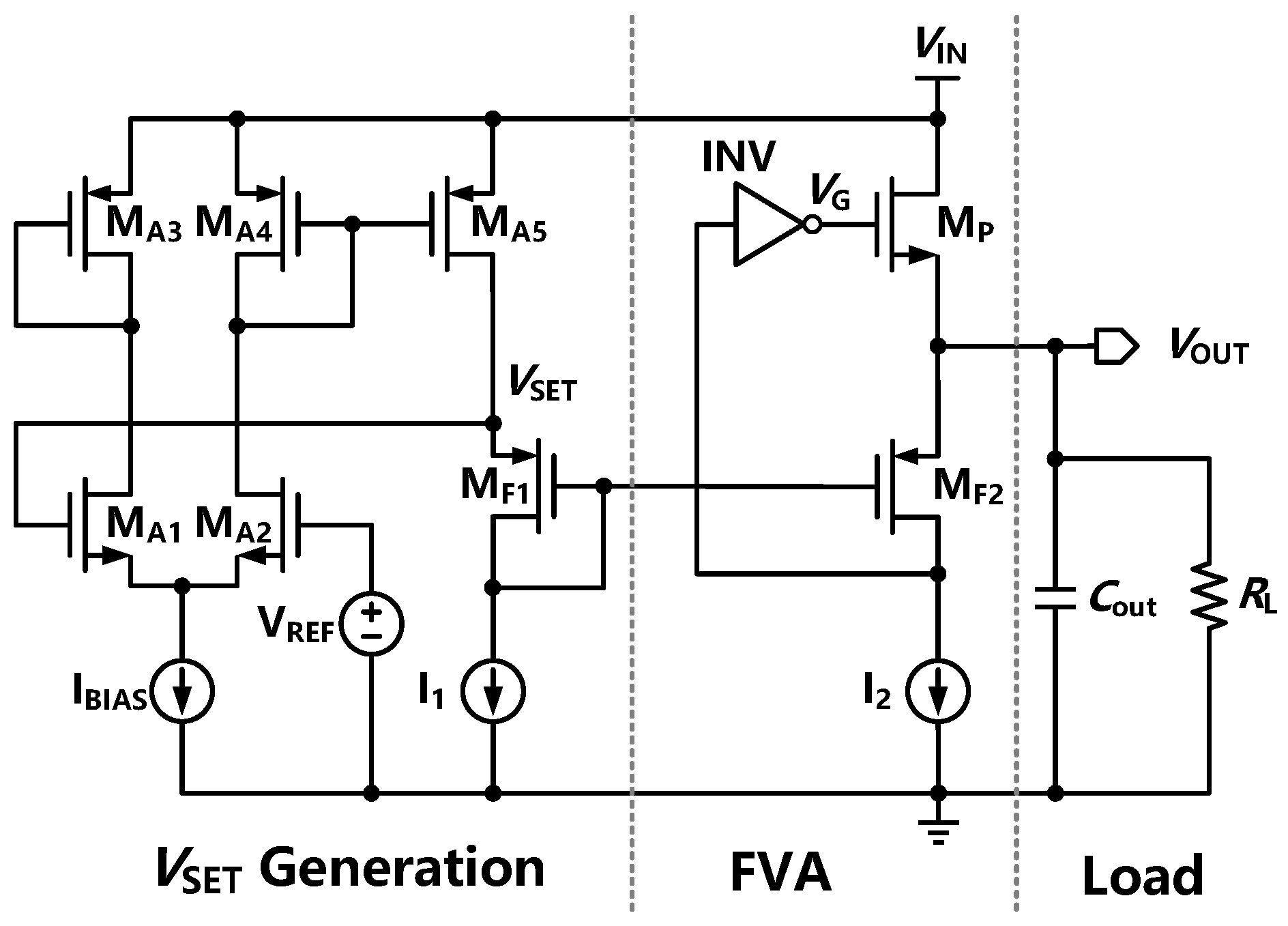
Figure 5 shows the transistor level schematic of the proposed flipped voltage amplifier-based LDO. This circuit can be divided into four parts: main LDO, output capacitor, conventional bias, and adaptive bias. Two loops are adopted in the system, including a slow loop to generate the VOUT and a fast loop to achieve better dynamics accuracy while load changes. For the slow loop, the VSET is generated by a simple error amplifier or a simple LDO circuit that could drive µA-level current. The W/L ratio of transistors M1 and M2 was set to 1:4, which is the same rate as the bias current generated by the cascode current mirror consisting of M3, M4, M10, and M11. Thus, the source-to-gate voltage of M1 (VSG1) is equal to the source-to-gate voltage of M2 (VSG2). Furthermore, VOUT is given by:
V OUT = V SET V SG 1 + V SG 2 = V SET
Therefore, VOUT can be adjusted according to the setting of VSET. The slow loop consisting of the above M1, M2, and VSET generation circuit could easily satisfy the stability. It provides accurate DC operating points for the circuit and ensures that VOUT is equal to VSET.
Similar to the FVF-based LDO, there is another fast loop to provide fast transient responses when the load current varies. To guarantee the stability of the negative feedback loop, the buffer of the FVF structure is replaced by an inverting amplifier with a wide bandwidth in the FVA topology. The fast loop consists of M2, M6, MP, and current bias. As a result, the NMOS-based LDO has more area efficiency, smaller output resistance, and smaller CG. The load regulation is less affected by different load currents or capacitances because the power transistor works as a source follower. Moreover, the FVA loop with a high UGB could provide fast transient responses within a short edge time.
The mechanism for the fast loop to respond to current transients is expressed as follows. When the load current changes from light load to heavy load, VOUT is lower than the preset voltage, and the drain voltage of M2 drops since the decrease of VSG2. The gate voltage of M9 drops and the gate voltage of MP increases due to the inverting amplifier. Consequently, the output voltage is forced to increase. In addition, the power transistor can directly provide negative feedback while voltage drops. Meanwhile, when the load current changes from heavy load to light load, VOUT is higher than the preset voltage, and the drain voltage of M2 increases as VSG2 grows. The gate voltage of M9 grows, and the gate voltage of MP is reduced as well. As a result, the output voltage is forced to decrease.
Conventional bias circuits are proposed to provide a reliable current bias for the main LDO module. The conventional bias consists of a simple current mirror and a voltage-spike detection circuit. Additionally, the voltage-spike detection circuit is added at the gate of M5 and the output terminal. The purpose of introducing the voltage-spike detection circuit is to improve the limited SR and transient response without an extra quiescent current. The output voltage is kept constant under a stable load current provided by the conventional bias circuit. When the load current varies, VOUT changes and leads to a voltage spike (ΔV) rapidly. Therefore, the current is momentarily changed, resulting in an extra dynamic current (ΔI) generation. The total and dynamic current can be expressed as follows:
I + Δ I = 1 2 μ p C ox W L ( V SG 5 V THP + Δ V ) 2
Δ I μ p C ox W L ( V SG 5 V THP + Δ V 2 ) Δ V
where μn, Cox, W/L, and VTHP are the mobility of electrons, gate oxide capacitance per unit of area, aspect ratio, and threshold voltage of a PMOS device, respectively. Moreover, C1 and R1 will introduce a pole-zero doublet at the frequency of 1/R1C1, which needs to be set lower than the minimum bandwidth of LDO at different load conditions. The high-pass characteristic of this circuit could increase the low-frequency gain of the fast FVA loop.
Without an off-chip capacitor, the internal pole pgate at the gate of the power transistor is designed as the dominant pole in the proposed FVA topology. Meanwhile, pout is designed as a nondominant pole due to the super-low output impedance at heavy load. As the load current decreases, the output impedance is increased, and pout moves to a lower frequency. Therefore, it is necessary to satisfy stability requirements at light and zero load conditions. The dominant pole pgate is high due to the lower CG and pout getting closer to the pgate, which leads to insufficient phase margin. To satisfy the stability of the fast FVA loop, R-C compensation is added to introduce an LHP zero zgate. This zero is designed as lower than pout to ensure both UGB extension and loop stability. In addition, the increase in load capacitance would result in lower frequencies of pout. Nevertheless, the system could remain stable under a wide range of load capacitances due to the small output impedance and R-C compensation. To deal with a faster transient response, the UGB of the FVA loop is designed to be wide. Meanwhile, an on-chip output capacitor is adopted to guarantee a fast transient response and filter out noise from the supply. Additionally, a small resistance is connected to the output capacitor for counteracting the phase shift of the pin.
When a large external capacitor is adopted in FVA-based LDO, pout is pushed to a low frequency and becomes the dominant pole. The ESR zero zESR could counteract the phase shift of the pgate, and R-C compensation is not required to be adopted. Since a large current would lead to a small output impedance and push pout to higher frequencies, an adaptive bias is proposed to improve the stability load regulation within a large load current. Figure 6 expresses the function of the adaptive bias module consisting of current mirrors MDB2 and MDB4. The input current obtained from the sensing load current shows a high accuracy. At a heavy load, adaptive bias is used to improve stability and load regulation. At light load, MDB3 works in the deep subthreshold region, and the adaptive bias circuit consumes ultra-low quiescent current. The generated adaptive current is added to the inverting amplifier for better stability of the FVA loop. In general, the transient response can be effectively enhanced by introducing an off-chip capacitor. This design exhibits a wider UGB and better transient response characteristics than FVF-based LDOs with off-chip capacitors. Meanwhile, it could achieve superior PSR and higher current efficiency. In fact, the introduction of large external capacitors will realize an improved transient response and lower power while sacrificing chip integration.

4. Simulation Results

The proposed design was implemented in a standard 110 nm CMOS process. At the no off-chip capacitor condition, the FVA-based LDO delivered a maximum load current of 10 mA with a 3.3 V output voltage and 1.65 V output voltage to provide V/2 read bias for cross-point memory. Additionally, the quiescent current was 70 µA. Figure 7 shows the Bode plots of the FVA loops at both zero and full load conditions (ILOAD = 0 µA and 10 mA) with zero load capacitance (CL = 0 pF). From the simulation, the zgate introduced by R-C compensation could counteract the phase shift of the pout at both conditions. To address another internal pole pin at the heavy condition, a small resistance connected to the output capacitor was adopted to generate an LHP zero at high frequencies. As expected, the phase margins of the FVA loop were 91° and 109° under 0 µA and 10 mA loads, respectively. The UGB of the system reached approximately 400 MHz at full load, leading to fast transient responses. In addition, the pole-zero doublet introduced by the voltage-spike detection circuit in low-middle frequency increases the low-frequency gain. The stability of the system does not deteriorate. To verify the stability of the system under variable load capacitance, Figure 8 presents the phase margin of the proposed LDO with a range of CL from 0 pF to 10 nF. The simulation results indicated that the phase margin was larger than 50° at both zero and full load conditions. Therefore, for a wide range of CL, the proposed LDO is stable at light and heavy load current conditions.
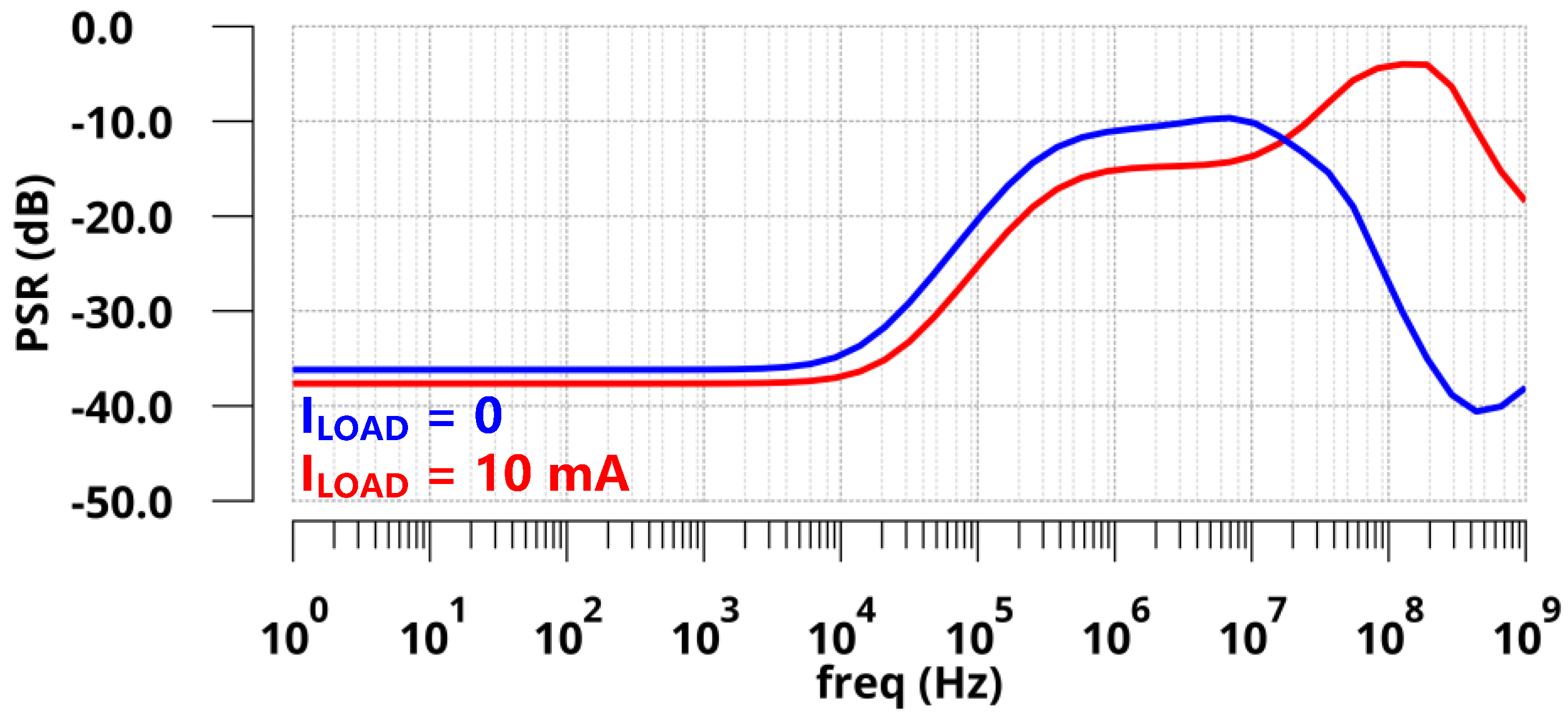
The simulated PSRs of the regulator at zero and full load conditions are presented in Figure 9. With zero CL, the simulated PSR of the proposed LDO was −17.8 dB at 1 GHz under a 10 mA load and −37.4 dB at 1 GHz under zero load. Figure 10 shows the simulated transient response of VOUT with a full current step (ILOAD changed from 0 µA to 10 mA) within an edge time of 10 ps. As shown in Figure 10a, the undershoot voltage and settling time were only 144 mV and 50 ns without CL due to the fast FVA loop. Additionally, the overshoot voltage and settling time were 121 mV and 400 ns, respectively. As shown in Figure 10b, the simulated undershoot and overshoot voltages were reduced to 102 mV and 76 mV with 100 pF CL. Furthermore, the simulation results are shown in Figure 11 under the same on-chip capacitor and quiescent current conditions compared with FVF-based LDO. By replacing the PMOS and FVF structure with NMOS and FVA topology, both the undershoot and overshoot were effectively reduced with different load capacitors. As a remark, the proposed LDO exhibits a fast transient response under various load conditions.
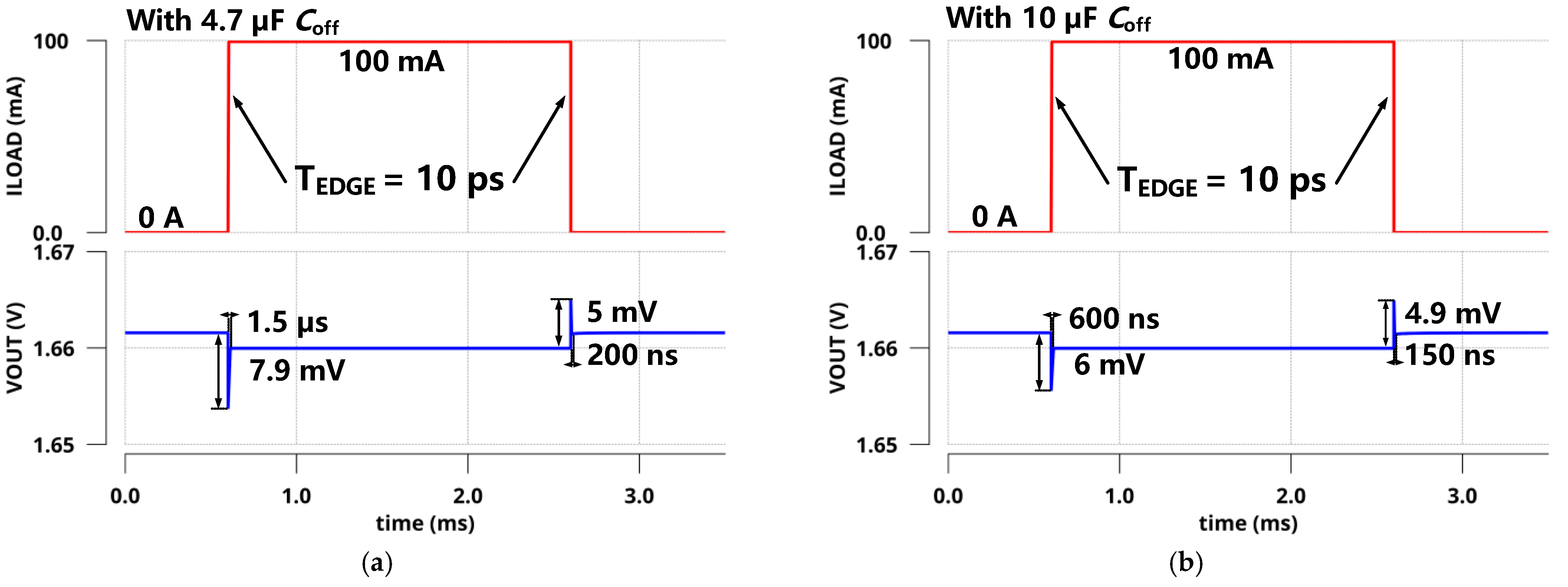
For the ESR case, a large off-chip capacitor of 1 µF with RESR = 100 mΩ was adopted for a large load current and better transient response. Figure 12 shows the Bode plots of the FVA loops at both zero and full load conditions (ILOAD = 0 µA and 100 mA). From the simulation, pout is pushed to low frequencies and becomes the dominant pole. At the zero load current condition, zESR and pgate are locked at frequencies higher than the loop UGB, resulting in a phase margin of 90°, as expected. At the full load current condition, pout shifted to higher frequencies owing to the decrease in output impedance. However, zESR could counteract the phase shift of pgate, and another internal pole pin was higher than UGB. Therefore, the phase margin at full condition is shown as 63.4°.
Figure 13 presents the PSR of the regulator at zero and full load conditions. With the introduction of Coff, PSR was significantly improved, especially at high frequencies. The simulated PSRs of the proposed LDO were −36 dB at 10 kHz and −46.3 dB at 1 GHz under a 100 mA load. Meanwhile, the PSR reached up to −50 dB at 10 kHz and −79.8 dB at 1 GHz under a zero load. Different load steps were applied and are shown in Figure 14 to confirm the transient response characteristics of VOUT within an edge time of 10 ps. When the load current changed from 0 µA to a moderate load (10 mA), as shown in Figure 14a, the undershoot and overshoot voltages were 2.4 mV and 1 mV, respectively. In addition, when the load current changed from zero load (0 µA) to a full load (100 mA), as shown in Figure 14b, the undershoot and overshoot voltages were 20.6 mV and 10 mV, respectively. The simulated load transient responses at other ESR conditions are shown in Figure 15. Obviously, this design could guarantee the stability of the system with good performance under the abovementioned conditions. From the simulation results, it is obvious that the transient response of the proposed LDO is significantly improved with the off-chip capacitor.
Figure 16 shows the quiescent current from −20 °C to 85 °C at different process corners and both zero and full current load conditions. Due to the high gate voltage of MP at the full load condition, the current replicated from the current mirror to the inverting amplifier is slightly reduced. It is obvious that there was a decrease in quiescent current at full load compared to the zero load condition. It reduced the loop gain at low frequencies slightly but did not deteriorate the circuit stability. Similarly, the quiescent current characteristics of the regulator with off-chip capacitors are illustrated in Figure 17. Due to the introduction of Coff, good transient characteristics can be realized without consuming a high current for a high UGB. As a result, the current efficiency is significantly improved. In addition, adaptive bias was adopted to improve the stability and load regulation of the system. Under a light current load, the adaptive bias consumes an ultra-low quiescent current. Meanwhile, under full current load, the increased current consumption is completely acceptable, as shown in Figure 17b.
To further verify the reliability of the transient response for the circuit, the undershoot voltage from −20 °C to 85 °C at different process corners is shown in Figure 18. When the load current changed from zero load to full load, load-transient undershoots could be observed. For the no off-chip capacitor case, the minimum undershoot was 124.6 mV at −20 °C, SS process, and the maximum undershoot was 178 mV at 85 °C, FF process. For a 1.65 V output voltage, the abovementioned undershoot voltage simulation results are acceptable with a quite small settling time. In addition, the load-transient undershoot results of the regulator with off-chip capacitors are illustrated in Figure 18b. The undershoot voltage is significantly reduced, with a minimum undershoot of 18 mV at −20 °C, SS process, and a maximum undershoot of 24.4 mV at 85 °C, FF process.
Simulation results of the 500-run Monte Carlo analysis for mismatch and process variations at −20 °C, 25 °C, and 85 °C are shown in Figure 19 and Figure 20. For the no off-chip capacitor case, the average undershoot µ is between 133 mV and 157 mV, and the standard deviation σ is approximately 2 mV. Moreover, for the off-chip capacitor case, as shown in Figure 20, the average undershoot µ is between 20 mV and 22 mV, and the standard deviation σ is approximately 420 µV.
To evaluate the speed of the transient response, an important parameter response time TR is defined in refs. [15,27]. For a fair evaluation, CL is replaced by the total capacitance adopted by the LDO CTotal, including the load capacitance and compensation capacitor. In the case that TEDGE is much smaller than TR, the current drawn from CL can be seen as a constant. It can be expressed as:
T R = C Total Δ V OUT Δ I OUT
Another estimation of TR is needed for fast LDOs in the case that TR < TEDGE. It reads:
T R = 2 C Total Δ V OUT T EDGE Δ I OUT
where TEDGE is the load-transient edge time. In addition, the figure of merit (FOM) defined in [17] is used as a baseline for LDOs, which is as follows:
FOM = K Δ V OUT ( I Q + I L M I N ) Δ I OUT
where K, IQ, and ILMIN are the ratio of the measured TEDGE to the minimum TEDGE, average value of quiescent current, and the minimum load current, respectively. Table 1 summarizes the comparison between the proposed FVA-based LDO and other state-of-the-art LDOs. For the no off-chip capacitor case, the TR of the design is not the smallest compared with other regulators. However, neither the transient characteristics nor the allowable range of the load capacitance meet the requirements of V/2 bias in cross-point memory [15]. For the regulator in [18], the parameter is obtained under the condition that the IL changes from 1 mA (not zero load) to the full load current. In addition, the proposed FVA-based LDO without Coff achieves the smallest FOM of 1.01 mV among previous works and can maintain stability over a wide range of load capacitances. For the off-chip capacitor condition, the transient response characteristics of the FVA-based LDO are also well improved. The smallest TR and FOM are achieved compared with other LDOs with Coff.

5. Conclusions

A fast-transient-response NMOS LDO with a wide load-capacitance range for cross-point memory was proposed. The fully integrated FVA-based LDO achieved a small undershoot voltage and a fast settling time within an edge time of 10 ps and a small FOM of 1.01 mV. For different selectors and memory devices, it could provide stable V/2 bias in the read operation within the load capacitance of 10 nF. This is the first attempt to propose an LDO for the V/2 bias scheme of cross-point memory. The limited on-chip output capacitor makes it suitable for SoC applications compared with FVF-based LDOs. Moreover, the proposed FVA-based LDO with a 1 µF off-chip capacitor shows a significantly improved performance, indicating that it is suitable for low-integration applications. In summary, the presented design achieved fast-transient-response characteristics and can remain stable with different load capacitances.

Author Contributions

Conceptualization, L.H. and X.L.; methodology, L.H.; software, X.L. and C.X.; validation, L.H., S.X. and G.P.; formal analysis, L.H.; investigation, L.H.; resources, X.L.; data curation, L.H.; writing—original draft preparation, L.H.; writing—review and editing, L.H., S.X., G.P. and X.L.; visualization, X.L. and C.X.; supervision, X.L., H.C. and Z.S.; project administration, Z.S. and X.L.; funding acquisition, Z.S. and X.L. All authors have read and agreed to the published version of the manuscript.

Funding

This work was supported by the National Natural Science Foundation of China (92164302, 440 91964204), Strategic Priority Research Program of the Chinese Academy of Sciences (XDB44010200).

Institutional Review Board Statement

Not applicable.

Informed Consent Statement

Not applicable.

Data Availability Statement

Not applicable.

Conflicts of Interest

The authors declare no conflict of interest.

References

  1. Intel Optane Solid State Drives Fill The Critical Storage Hierarchy Gap to Uniquely Deliver the Best Attributes of Both Memory and Storage. Available online: https://www.intel.com/content/www/us/en/products/docs/memory-storage/solid-state-drives/optane-ssds.html (accessed on 14 September 2022).
  2. Kau, D.; Tang, S.; Karpov, I.V.; Dodge, R.; Klehn, B.; Kalb, J.A.; Strand, J.; Diaz, A.; Leung, N.; Wu, J.; et al. A stackable cross point Phase Change Memory. In Proceedings of the 2009 IEEE International Electron Devices Meeting (IEDM), Baltimore, MD, USA, 7–9 December 2009; pp. 1–4. [Google Scholar]
  3. Chen, A. Analysis of Partial Bias Schemes for the Writing of Crossbar Memory Arrays. IEEE Trans. Electron Devices 2015, 62, 2845–2849. [Google Scholar] [CrossRef]
  4. Koo, Y.; Baek, K.; Hwang, H. Te-based amorphous binary OTS device with excellent selector characteristics for x-point memory applications. In Proceedings of the 2016 IEEE Symposium on VLSI Technology, Honolulu, HI, USA, 14–16 June 2016; pp. 1–2. [Google Scholar]
  5. Chen, A. Comprehensive methodology for the design and assessment of crossbar memory array with nonlinear and asymmetric selector devices. In Proceedings of the 2013 IEEE International Electron Devices Meeting (IEDM), Washington, DC, USA, 9–11 December 2013; pp. 30.3.1–30.3.4. [Google Scholar]
  6. Chen, A. A Highly Efficient and Scalable Model for Crossbar Arrays with Nonlinear Selectors. In Proceedings of the 2018 IEEE International Electron Devices Meeting (IEDM), San Francisco, CA, USA, 1–5 December 2018; pp. 37.2.1–37.2.4. [Google Scholar]
  7. Ciprut, A.; Friedman, E.G. Hybrid Write Bias Scheme for Non-Volatile Resistive Crossbar Arrays. In Proceedings of the 2018 IEEE International Symposium on Circuits and Systems (ISCAS), Florence, Italy, 27–30 May 2018; pp. 1–5. [Google Scholar]
  8. Lei, Y.; Liu, M.; Song, Z.; Chen, H. 2V/3 Bias Scheme with Enhanced Dynamic Read Performances for 3-D Cross Point PCM. In Proceedings of the 2020 IEEE International Symposium on Circuits and Systems (ISCAS), Seville, Spain, 12–14 October 2020; pp. 1–5. [Google Scholar]
  9. Jia, S.; Li, H.; Gotoh, T.; Longeaud, C.; Zhang, B.; Lyu, J.; Lv, S.; Zhu, M.; Song, Z.; Liu, Q.; et al. Ultrahigh drive current and large selectivity in GeS selector. Nat. Commun. 2020, 11, 4636. [Google Scholar] [CrossRef] [PubMed]
  10. Zhu, M.; Ren, K.; Song, Z. Ovonic threshold switching selectors for three-dimensional stackable phase-change memory. MRS Bull. 2019, 44, 715–720. [Google Scholar] [CrossRef]
  11. Lu, Y.; Ki, W.; Yue, C.P. 17. 11 A 0.65ns-response-time 3.01ps FOM fully-integrated low-dropout regulator with full-spectrum power-supply-rejection for wideband communication systems. In Proceedings of the 2014 IEEE International Solid-State Circuits Conference Digest of Technical Papers (ISSCC), San Francisco, CA, USA, 9–13 February 2014; pp. 306–307. [Google Scholar]
  12. Cai, G.; Lu, Y.; Zhan, C.; Martins, R.P. A Fully Integrated FVF LDO With Enhanced Full-Spectrum Power Supply Rejection. IEEE Trans. Power Electron. 2021, 36, 4326–4337. [Google Scholar] [CrossRef]
  13. Yoon, K.S.; Kim, H.S.; Qu, W.; Yuk, Y.S.; Cho, G.H. Fully integrated digitally assisted low-dropout regulator for a NAND flash memory system. IEEE Trans. Power Electron. 2017, 33, 388–406. [Google Scholar] [CrossRef]
  14. Choi, S.W.; Huh, Y.; Park, S.H.; Yoon, K.S.; Bang, J.S.; Shin, S.U.; Ju, Y.M.; Yang, Y.; Yoon, J.; Ahn, C.; et al. A quasi-digital ultra-fast capacitor-less low-dropout regulator based on comparator control for x8 current spike of PCRAM systems. In Proceedings of the 2018 IEEE Symposium on VLSI Circuits, Honolulu, HI, USA, 18–22 June 2018; pp. 107–108. [Google Scholar]
  15. Bu, S.; Guo, J.; Leung, K.N. A 200-ps-Response-Time Output-Capacitorless Low-Dropout Regulator With Unity-Gain Bandwidth >100 MHz in 130-nm CMOS. IEEE Trans. Power Electron. 2018, 33, 3232–3246. [Google Scholar] [CrossRef]
  16. Or, P.Y.; Leung, K.N. An Output-Capacitorless Low-Dropout Regulator With Direct Voltage-Spike Detection. IEEE J. Solid-State Circuits 2010, 45, 458–466. [Google Scholar] [CrossRef]
  17. Li, K.; Yang, C.; Guo, T.; Zheng, Y. A Multi-Loop Slew-Rate-Enhanced NMOS LDO Handling 1-A-Load-Current Step With Fast Transient for 5G Applications. IEEE J. Solid-State Circuits 2020, 55, 3076–3086. [Google Scholar] [CrossRef]
  18. Lu, Y.; Ki, W.-H.; Yue, C.P. An NMOS-LDO Regulated Switched-Capacitor DC–DC Converter With Fast-Response Adaptive-Phase Digital Control. IEEE Trans. Power Electron. 2016, 31, 1294–1303. [Google Scholar] [CrossRef]
  19. Mandal, D.; Desai, C.; Bakkaloglu, B.; Kiaei, S. Adaptively Biased Output Cap-Less NMOS LDO With 19 ns Settling Time. IEEE Trans. Circuits Syst. II Express Briefs 2019, 66, 167–171. [Google Scholar] [CrossRef]
  20. Magod, R.; Bakkaloglu, B.; Manandhar, S. A 1.24 µA Quiescent Current NMOS Low Dropout Regulator With Integrated Low-Power Oscillator-Driven Charge-Pump and Switched-Capacitor Pole Tracking Compensation. IEEE J. Solid-State Circuits 2018, 53, 2356–2367. [Google Scholar] [CrossRef]
  21. Lei, Y.; Chen, H.; Wang, Q.; Li, X.; Li, X.; Tian, Z.; Song, Z. A Single-Reference Parasitic-Matching Sensing Circuit for 3-D Cross Point PCM. IEEE Trans. Circuits Syst. II Express Briefs 2018, 5, 486–490. [Google Scholar] [CrossRef]
  22. Chien, W.C.; Yeh, C.W.; Bruce, R.L.; Cheng, H.Y.; Kuo, I.T.; Yang, C.H.; Ray, A.; Miyazoe, H.; Kim, W.; Carta, F.; et al. A Study on OTS-PCM Pillar Cell for 3-D Stackable Memory. IEEE Trans. Electron Devices 2018, 65, 5172–5179. [Google Scholar] [CrossRef]
  23. Lee, K.W.; Park, H.K.; Jung, S.-O. Adaptive Sensing Voltage Modulation Technique in Cross-Point OTS-PRAM. IEEE Trans. Very Large Scale Integr. Syst. 2021, 29, 631–642. [Google Scholar] [CrossRef]
  24. Chien, W.C.; Gignac, L.M.; Gong, N.; Yeh, C.W.; Yang, C.H.; Bruce, R.L.; Cheng, H.Y.; Papalia, J.M.; Miyazoe, H.; Cheng, C.W.; et al. Solution for PCM and OTS Intermixing on Cross-Point Phase Change Memory. In Proceedings of the 2019 IEEE 11th International Memory Workshop (IMW), Monterey, CA, USA, 12–15 May 2019; pp. 1–4. [Google Scholar]
  25. Man, T.Y.; Leung, K.N.; Leung, C.Y.; Mok, P.K.T.; Chan, M. Development of Single-Transistor-Control LDO Based on Flipped Voltage Follower for SoC. IEEE Trans. Circuits Syst. I Regul. Pap. 2008, 55, 1392–1401. [Google Scholar] [CrossRef] [Green Version]
  26. Al-Shyoukh, M.; Lee, H.; Perez, R. A Transient-Enhanced Low-Quiescent Current Low-Dropout Regulator With Buffer Impedance Attenuation. IEEE J. Solid-State Circuits 2007, 42, 1732–1742. [Google Scholar] [CrossRef] [Green Version]
  27. Hazucha, P.; Karnik, T.; Bloechel, B.A.; Parsons, C.; Finan, D.; Borkar, S. Area-efficient linear regulator with ultra-fast load regulation. IEEE J. Solid-State Circuits 2005, 40, 933–940. [Google Scholar] [CrossRef]
  28. Ming, X.; Liang, H.; Zhang, Z.-W.; Xin, Y.-L.; Qin, Y.; Wang, Z. A High-Efficiency and Fast-Transient Low-Dropout Regulator With Adaptive Pole Tracking Frequency Compensation Technique. IEEE Trans. Power Electron 2020, 35, 12401–12415. [Google Scholar] [CrossRef]
  29. Zhao, X.; Zhang, Q.; Xin, Y.; Li, S.; Yu, L. A High-Efficiency Fast-Transient LDO With Low-Impedance Transient-Current Enhanced Buffer. IEEE Trans. Power Electron. 2022, 37, 8976–8987. [Google Scholar] [CrossRef]
Figure 1. V/2 bias scheme for the read operation.
Sensors 22 09367 g001
Figure 2. The FVF-based LDO with single-transistor control (left) and inserted buffer (right).
Sensors 22 09367 g002
Figure 3. The FVA-based LDO with an inverting amplifier.
Sensors 22 09367 g003
Figure 4. FVF- and FVA-based LDOs with their pole-zero plots. (a) FVA LDO with R-C compensation. (b) FVA LDO with an off-chip capacitor.
Sensors 22 09367 g004
Figure 5. Transistor level schematic of the proposed FVA-based LDO.
Sensors 22 09367 g005
Figure 6. Function of the adaptive bias module.
Sensors 22 09367 g006
Figure 7. Bode plots of FVA loop responses with zero load capacitance.
Sensors 22 09367 g007
Figure 8. Phase margin of the FVA loop with a range of load capacitances from 0 pF to 10 nF.
Sensors 22 09367 g008
Figure 9. Simulated PSR of the proposed LDO with zero load capacitance.
Sensors 22 09367 g009
Figure 10. Simulated load transient responses with an on-chip capacitor of 0 and 100 pF within an edge time of 10 ps (a) CL = 0 pF; (b) CL = 100 pF.
Sensors 22 09367 g010
Figure 11. Simulated load transient responses compared with FVF-based LDO within an edge time of 10 ps and the on-chip capacitor of (a) CL = 0 pF; (b) CL = 100 pF.
Sensors 22 09367 g011
Figure 12. Bode plots of FVA loop responses with a 1 µF off-chip capacitor.
Sensors 22 09367 g012
Figure 13. Simulated PSR of the proposed LDO with a 1 µF off-chip capacitor.
Sensors 22 09367 g013
Figure 14. Simulated load transient responses with a 1 µF off-chip capacitor within an edge time of 10 ps for different load steps (a) ΔILoad = 10 mA; (b) ΔILoad = 100 mA.
Sensors 22 09367 g014
Figure 15. Simulated load transient responses within an edge time of 10 ps and load steps of 100 mA at different ESR conditions (a) Coff = 4.7 µF; (b) Coff = 10 µF.
Sensors 22 09367 g015
Figure 16. Quiescent current of the proposed LDO without Coff for different temperatures and process corners at zero and full current load conditions (a) at zero load; (b) at full load.
Sensors 22 09367 g016
Figure 17. Quiescent current of the proposed LDO with Coff for different temperatures and process corners at zero and full current load conditions (a) at zero load; (b) at full load.
Sensors 22 09367 g017
Figure 18. Simulated load-transient undershoots for different temperatures and process corners (a) without Coff; (b) with Coff.
Sensors 22 09367 g018
Figure 19. Monte-Carlo simulation results of load-transient undershoots without Coff for different temperatures (a) at −20 °C; (b) at 25 °C; and (c) at 85 °C.
Sensors 22 09367 g019
Figure 20. Monte-Carlo simulation results of load-transient undershoots with Coff for different temperatures (a) at −20 °C; (b) at 25 °C; and (c) at 85 °C.
Sensors 22 09367 g020
Table 1. Performance summary and comparison.
PublicationsTPE
2018 [15]
TPE
2021 [12]
TPE
2016 [18]
JSSC
2018 [20]
TPE
2020 [28]
TPE
2022 [29]
This Work
Technology0.13 µm65 nm65 nm0.25 µm0.18 µm0.18 µm0.11µm
Regulation FETPMOSPMOSNMOSNMOSPMOSPMOSNMOS
VIN (V)1–1.41.22.4–2.61.5–3.31.4–1.81.8–2.23.3
VOUT (V)0.8111.0–3.01.21.61.65
CLOn-chipOff-chipOn-chipOff-chip
0–25 pF300 pF30 pF1–47 µF4.7 µF1 µF0–1000 pF1 µF
ILMAX (mA)25203015015020010100
ILMIN (µA)120500100000
IQ (µA)11227–82101.24–10013.548708.5–12.5
CON-CHIP (pF)5.733033918.25N/AN/A482
PSR (dB@Hz)−5
@100 M
−16
@1 G
−12.8
@1 G
<−22
@20 k
−30
@10 k
−45
@10 k
−17.8
@1 G
−36
@10 k
TSETTLE (ns)<19020500 *9002000N/A50800
ΔVOUT (mV)32259195 *160207614420
TEDGE (ns)0.30.80.2105001000.01
K ratio308020100050,00010,0001
Charge pumpNoNoYesYesNoNoNo
TR (ns)0.210.90.253 *1066.76273800.69200
FOM (mV)52.913.91.3 *54756.8182.41.010.002
ResultsMeas.Meas.Meas.Meas.Meas.Meas.Sim.
* IL changes from 1 mA (not zero load) to 30 mA (full load).
Publisher’s Note: MDPI stays neutral with regard to jurisdictional claims in published maps and institutional affiliations.

