Abstract
This paper deals with developing and implementing a bidirectional galvanically isolated on-board charger of a high-power density. The power density of the new charger was 4 kW/kg and 2.46 kW/dm3, and the maximum efficiency was 96.4% at 3.4 kW. Due to the requirement to achieve a high-power density, a single-stage inverter topology was used. Regarding switching losses, due to the topology of the circuit with so-called hard switching, the switching frequency was set to 150 kHz. A laboratory prototype was built to verify the properties and operating principles of the described charger topology. The on-board charger has been tested in a microgrid test platform. Due to the parasitic properties of the transformer and other electronic components, overvoltage with subsequent oscillations occurred on the primary side of the transformer and damped resonance on its secondary side. These parasitic properties caused interference and especially voltage stress on the semiconductor elements. These undesirable phenomena have been eliminated by adding an active element to the charger topology and a new transistor control strategy. This new switching control strategy of transistors has been patented.
1. Introduction
Electromobility has become a growing global phenomenon. Not only it has the potential to contribute to the reduction of CO2 emissions and improve the environment, especially in large urban agglomerations [1], but it may also provide a solution to the problem of limited fossil fuel reserves. The advances in electromobility concern both passenger cars as well as public transport (electric buses and trolleybuses with battery backup). However, these developments are also accompanied by problematic power engineering and operational character aspects. For the smooth incorporation of electric vehicles, it is necessary to ensure that there is enough electricity and sufficient transmission capacity in the power grid to charge electric vehicles (EVs) when needed or to optimise the charging mode of a significant proportion of EVs so that the electricity sources and distribution grids are able to cover the demand [2].
The battery charging time is significantly longer than the refuelling time of a conventional car [3]. Charging times range from tens of minutes to tens of hours, depending on the specific vehicle type, the battery itself and the charging station [4]. Fast charging is limited, among other things, by the need for high power consumption from the grid and the capacity of the distribution grid at a particular place and time. This problem is solved, for example, by including a battery in the charging station to cover significant power peaks to ensure the fast charging of an EV [5]. The battery in the charger increases its cost, and the temporary energy storage in it reduces the whole system’s efficiency. Currently, several proposed charging-in-motion concepts are associated with several technical and operational problems and have not been widely applied commercially [6].
Currently, the electricity sector is developing the so-called smart grids, enabling a more intense and efficient use of energy sources and distribution grids and better control of their capacity. The implementation of smart grids is currently revolutionizing the distribution and storage of electricity and affecting its generation and consumption [7,8,9].
At the same time, there is a growing importance of renewable sources of electricity, whose performance is in many cases uneven, depending on the actual wind or sunshine, which cannot be influenced, only predicted to a limited extent [10]. Therefore, the need for electricity storage will also increase, which is estimated to triple by 2030 compared to the current situation [11]. One option for short-term electricity storage is to use the battery pack of an electric vehicle connected to the grid via a bidirectional charging station [11,12,13,14]. Such a bi-directional charger can also be designed as a power conditioner [15].
Using EV batteries to support the grid is beneficial only if large EV population is involved [16] and intelligent charging scheduling is also useful [17], which is easier when dealing with a large number of single-owner vehicles. It is therefore desirable to include, for example, huge fleets of public transport EV, such as electric buses, or car-sharing fleets. It was also established that drivers are more open to adopting e-mobility after becoming familiar with the concept through car-sharing. At the same time, easy charging availability is an important factor for EV use, even if it is shared [18,19] The bi-directional on-board charger can find a use in all these applications.
The currently used chargers can be classified according to several criteria. Practically all used chargers must be designed and controlled to respect the limits of current harmonic distortion and power factor [5,20]. Besides the fact that galvanically isolated chargers provide a higher level of safety, their disadvantage is that the transformer increases its weight, size and cost. Moreover, the transformer decreases the overall efficiency of the device. For example, in a galvanically isolated charger operating at 200 kHz, transformer losses are 20% of the total losses [21]. From the point of view of losses, it would be more advantageous to operate the transformer and switch elements at low frequency [22,23].
Many circuit designs allow for a bidirectional power flow with harmonic grid current. One of the simplest is called “totem pole PFC” [24]. It does not contain a transformer, with all consequent advantages and disadvantages (lower power losses, weight, cost, lower level of safety). Furthermore, the battery voltage must always be higher than the main voltage amplitude in both power flow directions. Therefore, it is not a suitable solution for our purpose.
Series connection of a rectifier with DC/DC converter creates a charger with the so-called two-stage energy transfer [25]. Using this topology in the charging mode, the active front-end rectifier with the sinusoidal current consumption rectifies the input AC voltage. The resulting DC link voltage is converted via an isolated DC/DC converter with an insulating high-frequency (HF) transformer. All the high-power switches need to work with high switching frequency, which causes switching losses proportional to the transmitted power and control technique.
To reduce switching losses, different topologies were proposed utilizing a zero-voltage switching [26] or resonant effects, for example [27]. Other strategies to reduce power losses of the charger are to reduce the number of energy conversions, reduce the number of HF power switches and passive components that cause losses and increase the weight, dimensions and also price of the device.
The number of energy conversions is reduced in topologies based on the principle of the matrix converter; this convertor is called single stage [25,28]. This converter supports direct conversion of AC voltage to AC voltage with different parameters. Such energy is subsequently transformed and rectified. This removes the need for DC bus intermediate stage. Input and output bridges work synchronously on the same frequency. All used power switches are switched with high-frequency, and their parameters need to reflect it. HF transistors are characterised with higher RDS in on-state and the higher forward voltage drop across the body diode.
It is possible to reduce the number of HF switches by optimizing the circuit topology but keeping the single stage energy conversion. The mentioned topologies and their relationship are given in [29].
The resulting circuit and its operation are very well described, for example, in [30]. A similar principle was also proposed for a high-power railway application in [31,32].
The circuit in Figure 1 is based on the topology given in [32,33]. Inductor L is used for energy accumulation in order to be able to transfer the energy from the primary to the secondary side under different magnitudes of ud.
The selected topology provides galvanic isolation between the mains and battery sides of the charger’s circuit. Furthermore, it will comply with the following requirements: high-power density, lower number of components, absence of bulky and unreliable electrolytic capacitors, smaller size and lower weight, higher reliability, lower circuit complexity, good dynamic performance, lower harmonic content, high efficiency and lower price in comparison with other typically used topologies.
Other concepts of bidirectional converters to be utilised in bidirectional chargers can be found in [34].
The contribution of this work can be summarised as follows:
- A description of the implementation of the first prototype and its problems related to the circuit topology and parasitic properties of the elements encountered and their solutions not reported in the literature;
- Describe the elimination of voltage spikes using passive disconnectors (RCDs) proved inappropriate due to the significant power losses;
- The introduction of an innovative approach that eliminates voltage spikes based on the use of an applied active clamp in this situation;
- Proposed and described a switching control method that eliminates unwanted HF oscillations on both the primary and secondary sides of the transformer in the on-board charger;
- Description of the development, implementation and testing of a bidirectional charger with galvanic isolation, whose parameters were 4 kW/kg and 2.46 kW/dm3 and the maximum power of the charger is 7.2 kW, which uses a switching frequency of 150 kHz.
For comparison, comparable power converters reported in the literature achieve power density of 0.65 kW/dm3 [35], 1.875 kW/dm3 [36] (gravimetric densities are not specified), 2 kW/dm3 with 1.2 kW/kg [37] and 2.44 kW/dm3 (gravimetric density is not specified) [38].

Figure 1.
Bidirectional single-stage charger topology [33,39].
This paper is organised as follows. Section 2 deals with the characteristics of the first charger prototype. The relationships for the design of the storage choke are also derived. Section 3 focuses on solving the overvoltage and oscillation problems in the prototype. Relations for calculating the value of the surge eliminating capacitor are given, including the timing of its switching. The simulations were used to check the correctness of the proposed solution set-up. The logic signal waveforms for charging and discharging modes are shown. Section 4 describes the second prototype of the bidirectional charger, including the surge and oscillation suppression circuit. Section 5 described the platform where the on-board charge was laboratory tested. Finally, Section 6 describes the measurements on the second prototype, including the measurement results.
2. Verification of Selected Topology of Bidirectional Charger
When we compare the characteristics of the different topologies of inverters suitable for implementing on-board bidirectional chargers for electric vehicles, the best option seems to be the topology, as shown in Figure 1 [33,39].
2.1. Calculation of Accumulating Inductor Inductance
To derive inductance of accumulating inductor, Figure 1 and Figure 2 are considered. The primary purpose of the inductor is to accumulate energy in charging mode, where together with bridge Q5 to Q8 it forms the so-called boost converter. The switching frequency of transistors Q5 to Q8 is many times higher than mains frequency. For this reason, the voltage ud might be considered constant during a single switching period of these transistors.
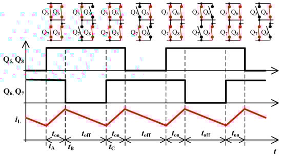
Figure 2.
Principle of selected topology from Figure 1 in charging mode. Top-down: waveforms of control pulses Q5, Q8, control pulses Q6, Q7, inductor current iL.
In time interval ton the energy is accumulated in inductor L. Voltage ud is applied to it and inductor current starts to rise. In time toff, inductor supplies energy into the battery through the transformer and its current starts to decrease. In time toff the inductor voltage is equal to the battery voltage multiplied by transformer ratio k and reduced by voltage ud. The inductor shall be designed so that its current ripple is below the limit. The following equations apply:
where k = 1.33 is the transformer ratio.
Figure 2 implies the equation for the inductor current period:
Combining (1), (2) and (3), the equations below are derived:
Combining (1), (3) and (6), the equation below is derived:
Equation (7) can be used to derive the equation for inductance:
The switching frequency of the charger is 150 kHz. For a ripple current of 10 A, a choke inductance of 45 μH was calculated according to Equation (8). Due to the fact that at this inductance value, the inductor’s core was oversaturated, a value of 25 μH was finally chosen experimentally. For this inductance, its ripple current reaches up to 20 A.
2.2. Experimental Results Measured on the First Prototype of Bidirectional Charger
To verify the selected topology of the charger and its proposed control principles, a laboratory prototype was built.
The prototype was assembled from three separate printed circuit boards: control, driver and power. The control board contains:
- Microcontroller EFM8LB12F64E-QFP32 from Silicon Labs.
- Supporting circuits for logic of control pulses and elimination of various switching failure modes.
- Regulated power supplies with various output voltages.
The power board contains:
- Power transistors, capacitors, planar transformer and inductor. With respect to the required dimensions and overall weight of the device cores, E64/10/50-3F36 and PLT64/50/5-3F36 were used. A detailed list of the used components is given in Section 4.
Figure 3 shows the first prototype of the single stage bi-directional isolated on-board charger with its three PCBs in sandwich-like assembly.
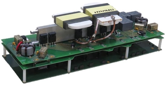
Figure 3.
A photograph of the first prototype of the bidirectional isolated on-board charger.
The waveforms in Figure 4 show transient phenomena in the circuit during two switching periods. After the switch-off of the first transistor pair Q5, Q8, the voltage starts to rise (Figure 4, point 1) on the primary side of the transformer and at the same time also, its current starts to rise. Transformer TR (see Figure 1) is not able to immediately pass the inductor L current due to its leakage inductance. This causes overvoltage followed by oscillations (Figure 4, point 2). The energy transfer through the transformer ends when all transistors Q5 to Q8 have switched on again.
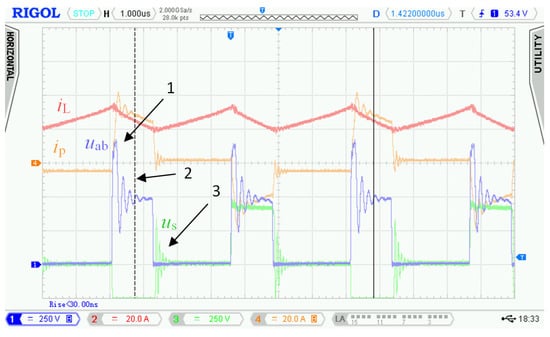
Figure 4.
Waveforms measured with the first prototype of bidirectional charger in charging mode. Measured at: ud = 175.5 V, id = 25.8 A, uBAT = 397 V, iBAT = 9.95 A, PBAT = 3950 W and inductor inductance L = 25 μH.
After the primary voltage of the transformer decreases to zero volts, a decrease in its secondary side voltage follows. A steep decrease in the secondary voltage induces dumped oscillations due to parasitic circuit properties (Figure 4, point 3). Overvoltage and oscillations are not only the source of EMI noise but cause voltage to overstress to power transistors, which could lead to their destruction. For this reason, we had to find a solution to eliminate the oscillations and reduce the overvoltage.
3. Selected Topology Troubleshooting
In Figure 5 there is a principal scheme of the bidirectional charger, to which relate all the following descriptions of logic signals of transistor Q1 to Q13 and all experimental measurements.
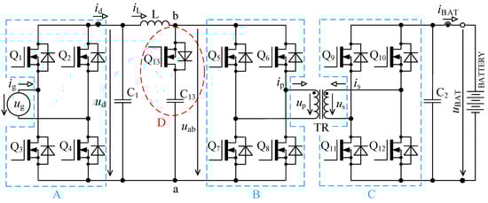
Figure 5.
Topology of bidirectional charger extended with an active element “D” consisting of a transistor Q13 and capacitor C13.
As was already described in Section 2, using the bidirectional topology charger from Figure 1 and driving transistors according to Figure 2, there are two major issues:
Overshoot of voltage up (Figure 4, point 1) and oscillations (Figure 4, point 2) on the primary winding of transformer TR caused by its parasitic properties.
Damped resonance of parasitic circuit elements on the secondary side of the transformer (Figure 4, point 3) caused by steep decrease in primary voltage up.
The first problem with voltage up overshoots was successfully solved by implementing an active circuit element marked “D” in Figure 5 and its exact timing. This active element consists of series connection of transistor Q13 with capacitor C13. Transistor Q13 switches in the capacitor C13 at exactly defined time period.
The second problem with damped resonance of parasitic circuit elements on the secondary side of the transformer was eliminated by a different control technique of transistors Q9 to Q13 (different to the control shown in Figure 2).
3.1. Root Cause Description of Overvoltage on the Primary Side of Transformer and Solution
When the transistor pair Q5, Q8 or Q6, Q8 is switched off, inductor L acts as a source of constant current. In the ideal case, this current would start to flow through the primary winding of transformer, but its leakage inductance prevents that. In case the active element “D” (see Figure 5) is missing, the current will not have a path to flow, and voltage will rise between nodes a and b. This would lead to severe overvoltage.
The moment of switching off the transistor pair Q5, Q8 or Q6, Q7 could be described based on Figure 6, which represents circuit schemes in simulation software Microcap, which was used to verify the circuit behaviour.
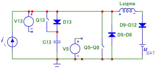
Figure 6.
Equivalent scheme for simulation of transient effect with active control of capacitor C13.
At the moment of switching off transistor pair Q5, Q8 (Q6, Q7), the transistor Q13 is also switched off. See Figure 2, time t0 (t0 + ½T). The inductor current iL flows immediately through internal body diode D13. For the purpose of simplification, its magnitude could be considered constant over the duration of transient. At the same time, the current through leakage inductance Lsigma starts to rise. In time t1 (t1 + ½T) transistor Q13 turns on.
Capacitor C13 and leakage inductance Lsigma together form a resonant circuit. Its resonant frequency is given by (9).
During the transient, the energy accumulated in inductance Lsigma is:
The same amount of energy accumulates in the capacitor C13, which is based on the general knowledge about the behaviour of resonant LC circuits:
Let us assume that in t0 the capacitor C13 is charged to voltage k·uBAT from the previous period, where k is transformer ratio. The following equation is obtained using (10) and (11):
Neglecting the voltage drop across the body diode D13 and transistor Q13 (see Figure 5), Equation uC13max = uabmax applies. If the maximum uabmax voltage is specified (for example based on breakdown voltage of semiconductors), required C13 capacity can be calculated as:
For the capacitor C13 to remain charged to a voltage of magnitude k·uBAT during the end of the transient effect, exactly one-half period of resonant effect needs to occur. In time t0, charging of capacitor occurs through diode D13. Discharging occurs through transistor Q13, which needs to be turned off at specific time. The total time of current conduction through the capacitor must be half of the period of the resonant frequency.
Time tQ13 cannot be longer than the switch-off duration of one of the transistor pairs from bridge “B”, further reduced by safety margin time tdelay, which corresponds to (½T − tov − tdelay). In that case, the time tQ13 is shorter compared to (14):
For time interval when tov < (½T − tdelay), (14) applies.
For time interval when tov ≥ (½T − tdelay), (15) applies.
It is desirable to design the capacitance of C13 so that there is no voltage breakdown of semiconductors during the maximum instantaneous current iL magnitude and during maximum battery voltage.
It was decided that the highest voltage amplitude uabmax is in the range 650 V to 700 V. Review of parameters for which C13 was designed:
Leakage inductance Lsigma of used transformer is 1 μH, maximum battery voltage is 420 V, transformer ratio is 1.33, maximum inductor current amplitude iL is below 50 A.
For the given voltage uabmax amplitude, the C13 capacitance was calculated according to (13) in the range from 125 nF to 308 nF. Capacity 270 nF was chosen, for which the duration was calculated as tQ13 = 1632 ns. The calculations were verified by simulations, see Figure 6.
Inductor L is replaced with a constant current source iL in the scheme above. Its value can either be set as a constant value or as a periodic triangular waveform. Transistors were replaced by switches controlled by voltage sources (V5 to V13) with configurable switching diagram. A switch marked as Q5 to Q8 substitutes transistors of bridge “B”, and diode D5 to D8 represents their body diodes.
The purpose of the first simulation was to verify the amplitude voltage spike during maximum current iL = 50 A and maximum battery voltage uBAT = 420 V. Simulation is performed for 150 kHz inverter switching frequency therefore 300 kHz frequency of inductor current, Lsigma = 1 μH, C13 = 270 nF. Current source iL supplies constant current with magnitude 50 A. Time tQ13 was configured to be 1632 ns.
Simulated waveforms of voltages and currents are shown in Figure 7. Substituting the values into (13) the resultant voltage amplitude of uabmax = 656.2 V. From the simulation results, the value of 654.4 V was obtained. This is almost a full match to the calculated value.
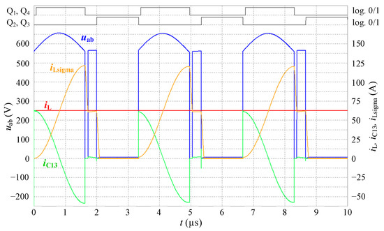
Figure 7.
Waveforms of voltages and currents during transient effect as simulated in Microcap software for uBAT = 420 V, iL = 50 A, tQ13 = 1632 ns, tov = 1327 ns, tdelay = 70 ns.
Another simulation was performed in order to confirm the correctness of (9) to (15) and the overall functionality of the proposed solution. Specific values of voltages and currents, which were measured during experimental measurements with bidirectional charger, were simulated.
The following parameters are considered:
Periodic waveform iL of triangular shape with values iLmin = 24 A, iLmax = 43 A, uBAT = 371 V. The tov overlap time was 1833 ns. The switch-off time interval of the transistor pair of bridge “B” was 1430 ns, for this reason, according to (15), the time tQ13 was shortened to 1430 ns.
The simulation result is shown in Figure 8. The experimentally measured values are shown in Section 6. The simulated and experimentally measured waveforms clearly show the agreement. The simulations also verified the correctness of the derived equations.
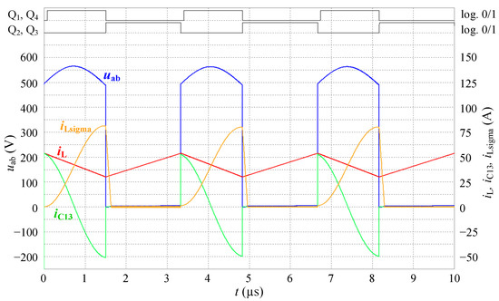
Figure 8.
Waveforms of voltages and currents of transient effect as simulated in Microcap software for values uBAT = 371 V, iLmin = 24 A, iLmax = 43 A, tQ13 = 1430 ns, tov = 1833 ns, tdelay = 70 ns.
3.2. Principle of the New Strategy of Bidirectional Charger Control in the Charging Mode
In order to achieve higher efficiency, transistors Q1 to Q4 (bridge “A”) are actively driven with mains frequency 50 Hz and work as an active rectifier. Transistors Q1 to Q4 always switch in pairs Q1, Q4 and Q2, Q3. Correct switching of those transistor pairs is dependent on the polarity of instantaneous mains voltage and is activated after zero crossing.
Switching period T is in the order of units of μs, which relates to switching frequency in order of hundreds of kHz. Switching period for transistor Q13 is two times shorter (twice the frequency). Transistors Q5 to Q8 (bridge “B”) always switch on all together during energy accumulation into inductor L and during the energy transfer the pair Q5, Q8, or Q6, Q7 is switched on. For the following explanations, it is assumed that time t0 starts a new period when the energy transfer from inductor L through transformer TR (see Figure 5) into the battery occurs. The circuit is in a dynamically stabilised state from the previous period. Energy is accumulated in inductors and capacitors.
Specific switching time intervals for transistors Q5 to Q13 for charging and discharging mode are described below. Logic diagrams of these transistors switching are shown in Figure 9 for better clarity. Figure 10 shows experimentally acquired waveforms of voltages and current in specific time intervals. All these waveforms are relevant only for charging mode. Important parameter in charging mode is overlap duration tov. During this time, all four transistors Q5 to Q8 are switched on and energy is being accumulated into inductor L. Duration marked as tdelay is achieved with shifting of microcontroller timers.
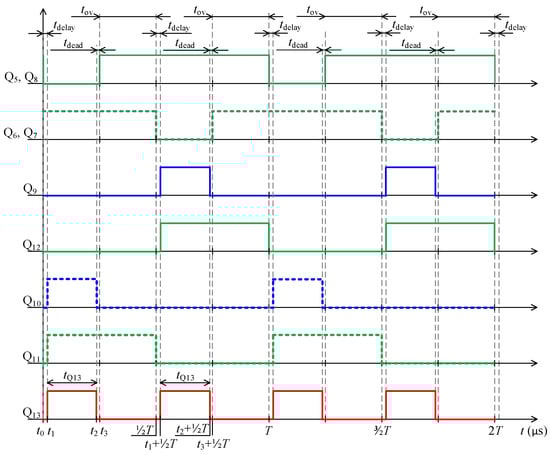
Figure 9.
Waveforms of control signals for charging cycle.
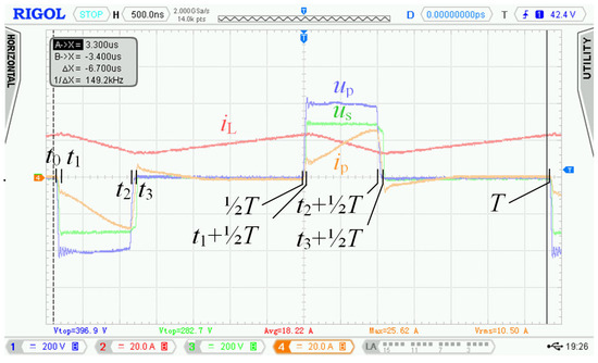
Figure 10.
Experimentally acquired waveforms during charging mode; time interval t0 ≤ t ≤ T, where tov = ⅜T.
This duration needs to be applied when transistors Q9 to Q12 are actively driven due to a delay in energy transfer from the primary to the secondary winding of the transformer. Duration of tdelay needs to be long enough to guarantee that voltage generated on the secondary winding is higher than the battery voltage uBAT. Without tdelay the current would flow from the battery through transistor pair Q9, Q12 or Q10, Q11 first, and later it would be overdriven by current generated in the transformer’s secondary winding. Time interval marked as tdead guarantees reliable turn off of all transistors connected in common part of the circuit. It shall never occur that transistors Q9 and Q11 or Q10 and Q12 switch on at the same time.
3.2.1. Time Interval t0 ≤ t < t1
In time t0 transistor pair Q5, Q8 was turned off while transistors Q6, Q7 remained turned on from the previous period. Transistor Q13 is turned off. Additionally, transistor Q12 was turned off. All the transistors in bridge “C” are turned off. The explanation refers to Figure 9, Figure 10 and Figure 11.
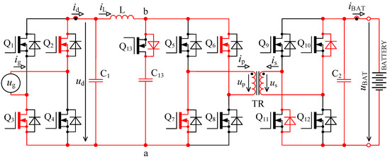
Figure 11.
Charging mode–time interval t0 ≤ t < t1.
Current iL flows through inductor L while the primary winding current ip of transformer TR is zero. In an ideal case, the inductor L current should immediately flow into the primary winding of transformer TR, but this is not possible due to its leakage inductance. Inductor current iL continues through the body diode of transistor Q13 into capacitor C13, which charges up and accumulates energy. In case of C13 absence, the voltage between a and b nodes would rise to dangerous overvoltage, leading to transistor destruction. The active element, composed of a series connection of transistor Q13 and capacitor C13, prevents that. Current is, which is induced by current increase ip, is flowing back through the body diodes of transistors Q10 and Q11. In this time the, bridge “C” works as a passive diode bridge rectifier.
3.2.2. Time Interval t1 ≤ t < t2
The time t1 (tdelay) is very short, i.e., units of percent of the switching period (150 kHz). In this case, it was 100 ns. The explanation refers to Figure 9, Figure 10 and Figure 12. The primary purpose of this t1 is to add two safety delays:
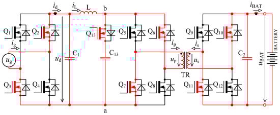
Figure 12.
Charging mode–time interval t1 ≤ t < t2.
- Between switching off transistor pair Q5, Q8 and switching on Q3, while transistors Q6, Q7 remain switched off. Simultaneous switching on of all transistors in bridge “B” would mean short circuit of capacitor C13.
- Guarantees that voltage generated across the secondary winding of the transformer is greater than battery voltage uBAT.
In time t1 transistors Q10, Q11 and Q13 turn on. Current ip is rising and is now given by the difference of currents iL and capacitor current iC13. After some time, both currents iL and ip equalise and in this moment direction of current through C13 reverses. The energy which was accumulated in C13 is now being discharged into transformer TR. Current ip is now given by the sum of capacitor iC13 and inductor iL currents. In this time interval, the energy is transferred from the primary to the secondary winding of transformer TR. Transistors Q10 and Q11 were turned on to reduce losses during the secondary current flow.
3.2.3. Time Interval t2 ≤ t < t3
In time t2 transistors Q10 and Q13 were turned off, while the capacitor C13 was disconnected from the bridge “B”. The current ip dropped. The leakage inductance of the transformer tries to keep its current magnitude. For this reason, the polarity of up is reversed, but body diodes of transistors Q5 and Q8 clamp the voltage to approximately zero. The explanation refers to Figure 9, Figure 10 and Figure 13.
Figure 13.
Charging mode–time interval t2 ≤ t < t3.
Considering that in time t2 transistor Q10 is turned off, the energy accumulated in the leakage inductance of transformer keeps up the current is, which flows through Q10 body diode.
3.2.4. Time Interval t3 ≤ t < ½T
In t3 instant, the transistors Q5 and Q8 were turned on, while transistors Q6, Q7 and Q11 remained turned on. Transistors Q5, Q8 are turned on at zero voltage, which was reached during the previous time interval.
The primary winding of transformer TR is shorted out with transistors Q5 to Q8, current ip decreases to zero. The instantaneous voltage of rectified grid voltage ud is now connected to inductor L, its current rises, and energy is being accumulated. The accumulation phase remains till ½T. The time during which the energy is being accumulated into the inductor is marked as tov.
In order to increase the amount of energy accumulated in inductor L, which is transferred to the secondary winding of transfer, the overlap duration tov needs to be extended while t3 and t2 shortened.
During the accumulation period, the transistor Q11 from bridge “C” remains turned on and, together with the body diode of transistor Q12 keeps the secondary voltage us close to zero till the moment when no more energy is transferred into the battery. The explanation refers to Figure 9, Figure 10 and Figure 14.
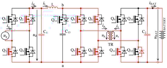
Figure 14.
Charging mode–time interval t3 ≤ t < ½T.
3.2.5. Time Interval ½T ≤ t < (t1 + ½T)
Time ½T is half of the switching period when everything starts to repeat. The main difference is that transistor pairs Q5, Q8 and Q6, Q7 switched their roles.
In time ½T transistor pair Q6, Q7 was turned off, while transistors Q5, Q8 remained turned on from the previous period. Transistor Q13 is turned off. Furthermore, transistor Q11 was turned off. All the transistors from bridge “C” are now turned off. Waveforms of voltages and currents are analogous to what was described in Section 3.2.1.
3.2.6. Time Interval (t1 + ½T) ≤ t < (t2 + ½T)
In time (t1 + ½T), transistors Q9, Q12 and Q13 were turned on. Transistors Q9, and Q12 were turned on in order to reduce conduction losses during the secondary current flow. Waveforms of voltages and currents are analogous to what was described in Section 3.2.2.
3.2.7. Time Interval (t2 + ½T) ≤ t < (t3 + ½T)
In time (t2 + ½T), transistors Q9 and Q13 were turned off. Transistors Q5, Q8 and Q12 remained turned on. Waveforms of voltages and currents are analogous to what was described in Section 3.2.3.
3.2.8. Time Interval (t3 + ½T) ≤ t < T
In time (t3 + ½T), transistors Q6 and Q7 were turned on. Transistors Q5, Q8 and Q12 remained turned on. Waveforms of voltages and currents are analogous to what was described in Section 3.2.4.
3.3. Principle of the New Strategy of Bidirectional Charger Control in the Discharging Mode
In discharging mode of a bidirectional charger, transistors Q1 to Q4 (bridge “A” in Figure 5) and transistors Q9 to Q12 (bridge “C” in Figure 5) work as inverters. Transistors Q5 to Q8 (see bridge “B” in Figure 5) work as rectifiers. Transistors Q9 to Q12 chop the direct voltage of battery uBAT into AC voltage, which is later transformed by transformer TR and actively rectified by transistors Q5 to Q8.
The voltage ud itself does not have a constant magnitude, but it is modulated with change of ton parameter in such a way that it resembles rectified sine wave. Change of ton is realised by switching on the duration of transistor pairs Q9, Q12 or Q10, Q11 (inverter “C” in Figure 5), while transistors Q12 and Q11 are switched on for the whole duration of switching half-period. Only after tdelay transistor pairs Q5, Q8 or Q6, Q7 (inverter “B” in Figure 5) are switched on.
The function of inverter “A” is to toggle the polarity of direct pulsing voltage ud so that it reflects the actual polarity in power grid and thus allows the energy to flow from the battery into power grid.
Labelling of transformer windings is kept the same as in charging mode in the Subsection B. Winding of transformer on the battery side is labelled as the secondary winding even though its function in discharging mode is inverted.
Switching period T has μs unit, which reflects the switching frequency in the order of hundreds of kHz. The switching frequency of 150 kHz is used in the example below.
In the following example, it is assumed that time t0 is the start of a new period and that the circuit is in a dynamically stabilised state from the previous period, inductors and capacitors have accumulated energy. For clarity, Figure 15 shows the logic switching waveforms of transistors. Figure 16 and Figure 17 show experimentally acquired waveforms of voltages and currents in specific time instants. All those waveforms are relevant only for discharging mode. The main parameter for discharging mode is marked as ton. During this time one of the transistor pairs Q9, Q12 or Q10, Q11 is switched on and energy is transferred via transformer TR and inverter “B” and “A” into power grid. Duration marked as tdelay for switching of transistor Q13 is realised by a phase shift of timer of microcontroller and for transistors Q5 to Q8 by utilizing tdead in the microcontroller.
Figure 15.
Waveforms of control signals for discharging cycle, ton = ¼T.
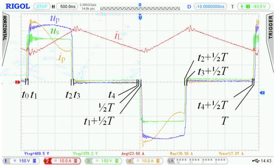
Figure 16.
Experimental measurement in discharging mode–time interval t0 ≤ t < T, part a.
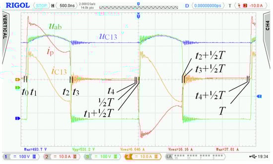
Figure 17.
Experimental measurement in discharging mode-time interval t0 ≤ t < T, part b.
Voltage spikes are reduced with capacitor C13, first passively and later after tdelay through switched-on transistor Q13. In the specific moment, the accumulated energy of C13 discharges back into the circuit through switched-on transistor Q13.
3.3.1. Time Interval t0 ≤ t < t1
In moment t0, transistors Q9, Q12 are turned on. Transistors Q5 to Q8, Q10, Q11 remain turned off. The secondary side of the transformer TR is connected to battery voltage uBAT. Due to this, the secondary and later also the primary current starts to flow through the transformer TR, which causes voltage up to rise. Current ip flows back through the body diodes of transistors Q5 and Q8. The explanation refers to Figure 15, Figure 16, Figure 17 and Figure 18.
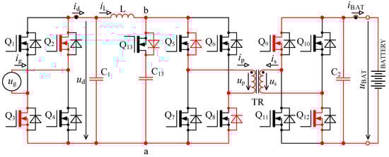
Figure 18.
Discharging mode–time interval t0 ≤ t < t1.
Primary voltage up reaches the magnitude which corresponds to the product of battery voltage and transformer TR transforming ratio. If the voltage up exceeds the voltage of capacitor C13, the current starts to flow through the body diode of transistor Q13, and capacitor C13 is charging. At this moment, energy is transferred into power grid and capacitor C13.
3.3.2. Time Interval t1 ≤ t < t2
In time instant t1 transistors Q5, Q8, Q13 are turned on to reduce conduction losses across their body diodes. The delay of switching on the transistors tdelay is implemented due to the leakage inductance of transformer TR. Voltage up is greater than instantaneous voltage ud, and inductor current iL is rising. Capacitor C13 is charging, and its current decreases. In a moment when the currents ip and iL have the same magnitude, the current’s direction through C13 reverses and its accumulated energy starts to discharge. Current iL is now determined by the sum of capacitor current iC13 and current ip. The explanation refers to Figure 15, Figure 16 and Figure 17 and Figure 19.
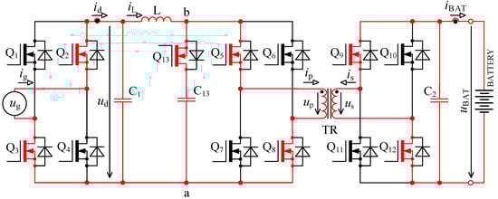
Figure 19.
Discharging mode–time interval t1 ≤ t < t2.
3.3.3. Time Interval t2 ≤ t < t3
In time instant t2, transistors Q9 and Q13 are turned off. The secondary current is must maintain its direction and flows through the body diode of transistor Q11. At the same time, the transistor Q13 current is interrupted. Next, the current ip drops. Transformer leakage inductance tries to maintain the current through the transformer ip magnitude. This causes a decrease in up voltage. The explanation refers to Figure 15, Figure 16 and Figure 17 and Figure 20.
Figure 20.
Discharging mode–time interval t2 ≤ t < t3.
3.3.4. Time Interval t3 ≤ t < t4
In time instant t3 transistors Q5 and Q8 are turned off. Inductor current iL maintains its direction even after the end of energy transfer from the transformer. Current iL flows back through the body diodes of transistors Q5 to Q8. This keeps the primary winding of transformer TR voltage close to zero. The explanation refers to Figure 15, Figure 16 and Figure 17 and Figure 21.
Figure 21.
Discharging mode–time interval t3; discharging mode–time interval t4 ≤ t < ½T. t < t4.
3.3.5. Time Interval t4 ≤ t < ½T
In time instant t4, the energy accumulated in the leakage inductance of the secondary winding is depleted and, therefore, the transistor Q12 is turned off. Other transistors were already turned off in the previous time interval. This allows zero current switching on during the next time interval. The explanation refers to Figure 15, Figure 16 and Figure 17 and Figure 22.
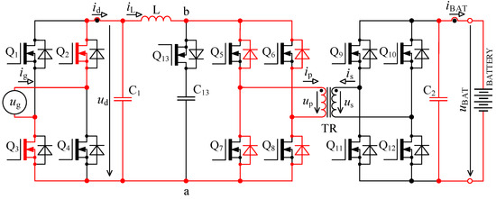
Figure 22.
Discharging mode–time interval t4 ≤ t < ½T.
3.3.6. Time Interval ½T ≤ t < (t1 + ½T)
In time instant ½T transistors Q10, Q11 are turned on, and transistors Q5 to Q8, Q10, Q11 remain turned on. Current ip flows back through the body diodes of transistors Q6 and Q7. If the voltage up exceeds the magnitude of capacitor C13 voltage, the current through the body diode of transistor Q13 starts to charge the capacitor C13. Waveforms of voltages and currents are analogous to what was described in Section 3.3.1.
3.3.7. Time Interval (t1 + ½T) ≤ t < (t2 + ½T)
In time instant (t1 + ½T), transistors Q6, Q7 and Q13 are turned on, and energy from the battery is transferred into power grid. Waveforms of voltages and currents are analogous to what was described in Section 3.3.2.
3.3.8. Time Interval (t2 + ½T) ≤ t < (t3 + ½T)
In time instant (t2 + ½T), transistors Q10 and Q13 are turned off. The secondary current is must maintain its direction and flows back through the body diode of transistor Q12. At the same time, the transistor Q13 current is interrupted. Waveforms of voltages and currents are analogous to what was described in Section 3.3.3.
3.3.9. Time Interval (t3 + ½T) ≤ t < (t4 + ½T)
In time instant (t3 + ½T), transistors Q6 and Q7 are turned off. Current iL flows back through the body diodes of transistors Q5 to Q8. Waveforms of voltages and currents are analogous to what was described in Section 3.3.4.
3.3.10. Time Interval (t4 + ½T) ≤ t < T
In time instant (t4 + ½T), transistor Q11 is turned off. Other transistors were turned off during the previous time interval. Waveforms of voltages and currents are analogous to what was described in Section 3.3.5.
4. New Prototype of a Bidirectional Charger Enhanced with Active Element “D”
To verify the modified topology of the bidirectional charger, a new prototype enhanced with an active element “D” was assembled. The new prototype consists of six interconnected PCBs: AC filter, inverter power stage, DC filter, control system, transistor driver circuits 1 and transistor driver circuit 2, as shown in Figure 23. The main parameters of the bidirectional charger are shown in Table 1.
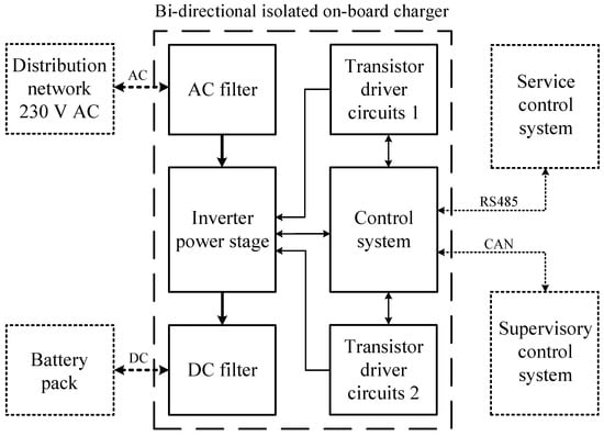
Figure 23.
Block diagram of main modules of bidirectional isolated on-board charger. Each block represents one printed circuit board.

Table 1.
Major parameters of the bidirectional on-board charger.
Inverter power stage contains four power transistors Q1 to Q4 type IPW60R017C7XKSA1, see bridge “A” in Figure 5 and five power transistors Q5 to Q8 and Q13 type C3M0032120K, see bridge “B” and active element “D”, four power transistors Q9 to Q12 type C3M0030090K, see bridge “C” in Figure 5.
For id and iBAT measurements, galvanically isolated current sensors ACS730-KLCTR-50AB-T are used, for ug, ud and uBAT measurements, precision optically isolated voltage sensors ACPL-C87A-500E are used. Capacitors C1, C2 and C13 are able to provide high peak current and are durable and as small as possible. Therefore, they were assembled as a combination of ceramic and foil capacitors.
C1: 7 × 0.33 μF/630 V foil + 7 × 100 nF/1.5 kV X7R ceramic.
C2: 11 × 1 μF/630 V foil + 11 × 100 nF/1.5 kV X7R ceramic.
C13: 4 × 33 nF/1kV + 6 × 22 nF/1kV special pulse ceramic.
Transistor driver circuit 1 contains six drivers of ADUM4135BRWZ type for transistors Q3, Q4, Q6, Q8, Q10 and Q12 and five pieces of galvanically isolated DC/DC power supplies.
Transistor driver circuit 2 contains seven drivers of ADUM4135BRWZ type for transistors Q1, Q2, Q5, Q7, Q9, Q11 and Q13 and seven pieces of galvanically isolated DC/DC power supplies.
Control system contains five galvanically isolated power supplies, linear regulators (5, 3.3 V), 3.3 V voltage reference for AD converter and analogue supply for microcontroller, circuit for isolated measurement of voltages and currents, two high-speed CAN transceivers, service communication interface with RS485, temperature measurement and 32-bit microcontroller ARM Cortex M4, STM32F446XC (STMicroelectronics, Geneva, Switzerland).
Microcontroller STM32F446XC works at 180 MHz system clock, and five timers are used to control charging and discharging mode. For every single transistor control, specific timer output was assigned. For example, channel 1 of timer TIM1 for transistor pair Q5, Q8. All timers utilise asymmetric PWM. To better understand the control algorithms, logic signals for charging mode are shown in Figure 9 and in Figure 15 for discharging mode. Duration labelled as tdelay is in charging mode realised with phase shift of timers. In discharging mode the duration tdelay for transistors Q5 to Q8 is realised with timer dead time and for transistor Q13 with phase shift of timer.
Considering the requirements for as small as possible dimensions and weight, fluid cooling was selected for transistor cooling. The simulation focused on thermal transfer, and fluid movement in the heatsink was performed in software COMSOL Multiphysics 5.5 (COMSOL Inc., Stockholm, Sweden). For both charging and discharging modes, the temperature 80 °C without radiation effects was assumed. All the heat is dissipated through the heatsink. This simplification corresponds to real conditions in the charger, whose internal space is heated-up with power dissipation of the remaining components. To prevent overheating damage of power transistors, simulations of the maximal possible temperature of cooling fluid were performed. It showed that it is possible to reach up to 110 °C of cooling fluid without exceeding the absolute maximum temperature rating of the transistor junction.
Two variants of transistor Q1 to Q13 control techniques were simulated in charging and discharging modes.
In the first variant, referred to as “Uncontrolled”, only transistors Q5 to Q8 and Q13 were driven in charging mode and only transistors Q1 to Q4, Q9 to Q12 and Q13 were driven in discharging mode. In the second variant, referred to as “Controlled”, all transistors were actively driven.
The inlet temperature of the coolant is 80 °C at a flow rate of 2 L/min.
Figure 24 shows the example of temperature simulation of all transistors placed on the heatsink. This is for maximal power of the charger and active control of all transistors in charging mode. Coolant inlet temperature was 80 °C, and outlet temperature was 82.2 °C at a flow rate of 2 L/min.
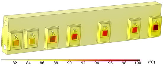
Figure 24.
Transistor temperatures in charging mode and active control of all transistors. Left to right: Q1, Q2, Q13, Q5, Q7, Q11 a Q9.
Figure 25 shows a photograph of the new prototype of the bidirectional charger enhanced with an active element “D”. Dimensions: 224 × 100 × 130 mm (W × D × H).
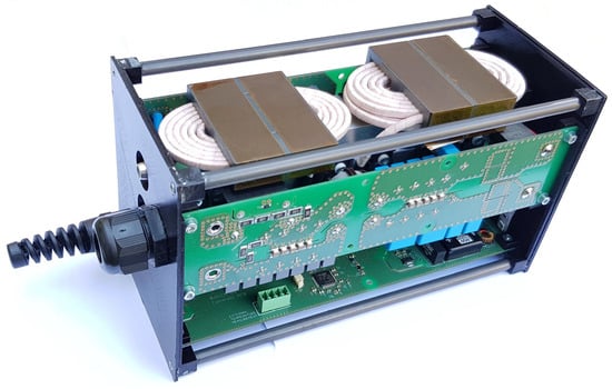
Figure 25.
A photograph of the second prototype of the bidirectional isolated on-board charger.
5. The Experimental Microgrid Platform
The experimental microgrid platform for the development of the Vehicle to Grid technologies simulates the electricity consumption of a typical single-family home. The microgrid system is based on a hybrid AC/DC architecture. The centre of the experimental platform is a Conext XW+ 8548 E hybrid inverter (Schneider Electric SE, Rueil-Malmaison, France). The testing platform consists of two parts. The first part is based on the main 48 V DC bus, whereas the second is based on the 230 V AC bus. The DC part consists of two Conext 80 600 DC/DC-MPPT PV inverters (Schneider Electric SE, Rueil-Malmaison, France). These PV inverters convert electricity to supply appliances and storage batteries from photovoltaic strings. The batteries are thin plate pure lead Hawker 12XFC115. One battery’s nominal voltage and capacity are 12 V and 115 Ah. These batteries are connected in a battery bank, forming four groups, each including four batteries. The 48 V DC bus voltage varies from 40.5 to 64 V DC depending on the battery’s state of charge and the charging process. The rated power of each of the two PV strings is 2 kW. The second part of the platform is based on a 230 V AC bus with a frequency of 50 Hz. The AC bus is drawn directly from the hybrid inverter to which the individual household appliances are connected. Figure 26 shows a schematic of the microgrid system used to perform the experiments in this article.
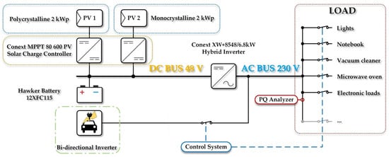
Figure 26.
Diagram of the entire test platform.
Every part of testing platform communicates between self. The authors’ previous work in the field of power-line communication (PLC) technology describes potential concepts of the real-time communication in off-grid electrical systems [40].
6. Results and Discussion
For experimental verification of the bidirectional charger, a new prototype enhanced with an active element “D” was assembled, and a new control strategy of transistors Q9 to Q12 was used. The measurement station mainly consisted of the following instruments: Rigol MSO4054 oscilloscope, Micsig DP 10013 high voltage differential probe, Rigol RP1002C current probe, PEM CWTUM/03/B ultra-miniature HF current probe.
In Section 2.2, waveforms of voltages and currents in charging mode with inductor inductance 25 μH were shown. Those waveforms were acquired while using the new topology according to Figure 1, i.e., without active element “D”. Figure 27 shows waveforms of voltages and currents in charging mode with the topology according to Figure 5, i.e., with the active element “D”. Comparing Figure 4 and Figure 27, it is obvious that up and uab overvoltage problem, caused by transformer leakage inductance, was solved by the active element “D”. Voltage up waveform after modification contains higher frequency oscillations caused by other parasitic properties, which were not present with the topology according to Figure 1. The root cause of these oscillations is mainly the parasitic properties of PCBs and electronic components. These oscillations have much lower amplitude and do not overstress the semiconductors with overvoltage. Voltage up amplitude is, in this case, equal to 600 V and did not exceed the absolute maximum voltage of 700 V, see Section 3.1. Dumped resonances of voltage us (Figure 4), caused by circuit parasitic on the secondary side of the transformer, were successfully suppressed with alternative control strategy of transistors Q9 to Q12, different to what was mentioned in Section 2.1.
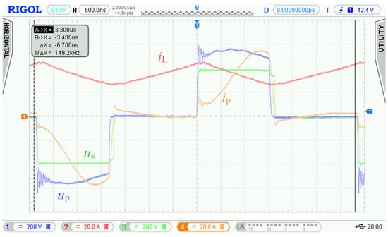
Figure 27.
Experimental measurement in charging mode with active element “D”. Measured at: ug = 240.3 V, ig = 33.5 A, pg = 8049.9 W, uBAT = 371.1 V, iBAT = 20.5 A, fs = 150 kHz. Channel description: 1 = up, 2 = iL, 3 = us, 4 = ip.
6.1. Experimental Measurement Results Acquired in Charging Mode
Figure 27 shows waveforms of the different quantities during single switching period. Measurement was taken at nominal power and represented its specific time instant.
Figure 28 shows the voltage and current waveforms over a time interval of several periods of the 50 Hz power grid at rated power. The figure implies that waveforms of power grid current ig follow the shape of power grid voltage ug with minimal total harmonic distortions and phase shift (unity power factor).
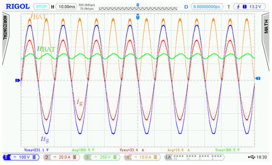
Figure 28.
Experimental waveforms of voltages and currents measured in charging mode of bidirectional charger connected to 230 V AC power grid. Requested battery current IBATr = 20 A. Measured values: Ug = 231.1 V, Ig = 33.4 A, UBAT = 366.5 V, IBAT = 19.6 A. Channel description: 1 = ug, 2 = ig, 3 = uBAT, 4 = iBAT.
Distortion of battery current iBAT was caused by dynamic properties of the used electronic artificial load connected to the battery. This electronic load substituted insufficient battery capacity as well as dissipated energy during charging mode. This prevented repetitive battery cycling during the experimental measurements.
The control principle supports very high dynamics of change of power grid current ig, but its dynamics is reduced with respect to requirements and usage of the bidirectional charger.
6.2. Experimental Measurement Results Acquired in Discharging Mode
Figure 29 shows the voltage and current waveforms during one single switching period. It shows the values corresponding to a specific time interval at rated power.
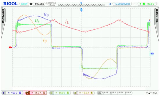
Figure 29.
Experimental measurement in discharging mode with active element “D”. Measured at: ton = 1.79 μs, tQ13 = 1.71 μs, tdelay = 0.08 μs, ug = 229.1 V, ig = 31.2 A, pg = 7147.9 W, uBAT = 330.4 V, iBAT = 22.6 A, fs = 150 kHz. Channel description: 1 = up, 2 = iL, 3 = us, 4 = ip.
Figure 30 shows the voltage and current waveforms over a time interval of three periods of the 50 Hz power grid. The waveforms also indicate minimal harmonic distortion, similarly to the charging mode.
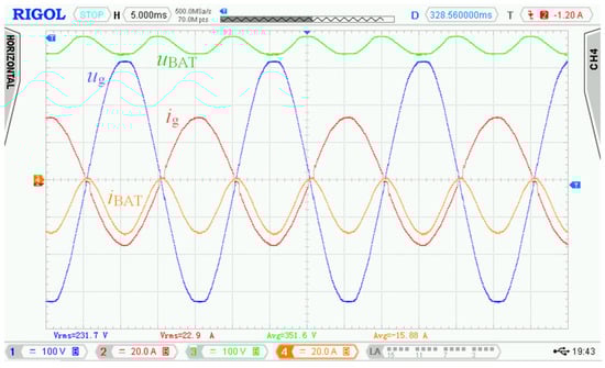
Figure 30.
Experimental waveforms of voltages and currents in discharging mode and bidirectional charger connected to power grid 230 V AC. Requested battery current IBATr = 15 A (3 periods of power grid). Measured values: Ug = 231.7 V, Ig = 22.9 A, UBAT = 351.6 V, IBAT = 15.9 A. Channel description: 1 = ug, 2 = ig, 3 = uBAT, 4 = iBAT.
Optimal function and maximum efficiency in charging and discharging mode is achieved with active control of all transistors Q1 to Q13.
Figure 31 shows the efficiency curve of the bidirectional charger for battery voltages of 300 and 400 V. The maximum efficiency of the bidirectional charger in charging mode for a battery voltage of 300 V was 96.4% at 3.4 kW and for a battery voltage of 400 V was 95.6% at 4.6 kW. The maximum efficiency in discharge mode for 300 V battery was 96.3% at 3.8 kW and for 400 V battery, voltage was 95.7% at 4.4 kW, see Figure 31.
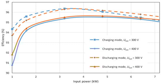
Figure 31.
Measured efficiency of the bidirectional galvanically isolated on-board charger.
The following EMC measurements were carried out on the new prototype of the bidirectional charger:
Conducted Emissions Tests (CE)
- CE02—Conducted Emission, Voltage method (IEC CISPR 25)
Radiated Emissions Tests (RE)
- RE01, Radiated Emission, ALSE method (IEC CISPR 25)
Immunity to ElectroStatic Discharges Tests (ESD)
- ESD02, Unpowered test (ISO 10605)
- TP01, Immunity to transient pulse 1 and 1b (ISO 7637-2)
- TP02, Immunity to transient pulse 2 (ISO 7637-2)
- TP03, Immunity to transient pulse 3a and 3b (ISO 7637-2)
- TP04, Immunity to transient pulse 4 (ISO 7637-2)
- TP05, Immunity to transient pulse 5 (ISO 7637-2)
The results of all these EMC measurements meet the given criteria.
Figure 32 shows the emissions testing waveform for the bidirectional charger.
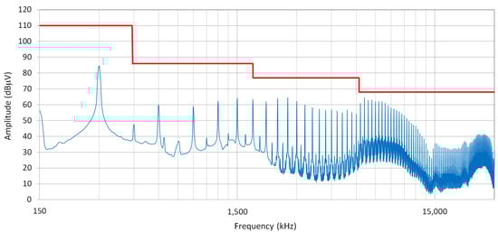
Figure 32.
Conducted emissions testing. Voltage method according to CISPR 25. Ug = 230 V, Ig = 15 A.
7. Conclusions
This paper describes the research, development and experimental testing of a bidirectional galvanically isolated on-board charger for electric vehicles. The main objective was to meet the requirements of 4 kW/kg and 2 kW/dm3, bidirectional power control and galvanic insulation from the power grid. The power density of the realised charger was 4 kW/kg and 2.46 kW/dm3, and the maximum efficiency was 96.4% at 3.4 kW. To be able to achieve such low weight and values, specific electronic and mechanical elements had to be addressed. As for the electronic circuits, we mostly addressed the inductor and transformer, and as for the mechanical components, the solution concerned the heatsink. To achieve as low weight and volume as possible, fluid cooling was used to cool down the power transistors. To make the inductor and transformer smaller, high switching frequency of 150 kHz had to be used.
Based on the state-of-the-art research, a circuit scheme of the bidirectional charger was proposed, and a prototype for testing the control algorithms was built. In fact, several prototypes were built, two most prominent being described in this paper. The first prototype of the charger is described in Section 2, where problems and their solutions are also dealt with. Due to the parasitic properties of the transformer and other electronic circuits, overvoltage and oscillations occurred across the primary winding of the transformer. There was also dumped resonance across the secondary winding. Those undesirable effects were eliminated with topology modification by adding an active element “D” into the charger and with new Q9 to Q13 control strategy. The feasibility of this solution was verified with a new prototype of the bidirectional charger, which is described in Section 4. The novel switching strategy of Q9 to Q13 transistors’ control and modified topology with an active element “D” were patented. The realised charger has an output of either 7.2 kW if it uses only single-phase or 21.6 kW if it uses three-phases.
The contribution of this work can be summarised as follows:
- The single-stage inverter topology was modified to eliminate undesirable phenomena.
- Bidirectional power control and galvanic insulation from the power grid.
- Owing to the novel switching strategy of Q9 to Q12 transistors’ control, the charger does not need RCD snubbers in order to limit the voltage spikes caused by leakage inductance of the transformer. This has the effect of reducing losses, increasing efficiency and also reducing weight and volume.
- The proposed transistor switching control method eliminates unwanted HF oscillations on both the primary and secondary sides of the transformer in the on-board charger.
- In order to reduce the size and weight of the inductor and transformer, high switching frequency of 150 kHz was used.
- The charger allows V2G technology.
- The power density of the new charger was 4 kW/kg and 2.46 kW/dm3, and the maximum efficiency was 96.4% at 3.4 kW.
- The new charger has an output of either 7.2 kW if it uses only single-phase, or 21.6 kW if it uses three-phases.
8. Patents
The solution presented in the paper has been patented. The name of the patent is “Charger for bidirectional energy flow and controlling it”. The patent number is PUV 2020-37617 (308969), CZ2020236A3.
Author Contributions
Conceptualisation, R.H., V.K. and L.H.; methodology, R.H. and L.H.; software, R.H.; validation, R.H., L.H. and V.B.; formal analysis, T.V.; investigation, T.V.; resources, S.M.; data curation, R.H.; writing—original draft preparation, R.H., V.K., V.B. and M.B.; writing—review and editing, R.H., V.B. and M.B.; visualisation, R.H.; supervision, S.M.; project administration, Z.S.; funding acquisition, Z.S. All authors have read and agreed to the published version of the manuscript.
Funding
This work was supported by the Doctoral grant competition VSB—Technical University of Ostrava, reg. no. CZ.02.2.69/0.0/0.0/19_073/0016945 within the Operational Programme Research, Development and Education, under project DGS/TEAM/2020-017 “Smart Control System for Energy Flow Optimization and Management in a Microgrid with V2H/V2G Technology” and SP2022/17 “Research in the field of intelligent building control, asynchronous motors in fault conditions, feedback effects of controlled drives, measurement of ground current fields and biological effects”.
Institutional Review Board Statement
Not applicable.
Informed Consent Statement
Not applicable.
Data Availability Statement
Not applicable.
Conflicts of Interest
The authors declare no conflict of interest.
Patent Annotation
Charger for bidirectional energy flow, which has on the way from the mains voltage source (ug) to the battery: the first bidirectional converter (A) consisting of switches (S1 to S4) operating on the mains frequency, the second bidirectional converter (B) consisting of switches (S5 to S8) operating at a frequency in the order of hundreds of kHz, a transformer (TR) and a third bidirectional converter (C) consisting of switches (S9 to S12) operating at the same frequency as the second converter. A coil (L) is connected in one of the buses (+, −) connecting the first and second converters (B, C), behind which the buses (+, −) are connected via a separate switch (S13) and a capacitor (C13). The method of controlling the charger by the control unit for the mains battery charging phase consists of a signal from the control unit being switched by a switch (S13) with period T/2 and the second and third converters (B, C) are switched with period T. For safety reasons, the control unit leaves the switch (S13) open for additional time during the safety delays tdead and tdelay before the interval t0, or after this interval t0.
References
- Globisch, J.; Plötz, P.; Dütschke, E.; Wietschel, M. Consumer Evaluation of Public Charging Infrastructure for Electric Vehicles; Working Paper Sustainability and Innovation; No. S13/2018; Fraunhofer-Institut für System- und Innovationsforschung ISI: Karlsruhe, Germany, 2018. [Google Scholar]
- Miller, I.; Arbabzadeh, M.; Gençer, E. Hourly Power Grid Variations, Electric Vehicle Charging Patterns, and Operating Emissions. Environ. Sci. Technol. 2020, 54, 16071–16085. [Google Scholar] [CrossRef]
- Elghitani, F.; El-Saadany, E.F. Efficient Assignment of Electric Vehicles to Charging Stations. IEEE Trans. Smart Grid 2021, 12, 761–773. [Google Scholar] [CrossRef]
- Mohammed, S.A.Q.; Jung, J.-W. A Comprehensive State-of-the-Art Review of Wired/Wireless Charging Technologies for Battery Electric Vehicles: Classification/Common Topologies/Future Research Issues. IEEE Access 2021, 9, 19572–19585. [Google Scholar] [CrossRef]
- Hee, C.S. An Electric Vehichle Charger Having Load Smoothing Function. Korean Patent KR20120086388A, 3 August 2012. [Google Scholar]
- Nezamuddin, O.N.; Nicholas, C.L.; Santos, E.C. dos The Problem of Electric Vehicle Charging: State-of-the-Art and an Innovative Solution. IEEE Trans. Intell. Transp. Syst. 2022, 23, 4663–4673. [Google Scholar] [CrossRef]
- Jafari, M.; Kavousi-Fard, A.; Niknam, T.; Avatefipour, O. Stochastic Synergies of Urban Transportation System and Smart Grid in Smart Cities Considering V2G and V2S Concepts. Energy 2021, 215, 119054. [Google Scholar] [CrossRef]
- CEN-CENELEC-ETSI Smart Grid Coordination Group CEN-CENELEC-ETSI Smart Grid Coordination Group Smart Grid Reference Architecture. CENELEC. 2012. Available online: https://www.cencenelec.eu/media/CEN-CENELEC/AreasOfWork/CEN-CENELEC_Topics/Smart%20Grids%20and%20Meters/Smart%20Grids/reference_architecture_smartgrids.pdf (accessed on 26 October 2022).
- Shabanzadeh, M.; Moghaddam, M. What Is the Smart Grid? Definitions, Perspectives, and Ultimate Goals. In Proceedings of the Power System Conference, September 28th International Power System Conference (PSC), Tehran, Iran, 13 November 2013. [Google Scholar]
- Fernandez-Jimenez, L.A.; Muñoz-Jimenez, A.; Falces, A.; Mendoza-Villena, M.; Garcia-Garrido, E.; Lara-Santillan, P.M.; Zorzano-Alba, E.; Zorzano-Santamaria, P.J. Short-Term Power Forecasting System for Photovoltaic Plants. Renew. Energy 2012, 44, 311–317. [Google Scholar] [CrossRef]
- Shaqsi, A.Z.A.L.; Sopian, K.; Al-Hinai, A. Review of Energy Storage Services, Applications, Limitations, and Benefits. Energy Rep. 2020, 6, 288–306. [Google Scholar] [CrossRef]
- Verma, A.; Singh, B.; Chandra, A.; Al-Haddad, K. An Implementation of Solar PV Array Based Multifunctional EV Charger. In Proceedings of the 2018 IEEE Transportation Electrification Conference and Expo (ITEC), Long Beach, CA, USA, 13–15 June 2018; pp. 531–536. [Google Scholar]
- Berthold, F.; Ravey, A.; Blunier, B.; Bouquain, D.; Williamson, S.; Miraoui, A. Design and Development of a Smart Control Strategy for Plug-In Hybrid Vehicles Including Vehicle-to-Home Functionality. IEEE Trans. Transp. Electrif. 2015, 1, 168–177. [Google Scholar] [CrossRef]
- Çelik, D.; Meral, M.E. A Coordinated Virtual Impedance Control Scheme for Three Phase Four Leg Inverters of Electric Vehicle to Grid (V2G). Energy 2022, 246, 123354. [Google Scholar] [CrossRef]
- Wickramasinghe Abeywardana, D.B.; Acuna, P.; Hredzak, B.; Aguilera, R.P.; Agelidis, V.G. Single-Phase Boost Inverter-Based Electric Vehicle Charger with Integrated Vehicle to Grid Reactive Power Compensation. IEEE Trans. Power Electron. 2018, 33, 3462–3471. [Google Scholar] [CrossRef]
- Zhang, H.; Hu, Z.; Xu, Z.; Song, Y. Evaluation of Achievable Vehicle-to-Grid Capacity Using Aggregate PEV Model. IEEE Trans. Power Syst. 2017, 32, 784–794. [Google Scholar] [CrossRef]
- Jawad, M.; Qureshi, M.B.; Ali, S.M.; Shabbir, N.; Khan, M.U.S.; Aloraini, A.; Nawaz, R. A Cost-Effective Electric Vehicle Intelligent Charge Scheduling Method for Commercial Smart Parking Lots Using a Simplified Convex Relaxation Technique. Sensors 2020, 20, 4842. [Google Scholar] [CrossRef]
- Schlüter, J.; Weyer, J. Car Sharing as a Means to Raise Acceptance of Electric Vehicles: An Empirical Study on Regime Change in Automobility. Transp. Res. Part F Traffic Psychol. Behav. 2019, 60, 185–201. [Google Scholar] [CrossRef]
- Jung, J.; Koo, Y. Analyzing the Effects of Car Sharing Services on the Reduction of Greenhouse Gas (GHG) Emissions. Sustainability 2018, 10, 539. [Google Scholar] [CrossRef]
- Sam, C.A.; Jegathesan, V. Bidirectional Integrated On-Board Chargers for Electric Vehicles—A Review. Sādhanā 2021, 46, 26. [Google Scholar] [CrossRef]
- Whitaker, B.; Barkley, A.; Cole, Z.; Passmore, B.; Martin, D.; McNutt, T.R.; Lostetter, A.B.; Lee, J.S.; Shiozaki, K. A High-Density, High-Efficiency, Isolated On-Board Vehicle Battery Charger Utilizing Silicon Carbide Power Devices. IEEE Trans. Power Electron. 2014, 29, 2606–2617. [Google Scholar] [CrossRef]
- Beniak, R.; Górecki, K.; Paduch, P.; Rogowski, K. Reduced Switch Count in Space Vector PWM for Three-Level NPC Inverter. Energies 2020, 13, 5945. [Google Scholar] [CrossRef]
- Neborak, I.; Sladecek, V.; Kuchar, M. Modelling and Simulation of Induction Machine and Frequency Converter Considering Power Losses. In Proceedings of the 2015 16th International Scientific Conference on Electric Power Engineering (EPE), Ostrava, Czech Republic, 20–22 May 2015; pp. 251–255. [Google Scholar]
- Gowda, C.K.; Khedekar, V.G.; Anandh, N.; Paragond, L.R.S.; Kulkarni, P. Bidirectional On-Board EV Battery Charger with V2H Application. In Proceedings of the 2019 Innovations in Power and Advanced Computing Technologies (i-PACT), Vellore, India, 22–23 March 2019; pp. 1–5. [Google Scholar]
- Nassary, M.; Orabi, M.; Ghoneima, M.; El-Nemr, M.K. Single-Phase Isolated Bidirectional AC-DC Battery Charger for Electric Vehicle—Review. In Proceedings of the 2019 International Conference on Innovative Trends in Computer Engineering (ITCE), Aswan, Egypt, 2–4 February 2019; pp. 581–586. [Google Scholar]
- Karthikeyan, V.; Gupta, R. Light-Load Efficiency Improvement by Extending ZVS Range in DAB-Bidirectional DC-DC Converter for Energy Storage Applications. Energy 2017, 130, 15–21. [Google Scholar] [CrossRef]
- De Doncker, R.W.A.A.; Divan, D.M.; Kheraluwala, M.H. A Three-Phase Soft-Switched High-Power-Density DC/DC Converter for High-Power Applications. IEEE Trans. Ind. Appl. 1991, 27, 63–73. [Google Scholar] [CrossRef]
- Jauch, F.; Biela, J. Single-Phase Single-Stage Bidirectional Isolated ZVS AC-DC Converter with PFC. In Proceedings of the 2012 15th International Power Electronics and Motion Control Conference (EPE/PEMC), Novi Sad, Serbia, 4–6 September 2012; pp. LS5d.1-1–LS5d.1-8. [Google Scholar]
- Ramli, M.Z.; Salam, Z.; Toh, L.S.; Nge, C.L. A Bidirectional High-Frequency Link Inverter Using Center-Tapped Transformer. In Proceedings of the 2004 IEEE 35th Annual Power Electronics Specialists Conference (IEEE Cat. No.04CH37551), Aachen, Germany, 20–25 June 2004; pp. 3883–3888. [Google Scholar]
- Everts, J.; Krismer, F.; van den Keybus, J.; Driesen, J.; Kolar, J.W. Optimal ZVS Modulation of Single-Phase Single-Stage Bidirectional DAB AC–DC Converters. IEEE Trans. Power Electron. 2014, 29, 3954–3970. [Google Scholar] [CrossRef]
- Ostlund, S. Reduction of Transformer Rated Power and Line Current Harmonics in a Primary Switched Converter System for Traction Applications. In Proceedings of the 1993 Fifth European Conference on Power Electronics and Applications, Brighton, UK, 13–16 September 1993; Volume 7, pp. 112–119. [Google Scholar]
- Norrga, S. A Soft-Switched Bi-Directional Isolated AC/DC Converter for AC-Fed Railway Propulsion Applications. In Proceedings of the International Conference on Power Electronics Machines and Drives, Bath, UK, 16–18 April 2002; pp. 433–438. [Google Scholar]
- Jiang, J.; Bao, Y.; Wang, L. Topology of a Bidirectional Converter for Energy Interaction between Electric Vehicles and the Grid. Energies 2014, 7, 4858–4894. [Google Scholar] [CrossRef]
- Kjaer, S.B.; Pedersen, J.K.; Blaabjerg, F. Power Inverter Topologies for Photovoltaic Modules-a Review. In Proceedings of the Conference Record of the 2002 IEEE Industry Applications Conference, 37th IAS Annual Meeting (Cat. No.02CH37344), Pittsburgh, PA, USA, 13–18 October 2002; pp. 782–788. [Google Scholar]
- Shi, F.; Li, R.; Yang, J.; Yu, W. High Efficiency Bidirectional DC-DC Converter with Wide Gain Range for Photovoltaic Energy Storage System Utilization. In Proceedings of the 2018 IEEE International Power Electronics and Application Conference and Exposition (PEAC) 2018, Shenzhen, China, 4–7 November 2018; pp. 1–6. [Google Scholar]
- Liu, Y.-C.; Huang, B.-S.; Lin, C.-H.; Kim, K.A.; Chiu, H.-J. Design and Implementation of a High Power Density Active-Clamped Flyback Converter. In Proceedings of the 2018 International Power Electronics Conference (IPEC-Niigata 2018-ECCE Asia), Niigata, Japan, 20–24 May 2018; pp. 2092–2096. [Google Scholar]
- Ahmed, M.R.; Li, Y. A Low-Cost, High-Power-Density DC-DC Converter for Hybrid and Electric Vehicle Applications. In Proceedings of the 2019 21st European Conference on Power Electronics and Applications (EPE’19 ECCE Europe), Genova, Italy, 3–5 September 2019; pp. P.1–P.8. [Google Scholar]
- Zhu, M.; Shao, C.; Wang, S.; Hang, L.; He, Y.; Fan, S. System Design of Dual Active Bridge (DAB) Converter Based on GaN HEMT Device. In Proceedings of the 2019 22nd International Conference on Electrical Machines and Systems (ICEMS), Harbin, China, 11–14 August 2019; pp. 1–6. [Google Scholar]
- Pittini, R.; Mira, M.C.; Zhang, Z.; Knott, A.; Andersen, M.A.E. Analysis and Comparison Based on Component Stress Factor of Dual Active Bridge and Isolated Full Bridge Boost Converters for Bidirectional Fuel Cells Systems. In Proceedings of the 2014 International Power Electronics and Application Conference and Exposition, Shanghai, China, 5–8 November 2014; pp. 1026–1031. [Google Scholar]
- Blazek, V.; Slanina, Z.; Petruzela, M.; Hrbáč, R.; Vysocký, J.; Prokop, L.; Misak, S.; Walendziuk, W. Error Analysis of Narrowband Power-Line Communication in the Off-Grid Electrical System. Sensors 2022, 22, 2265. [Google Scholar] [CrossRef] [PubMed]
Publisher’s Note: MDPI stays neutral with regard to jurisdictional claims in published maps and institutional affiliations. |
© 2022 by the authors. Licensee MDPI, Basel, Switzerland. This article is an open access article distributed under the terms and conditions of the Creative Commons Attribution (CC BY) license (https://creativecommons.org/licenses/by/4.0/).