
C-Axis Textured, 2–3 μm Thick Al0.75Sc0.25N Films Grown on Chemically Formed TiN/Ti Seeding Layers for MEMS Applications
 ,
,
Abstract
:1. Introduction
2. Materials and Methods
2.1. Deposition of Titanium Films
2.2. Deposition of Al0.75Sc0.25N Thin Films
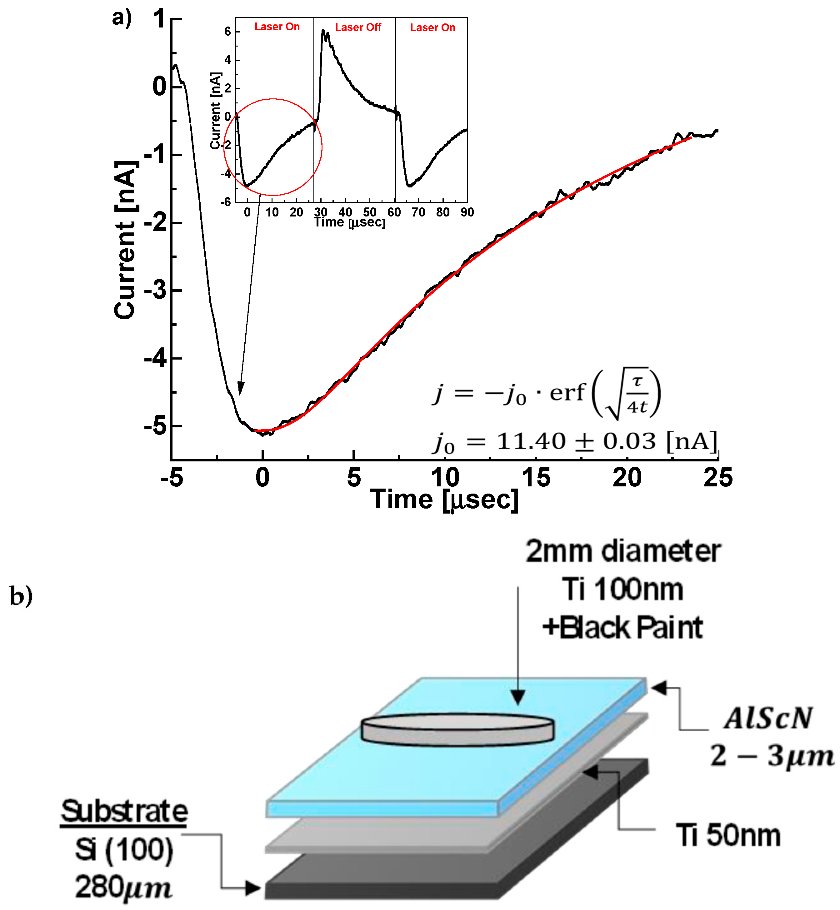
2.3. Measurement of the Piezoelectric Coefficient and Pyroelectric Response
2.4. Film Characterization—SEM, AFM, EDS, XRD, XPS
3. Results
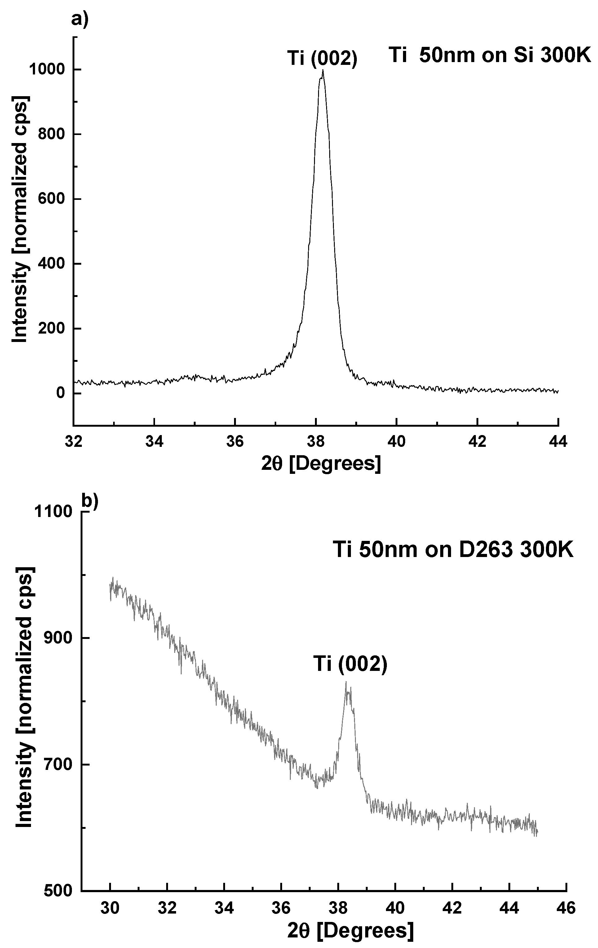
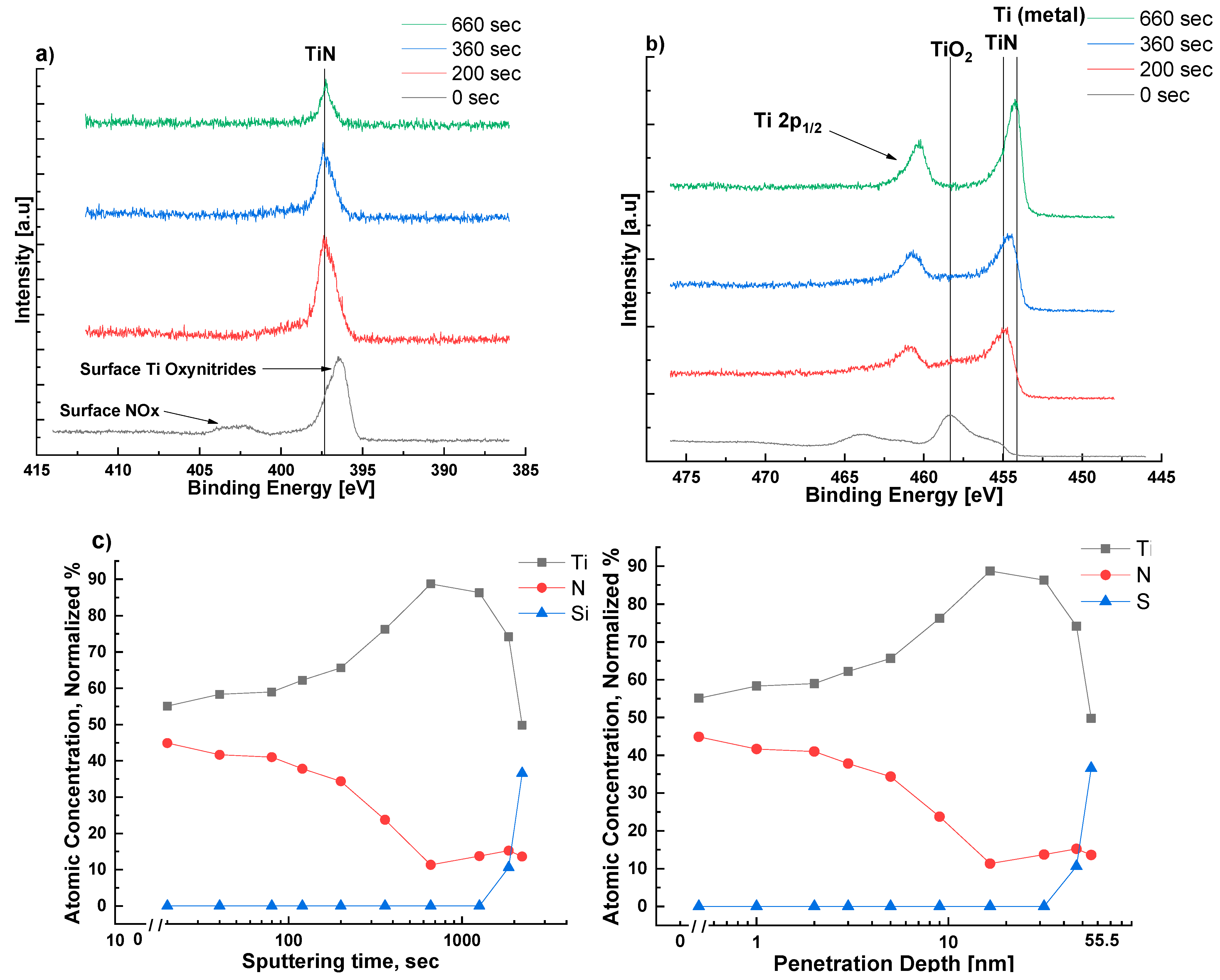
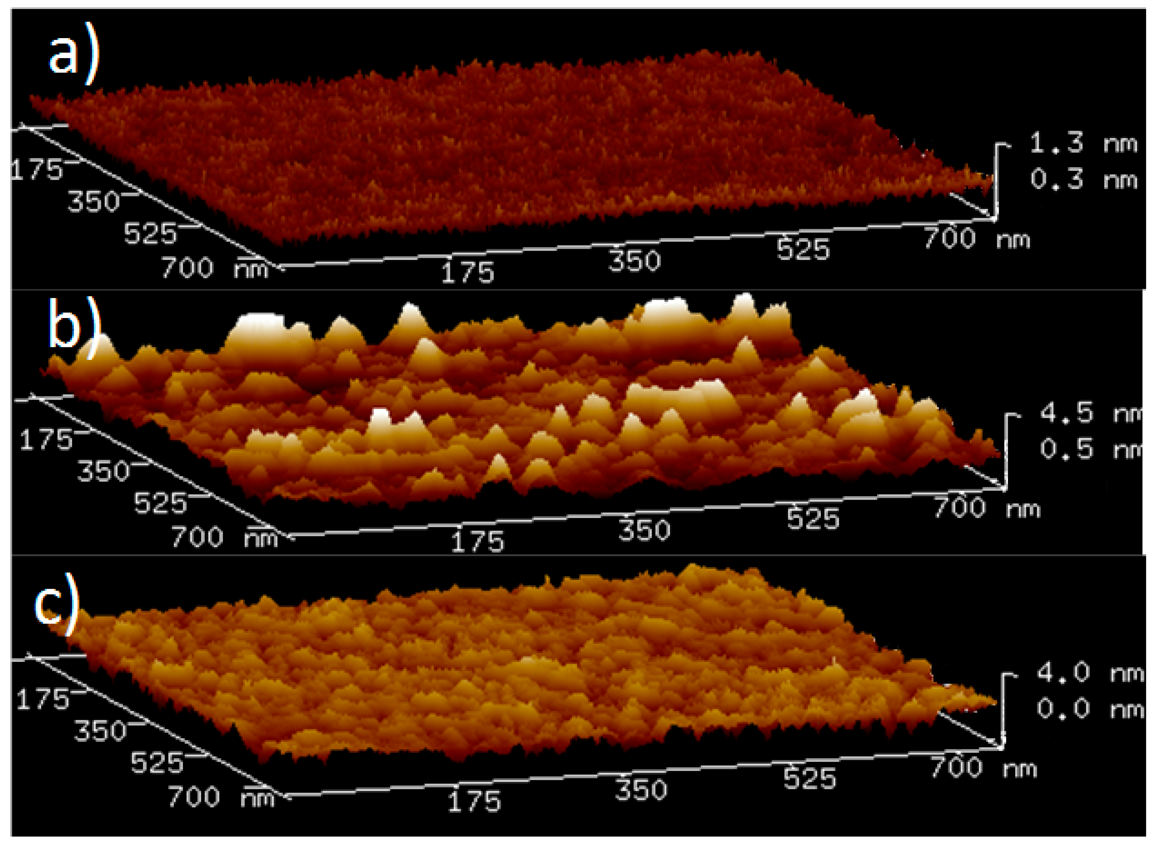
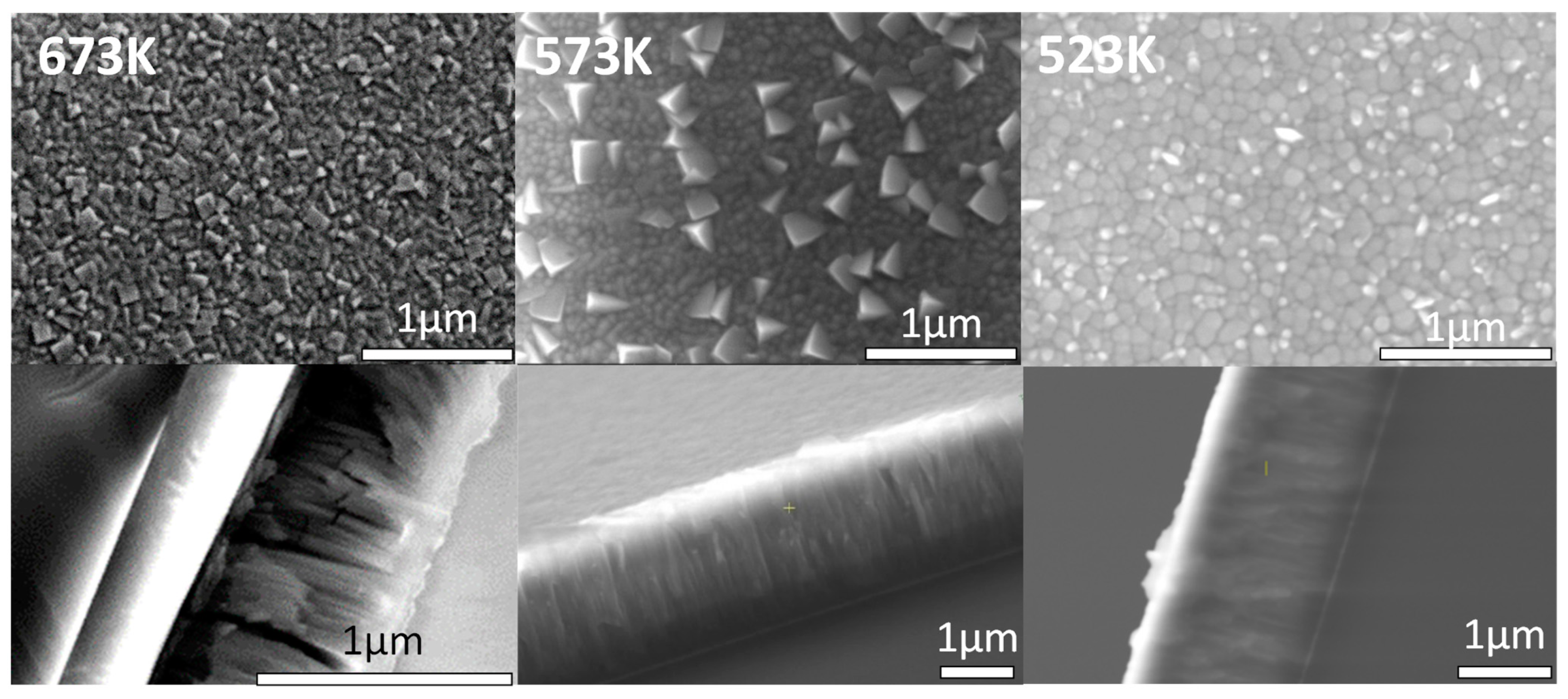
3.1. Formation of TiN on a Ti Seeding Layer
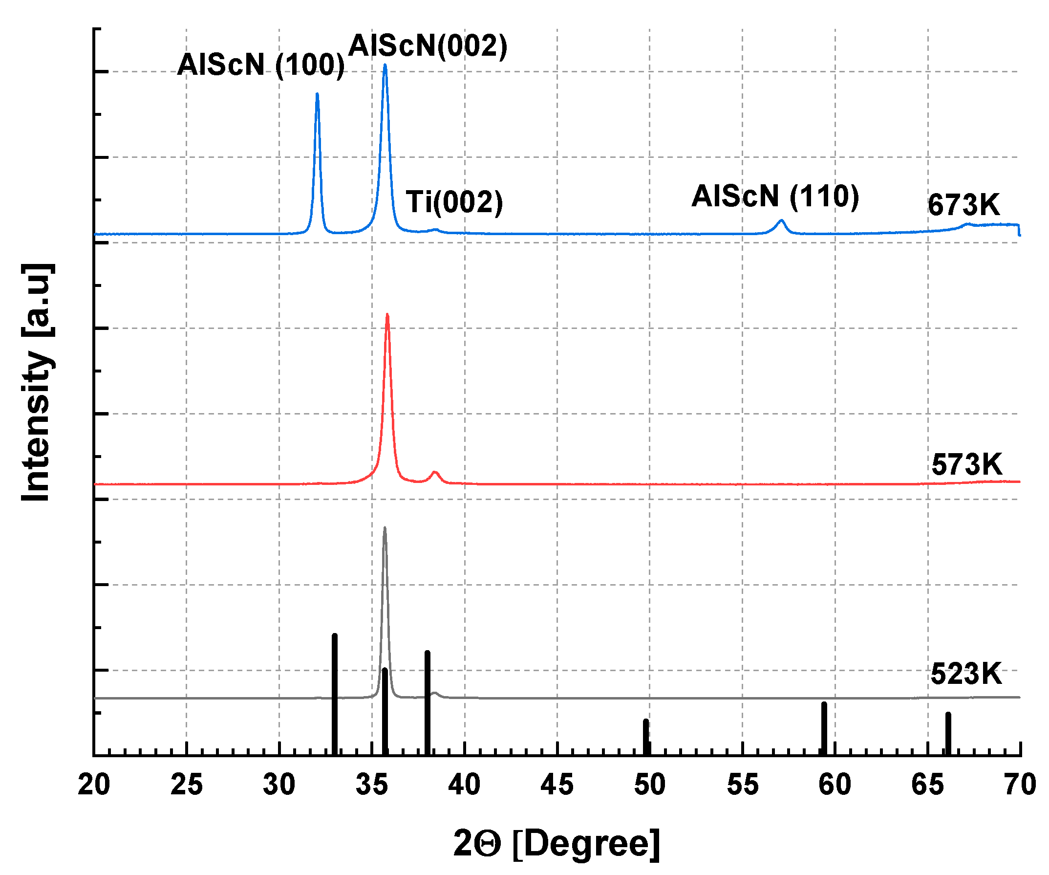
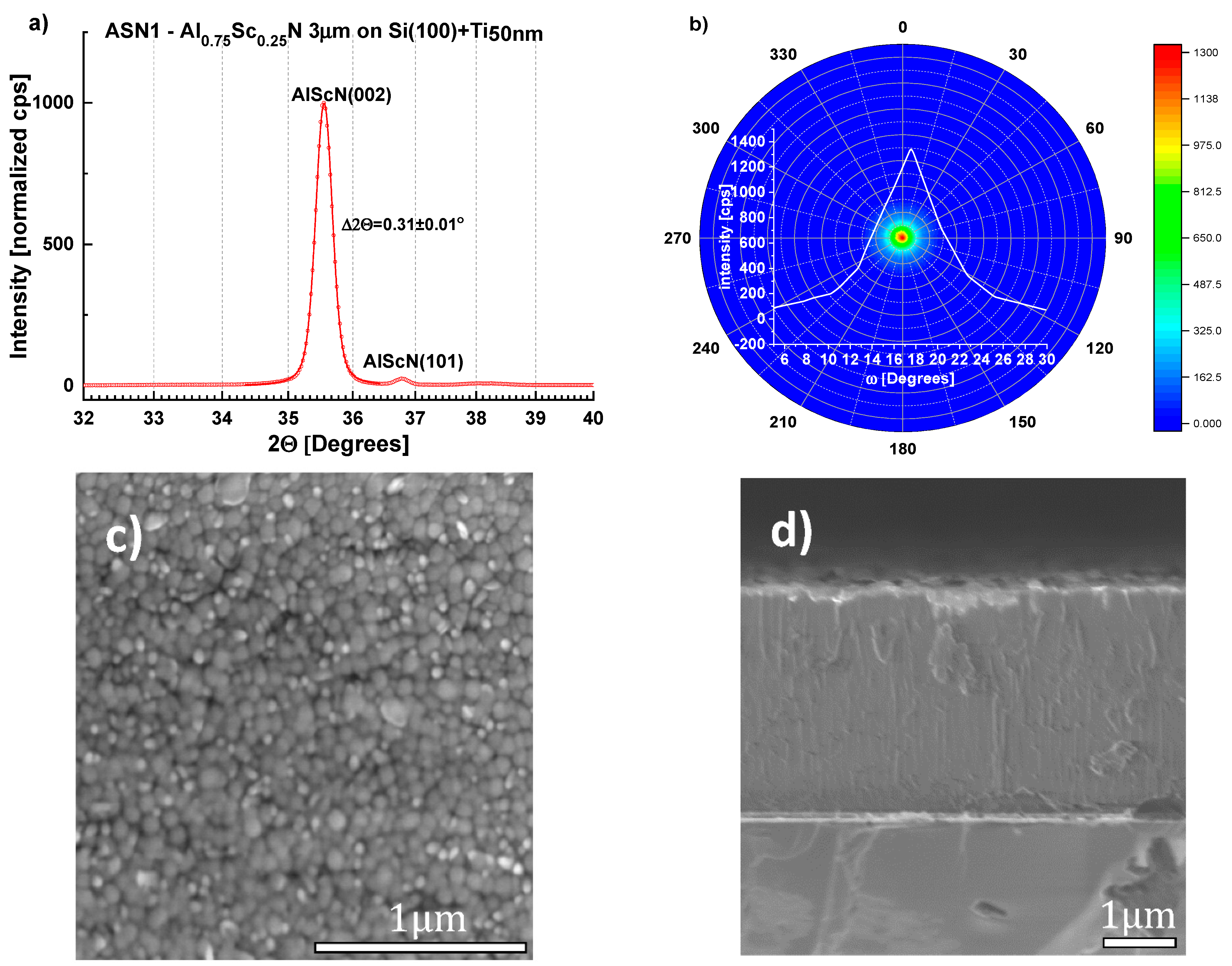
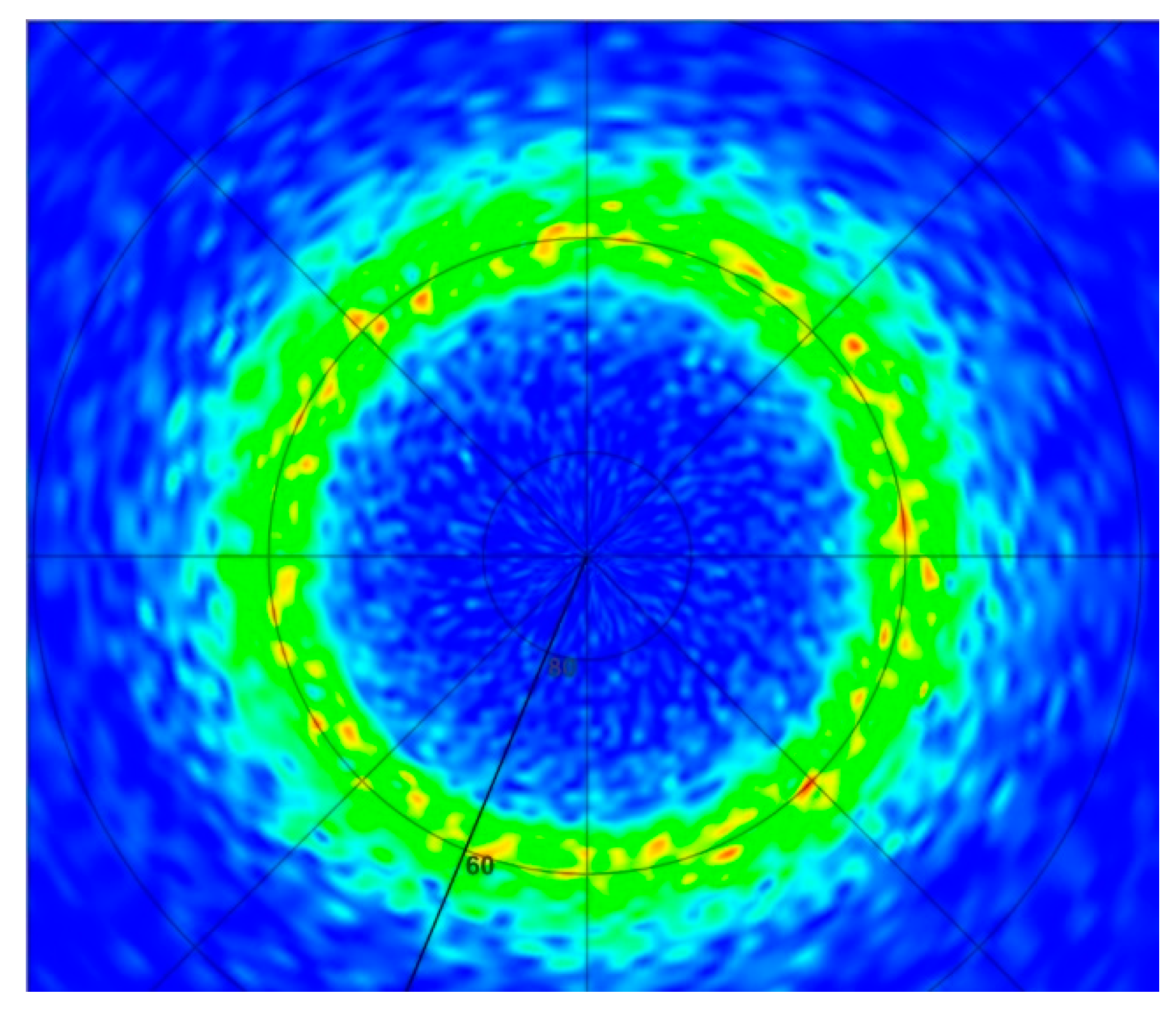
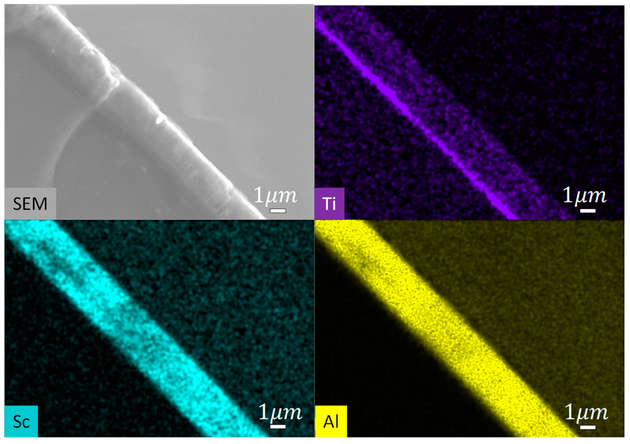
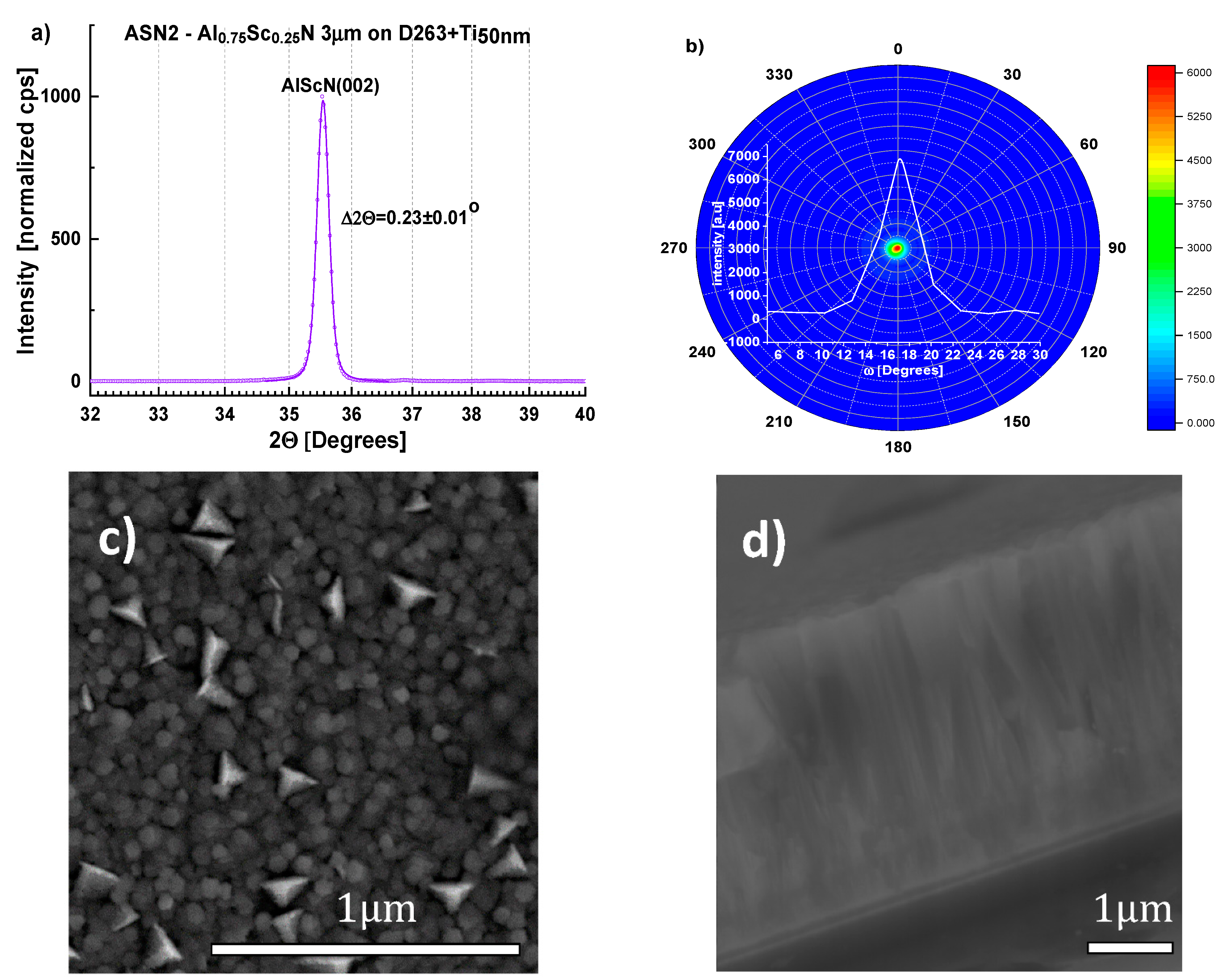
3.2. Reactive Sputtering of AlScN
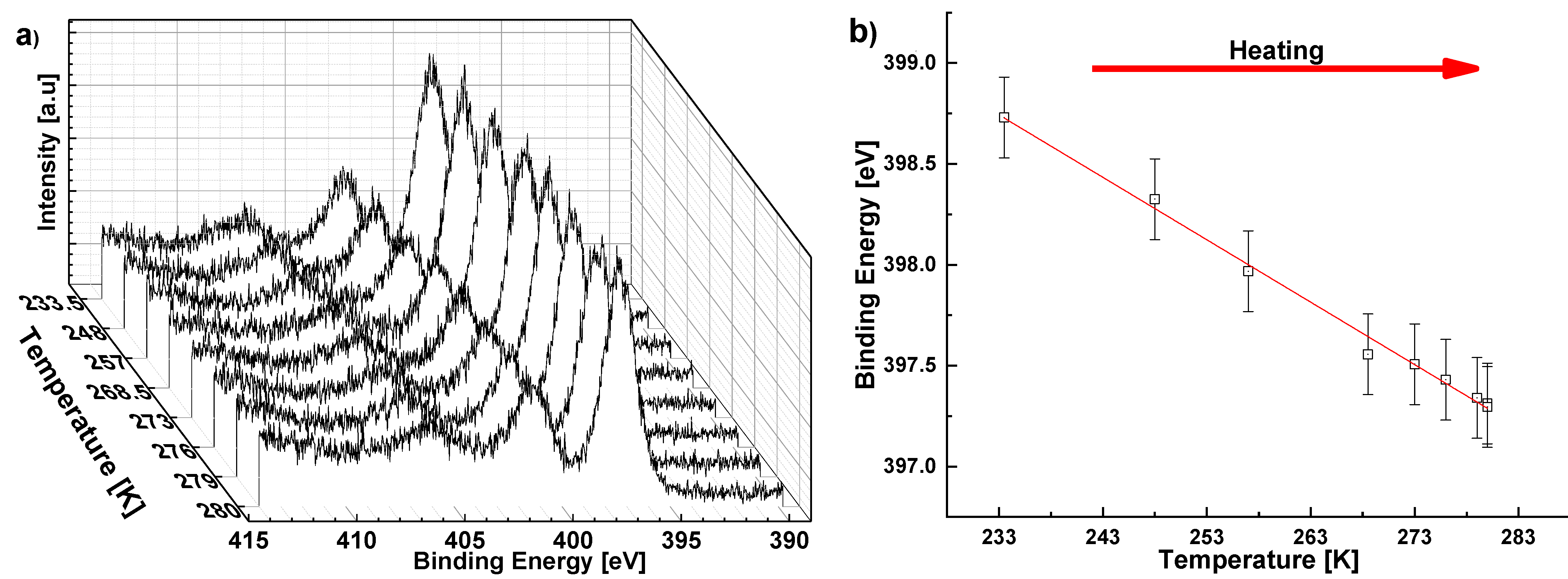
3.3. Pyroelectric Measurements
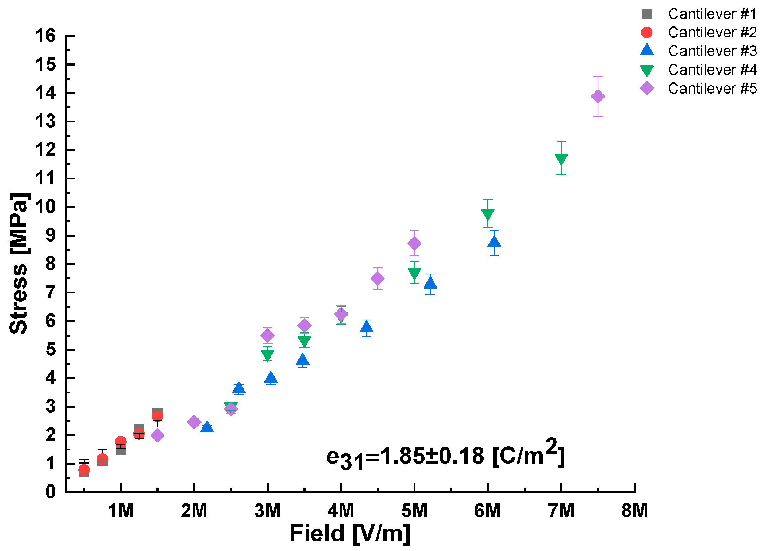
3.4. Measurement of the Piezoelectric Coefficient
4. Summary
5. Patents
Supplementary Materials
Author Contributions
Funding
Institutional Review Board Statement
Informed Consent Statement
Data Availability Statement
Acknowledgments
Conflicts of Interest
References
- Aigner, R.; Kaitila, J.; Ella, J.; Elbrecht, L.; Nessler, W.; Handtmann, M.; Herzog, T.R.; Marksteiner, S. Bulk-Acoustic-Wave Filters: Performance Optimization and Volume Manufacturing. In Proceedings of the IEEE MTT-S International Microwave Symposium Digest, Philadelphia, PA, USA, 8–13 June 2003; Volume 3, pp. 2001–2004. [Google Scholar]
- Elfrink, R.; Kamel, T.M.; Goedbloed, M.; Matova, S.; Hohlfeld, D.; van Andel, Y.; van Schaijk, R. Vibration energy harvesting with aluminum nitride-based piezoelectric devices. J. Micromech. Microeng. 2009, 19, 094005. [Google Scholar] [CrossRef]
- Sandu, C.S.; Parsapour, F.; Mertin, S.; Pashchenko, V.; Matloub, R.; LaGrange, T.; Heinz, B.; Muralt, P. Abnormal Grain Growth in AlScN Thin Films Induced by Complexion Formation at Crystallite Interfaces. Phys. Status Solidi A Appl. Mater. Sci. 2019, 216, 1800569. [Google Scholar] [CrossRef]
- Akiyama, M.; Kano, K.; Teshigahara, A. Influence of growth temperature and scandium concentration on piezoelectric response of scandium aluminum nitride alloy thin films. Appl. Phys. Lett. 2009, 95, 162107. [Google Scholar] [CrossRef]
- Schuster, J.C.; Bauer, J. The Ternary-Systems Sc-Al-N and Y-Al-N. J. Less Common Met. 1985, 109, 345–350. [Google Scholar] [CrossRef]
- Akiyama, M.; Nagao, K.; Ueno, N.; Tateyama, H.; Yamada, T. Influence of metal electrodes on crystal orientation of aluminum nitride thin films. Vacuum 2004, 74, 699–703. [Google Scholar] [CrossRef]
- Iriarte, G.F.; Bjurstrom, J.; Westlinder, J.; Engelmark, F.; Katardjiev, I.V. Synthesis of c-axis-oriented AlN thin films on high-conducting layers: Al, Mo, Ti, TiN, and Ni. IEEE Trans. Ultrason. Ferroelectr. Freq. Control 2005, 52, 1170–1174. [Google Scholar] [CrossRef]
- Mertin, S.; Heinz, B.; Rattunde, O.; Christmann, G.; Dubois, M.A.; Nicolay, S.; Muralt, P. Piezoelectric and structural properties of c-axis textured aluminium scandium nitride thin films up to high scandium content. Surf. Coat. Technol. 2018, 343, 2–6. [Google Scholar] [CrossRef]
- Artieda, A.; Barbieri, M.; Sandu, C.S.; Muralt, P. Effect of substrate roughness on c-oriented AlN thin films. J. Appl. Phys. 2009, 105, 024504. [Google Scholar] [CrossRef]
- Moram, M.A.; Zhang, S. ScGaN and ScAlN: Emerging nitride materials. J. Mater. Chem. A 2014, 2, 6042–6050. [Google Scholar] [CrossRef]
- Esteves, G.; Berg, M.; Wrasman, K.D.; Henry, M.D.; Griffin, B.A.; Douglas, E.A. CMOS compatible metal stacks for suppression of secondary grains in Sc0.125Al0.875N. J. Vac. Sci. Technol. A 2019, 37, 021511. [Google Scholar] [CrossRef]
- Bogner, A.; Timme, H.J.; Bauder, R.; Mutzbauer, A.; Pichler, D.; Krenzer, M.; Reccius, C.; Weigel, R.; Hagelauer, A. Impact of High Sc Content on Crystal Morphology and RF Performance Of Sputtered Al1−xScxN SMR BAW. In Proceedings of the 2019 IEEE International Ultrasonics Symposium (IUS), Glasgow, UK, 6–9 October 2019; pp. 706–709. [Google Scholar]
- Shao, S.; Luo, Z.F.; Wu, T. High Figure-of-Merit Lamb Wave Resonators Based on Al0.7Sc0.3N Thin Film. IEEE Electron Device Lett. 2021, 42, 1378–1381. [Google Scholar] [CrossRef]
- Shao, S.; Luo, Z.F.; Lu, Y.; Mazzalai, A.; Tosi, C.; Wu, T. High Quality Co-Sputtering AlScN Thin Films for Piezoelectric Lamb-Wave Resonators. J. Microelectromech. Syst. 2022, 31, 328–337. [Google Scholar] [CrossRef]
- Beaucejour, R.; Roebisch, V.; Kochhar, A.; Moe, C.G.; Hodge, M.D.; Olsson, R.H. Controlling Residual Stress and Suppression of Anomalous Grains in Aluminum Scandium Nitride Films Grown Directly on Silicon. J. Microelectromech. Syst. 2022, 31, 604–611. [Google Scholar] [CrossRef]
- Rassay, S.; Hakim, F.; Li, C.; Forgey, C.; Choudhary, N.; Tabrizian, R. A Segmented-Target Sputtering Process for Growth of Sub-50 nm Ferroelectric Scandium-Aluminum-Nitride Films with Composition and Stress Tuning. Phys. Status Solidi Rapid Res. Lett. 2021, 15, 2100087. [Google Scholar] [CrossRef]
- Chen, A.Y.; Bu, Y.; Tang, Y.T.; Wang, Y.; Liu, F.; Xie, X.F.; Gu, J.F. Deposition-rate dependence of orientation growth and crystallization of Ti thin films prepared by magnetron sputtering. Thin Solid Film. 2015, 574, 71–77. [Google Scholar] [CrossRef]
- Chawla, V.; Jayaganthan, R.; Chawla, A.K.; Chandra, R. Microstructural characterizations of magnetron sputtered Ti films on glass substrate. J. Mater. Process. Technol. 2009, 209, 3444–3451. [Google Scholar] [CrossRef]
- Chun, J.S.; Petrov, I.; Greene, J.E. Dense fully 111-textured TiN diffusion barriers: Enhanced lifetime through microstructure control during layer growth. J. Appl. Phys. 1999, 86, 3633–3641. [Google Scholar] [CrossRef]
- Korobko, R.; Patlolla, A.; Kossoy, A.; Wachtel, E.; Tuller, H.L.; Frenkel, A.I.; Lubomirsky, I. Giant Electrostriction in Gd-Doped Ceria. Adv. Mater. 2012, 24, 5857–5861. [Google Scholar] [CrossRef]
- Lubomirsky, I.; Stafsudd, O. Invited Review Article: Practical guide for pyroelectric measurements. Rev. Sci. Instrum. 2012, 83, 051101. [Google Scholar] [CrossRef]
- Ehre, D.; Mirzadeh, E.; Stafsudd, O.; Lubomirsky, I. Pyroelectric Measurement of Surface Layer: The Case of Thin Film on Dielectric Substrate. Ferroelectrics 2014, 472, 41–49. [Google Scholar] [CrossRef]
- Ehre, D.; Lyahovitskaya, V.; Tagantsev, A.; Lubomirsky, I. Amorphous piezo- and pyroelectric phases of BaZrO3 and SrTiO3. Adv. Mater. 2007, 19, 1515–1516. [Google Scholar] [CrossRef]
- Ehre, D.; Cohen, H. Contact-free pyroelectric measurements using x-ray photoelectron spectroscopy. Appl. Phys. Lett. 2013, 103, 052901. [Google Scholar] [CrossRef]
- Whatmore, R.W. Pyroelectric Devices and Materials. Rep. Prog. Phys. 1986, 49, 1335–1386. [Google Scholar] [CrossRef]
- Damjanovic, D. Ferroelectric, dielectric and piezoelectric properties of ferroelectric thin films and ceramics. Rep. Prog. Phys. 1998, 61, 1267–1324. [Google Scholar] [CrossRef]
- Milosev, I.; Strehblow, H.H.; Navinsek, B.; Metikoshukovic, M. Electrochemical and Thermal-Oxidation of Tin Coatings Studied by Xps. Surf. Interface Anal. 1995, 23, 529–539. [Google Scholar] [CrossRef]
- Chan, M.H.; Lu, F.H. X-ray photoelectron spectroscopy analyses of titanium oxynitride films prepared by magnetron sputtering using air/Ar mixtures. Thin Solid Film. 2009, 517, 5006–5009. [Google Scholar] [CrossRef]
- Jaeger, D.; Patscheider, J. A complete and self-consistent evaluation of XPS Spectra of TiN. J. Electron Spectrosc. Relat. Phenom. 2012, 185, 523–534. [Google Scholar] [CrossRef]
- Khandaker, M.; Riahinezhad, S.; Li, Y.L.; Vaughan, M.B.; Sultana, F.; Morris, T.L.; Phinney, L.; Hossain, K. Plasma nitriding of titanium alloy: Effect of roughness, hardness, biocompatibility, and bonding with bone cement. Bio Med. Mater. Eng. 2016, 27, 461–474. [Google Scholar] [CrossRef]
- Kusmanov, S.A.; Smirnov, A.A.; Silkin, S.A.; Parfenyuk, V.I.; Belkin, P.N. Plasma electrolytic nitriding of alpha- and beta-titanium alloy in ammonia-based electrolyte. Surf. Coat. Technol. 2016, 307, 1291–1296. [Google Scholar] [CrossRef]
- Schulz, H.; Thiemann, K. Crystal structure refinement of AlN and GaN. Solid State Commun. 1977, 23, 815–819. [Google Scholar] [CrossRef]
- Brozek, V.; Hajek, B.; Duvigneaud, P.-H. Dilatation thermique des produits d’oxydation du scandium. J. Less Common Met. 1973, 33, 385–386. [Google Scholar]
- Mishin, S.; Gutkin, M.; Bizyukov, A.; Sleptsov, V. Method of Controlling Coupling Coefficient of Aluminum Scandium Nitride Deposition in High Volume Production. In Proceedings of the 2013 Joint European Frequency and Time Forum & International Frequency Control Symposium (Eftf/Ifc), Prague, Czech Republic, 21–25 July 2013; p. 126. [Google Scholar]
- Wang, D.X.; Zheng, J.; Tang, Z.C.; D’Agati, M.; Gharavi, P.S.M.; Liu, X.W.; Jariwala, D.; Stach, E.A.; Olsson, R.H.; Roebisch, V.; et al. Ferroelectric C-Axis Textured Aluminum Scandium Nitride Thin Films of 100 nm Thickness. In Proceedings of the 2020 Joint Conference of the IEEE International Frequency Control Symposium and International Symposium on Applications of Ferroelectrics (Ifcs-Isaf), Keystone, CO, USA, 19–23 July 2020; pp. 1–4. [Google Scholar]
- Park, M.; Hao, Z.J.; Dargis, R.; Clark, A.; Ansari, A. Epitaxial Aluminum Scandium Nitride Super High Frequency Acoustic Resonators. J. Microelectromech. Syst. 2020, 29, 490–498. [Google Scholar] [CrossRef]
- Ehre, D.; Cohen, H.; Lyahovitskaya, V.; Lubomirsky, I. X-ray photoelectron spectroscopy of amorphous and quasiamorphous phases of BaTiO3 and SrTiO3. Phys. Rev. B 2008, 77, 184106. [Google Scholar] [CrossRef]
- Meirzadeh, E.; Christensen, D.V.; Makagon, E.; Cohen, H.; Rosenhek-Goldian, I.; Morales, E.H.; Bhowmik, A.; Lastra, J.M.G.; Rappe, A.M.; Ehre, D.; et al. Surface Pyroelectricity in Cubic SrTiO3. Adv. Mater. 2019, 31, 1904733. [Google Scholar] [CrossRef]
- Kurz, N.; Lu, Y.; Kirste, L.; Reusch, M.; Zukauskaite, A.; Lebedev, V.; Ambacher, O. Temperature Dependence of the Pyroelectric Coefficient of AlScN Thin Films. Phys. Status Solidi A Appl. Mater. Sci. 2018, 215, 1700831. [Google Scholar] [CrossRef]
- Gaur, S.P.; Rangra, K.; Kumar, D. MEMS AlN pyroelectric infrared sensor with medium to long wave IR absorber. Sens. Actuators A Phys. 2019, 300, 111660. [Google Scholar] [CrossRef]
- Bette, S.; Fichtner, S.; Broker, S.; Nielen, L.; Schmitz-Kempen, T.; Wagner, B.; Van Buggenhout, C.; Tiedke, S.; Tappertzhofen, S. Infrared-laser based characterization of the pyroelectricity in AlScN thin-films. Thin Solid Film. 2019, 692, 137623. [Google Scholar] [CrossRef]
- Tappertzhofen, S.; Bette, S.; Sievers, F.; Fichtner, S.; Broker, S.; Schmitz-Kempen, T. Sub-micrometer pyroelectric tomography of AlScN films. Appl. Phys. Lett. 2021, 118, 242901. [Google Scholar] [CrossRef]
- Akiyama, M.; Umeda, K.; Honda, A.; Nagase, T. Influence of scandium concentration on power generation figure of merit of scandium aluminum nitride thin films. Appl. Phys. Lett. 2013, 102, 021915. [Google Scholar] [CrossRef]
- Fichtner, S.; Reimer, T.; Chemnitz, S.; Lofink, F.; Wagner, B. Stress controlled pulsed direct current co-sputtered Al1−xScxN as piezoelectric phase for micromechanical sensor applications. Appl. Phys. Lett. 2015, 3, 116102. [Google Scholar] [CrossRef]
- Muralt, P. Piezoelectric thin films for MEMS. Integr. Ferroelectr. 1997, 17, 297–307. [Google Scholar] [CrossRef]
- Tsujiura, Y.; Kawabe, S.; Kurokawa, F.; Hida, H.; Kanno, I. Comparison of effective transverse piezoelectric coefficients e31,f of Pb(Zr,Ti)O3 thin films between direct and converse piezoelectric effects. Jpn. J. Appl. Phys. 2015, 54, 10na04. [Google Scholar] [CrossRef]
- Sedky, S.; Witvrouw, A.; Bender, H.; Baert, K. Experimental determination of the maximum post-process annealing temperature for standard CMOS wafers. IEEE Trans. Electron Devices 2001, 48, 377–385. [Google Scholar] [CrossRef]


| Sample | Substrate | Under-Layer | AlScN hf [μm] | Film Stress σ [MPa] |
|---|---|---|---|---|
| ASN1 | Silicon (100) | 50 nm Ti | 3 ± 0.1 | 60 ± 10 |
| ASN2 | Borosilicate glass (D263) | 50 nm Ti | 3 ± 0.1 | 80 ± 12 |
| ASN3 | Silicon (100) | 100 nm Al + 50 nm Ti | 2 ± 0.1 | 56 ± 9 |
| Cantilever # | |
|---|---|
| 1 | 2.01 ± 0.15 |
| 2 | 1.85 ± 0.11 |
| 3 | 1.56 ± 0.10 |
| 4 | 1.82 ± 0.12 |
| 5 | 2.00 ± 0.20 |
Publisher’s Note: MDPI stays neutral with regard to jurisdictional claims in published maps and institutional affiliations. |
© 2022 by the authors. Licensee MDPI, Basel, Switzerland. This article is an open access article distributed under the terms and conditions of the Creative Commons Attribution (CC BY) license (https://creativecommons.org/licenses/by/4.0/).
Share and Cite
Cohen, A.; Cohen, H.; Cohen, S.R.; Khodorov, S.; Feldman, Y.; Kossoy, A.; Kaplan-Ashiri, I.; Frenkel, A.; Wachtel, E.; Lubomirsky, I.; et al. C-Axis Textured, 2–3 μm Thick Al0.75Sc0.25N Films Grown on Chemically Formed TiN/Ti Seeding Layers for MEMS Applications. Sensors 2022, 22, 7041. https://doi.org/10.3390/s22187041
Cohen A, Cohen H, Cohen SR, Khodorov S, Feldman Y, Kossoy A, Kaplan-Ashiri I, Frenkel A, Wachtel E, Lubomirsky I, et al. C-Axis Textured, 2–3 μm Thick Al0.75Sc0.25N Films Grown on Chemically Formed TiN/Ti Seeding Layers for MEMS Applications. Sensors. 2022; 22(18):7041. https://doi.org/10.3390/s22187041
Chicago/Turabian StyleCohen, Asaf, Hagai Cohen, Sidney R. Cohen, Sergey Khodorov, Yishay Feldman, Anna Kossoy, Ifat Kaplan-Ashiri, Anatoly Frenkel, Ellen Wachtel, Igor Lubomirsky, and et al. 2022. "C-Axis Textured, 2–3 μm Thick Al0.75Sc0.25N Films Grown on Chemically Formed TiN/Ti Seeding Layers for MEMS Applications" Sensors 22, no. 18: 7041. https://doi.org/10.3390/s22187041
APA StyleCohen, A., Cohen, H., Cohen, S. R., Khodorov, S., Feldman, Y., Kossoy, A., Kaplan-Ashiri, I., Frenkel, A., Wachtel, E., Lubomirsky, I., & Ehre, D. (2022). C-Axis Textured, 2–3 μm Thick Al0.75Sc0.25N Films Grown on Chemically Formed TiN/Ti Seeding Layers for MEMS Applications. Sensors, 22(18), 7041. https://doi.org/10.3390/s22187041