
Fabrication of Small-Pixel CdZnTe Sensors and Characterization with X-rays

 , ,
, ,  , , ,
, , , 
Abstract
1. Introduction
2. Materials and Methods
2.1. Sensor Fabrication
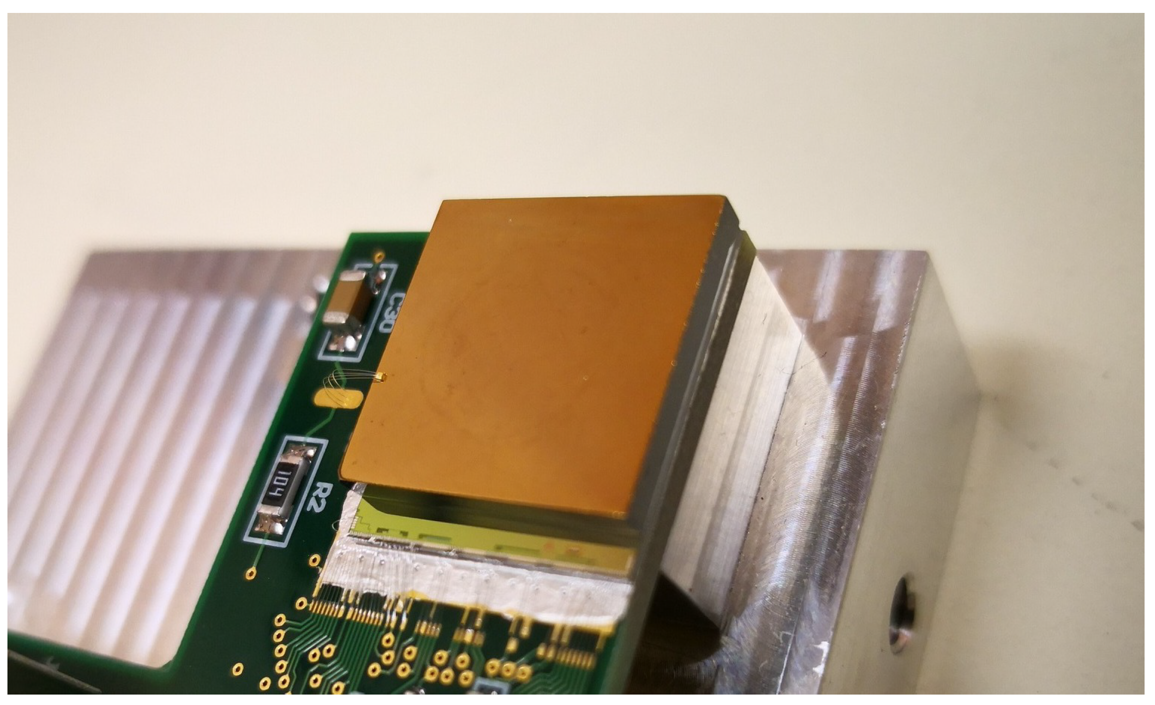
2.2. Detector Assembly
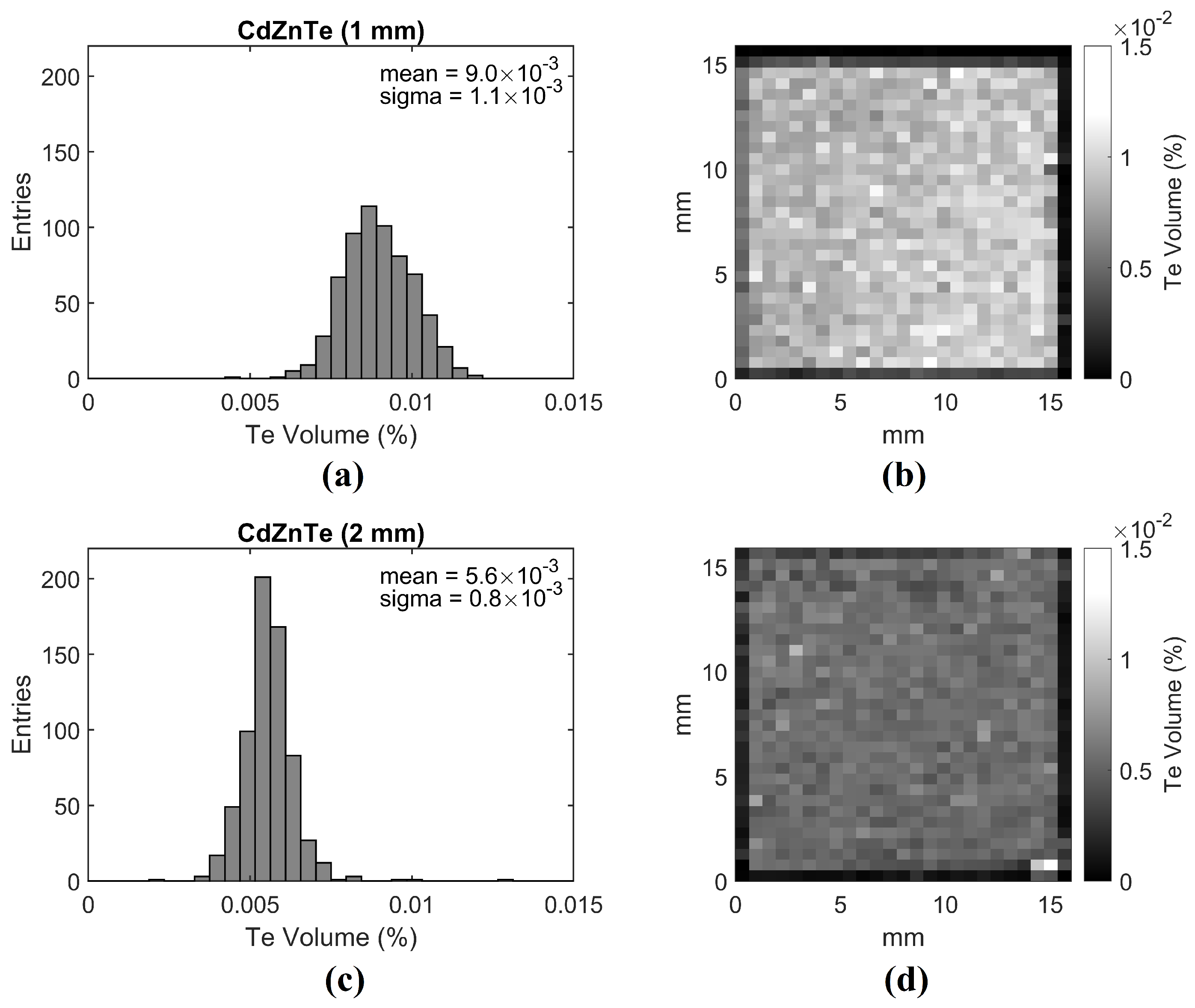
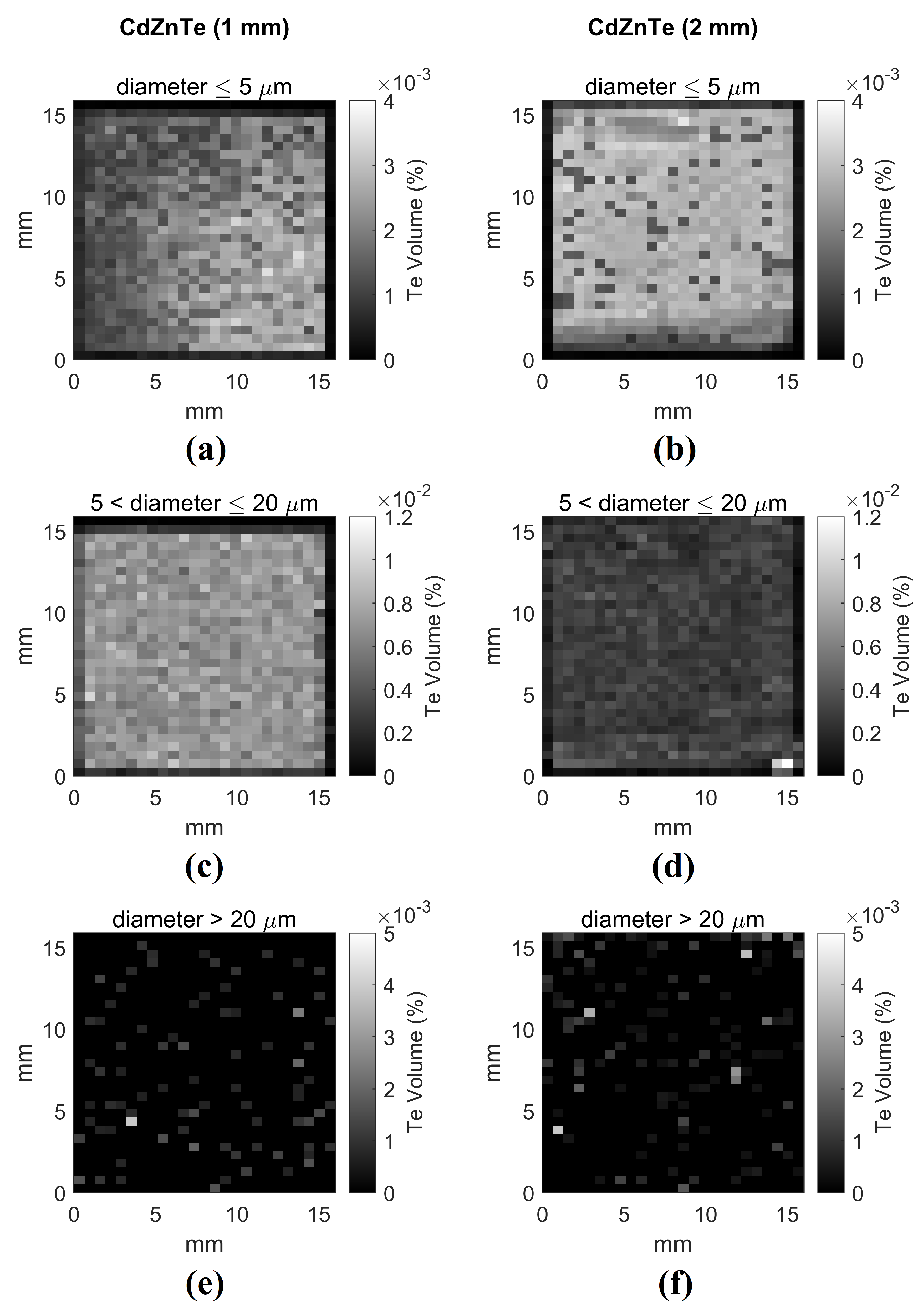
2.3. 3D Inclusion Mapping
2.4. 3D X-ray Detector Response
- Source 1
- A conventional laboratory X-ray generator with exchangeable anodes, able to provide a broad X-ray beam. This source was used for the energy calibration of detector modules. In addition, this source is suitable for basic imaging tests which require uniform illumination and a moderate incoming flux.
- Source 2
- A conventional laboratory X-ray generator featuring a fixed copper (Cu) anode, with the possibility to focus the beam. The beam is initially shaped by focusing optics and then is passing through a set of collimating slits. The final collimation is performed by a circular pinhole that allows configuration of the beam spot size down to 10 . This source is used to perform sensitivity mappings of the sensors at the sub-pixel level or to study the charge transport properties of the sensor material.
3. Results and Discussion
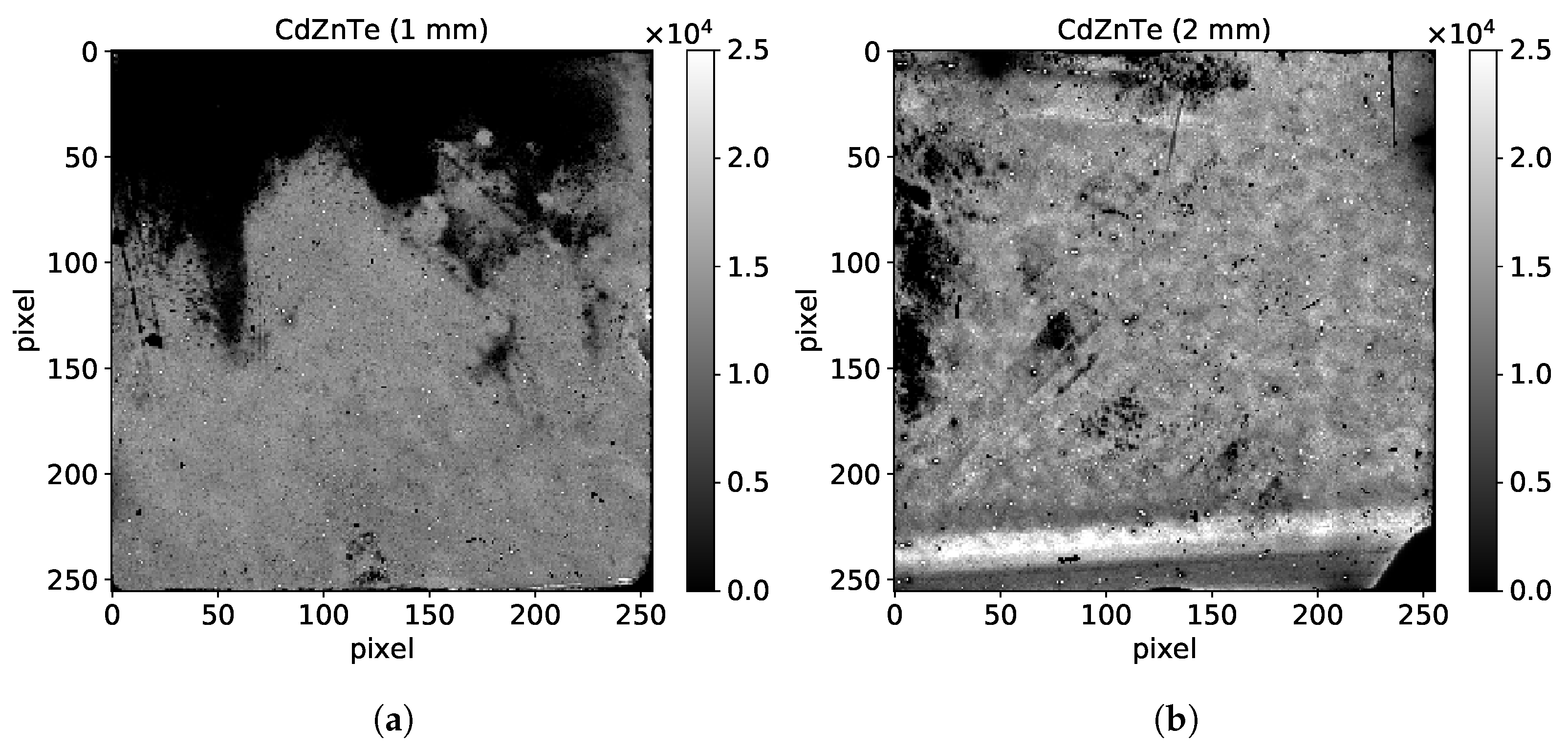
3.1. IR Mapping
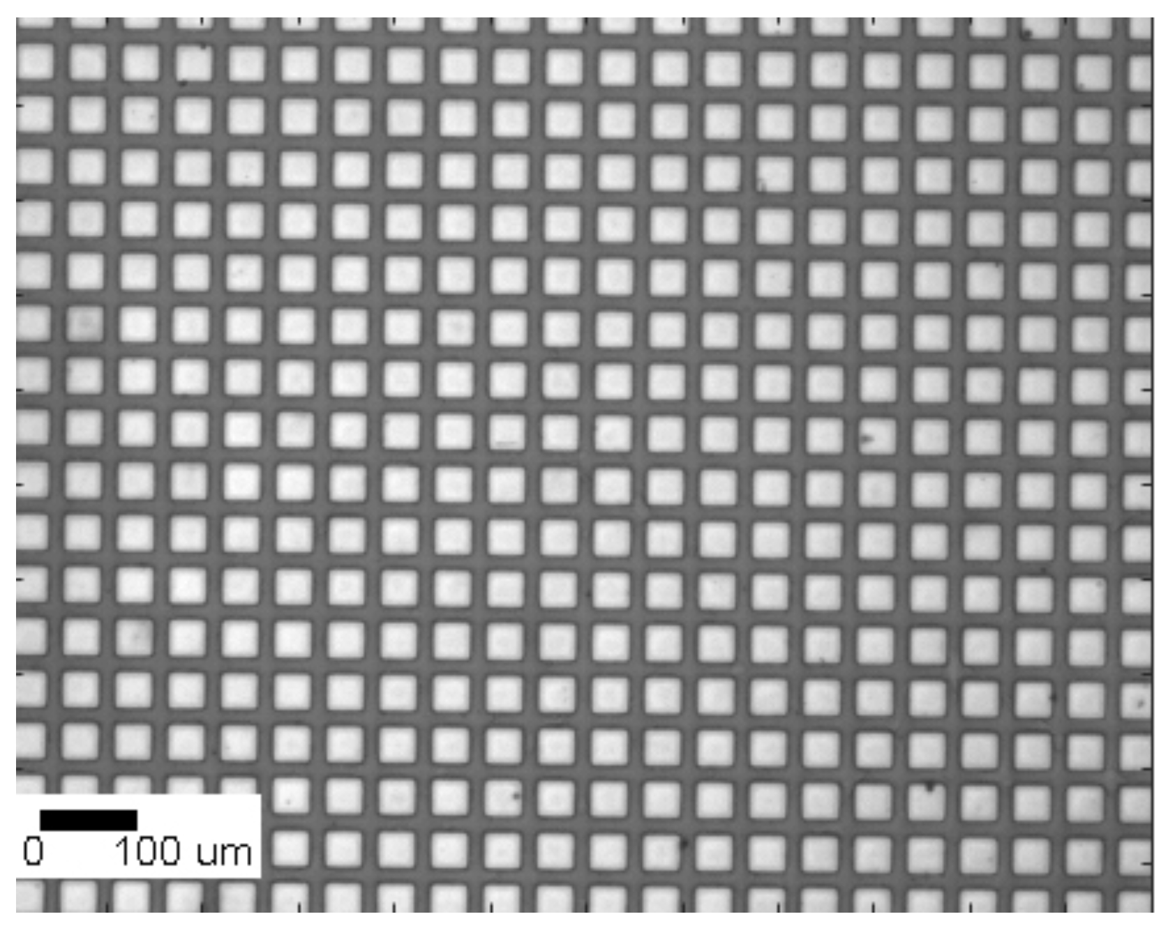
3.2. Visual Inspection
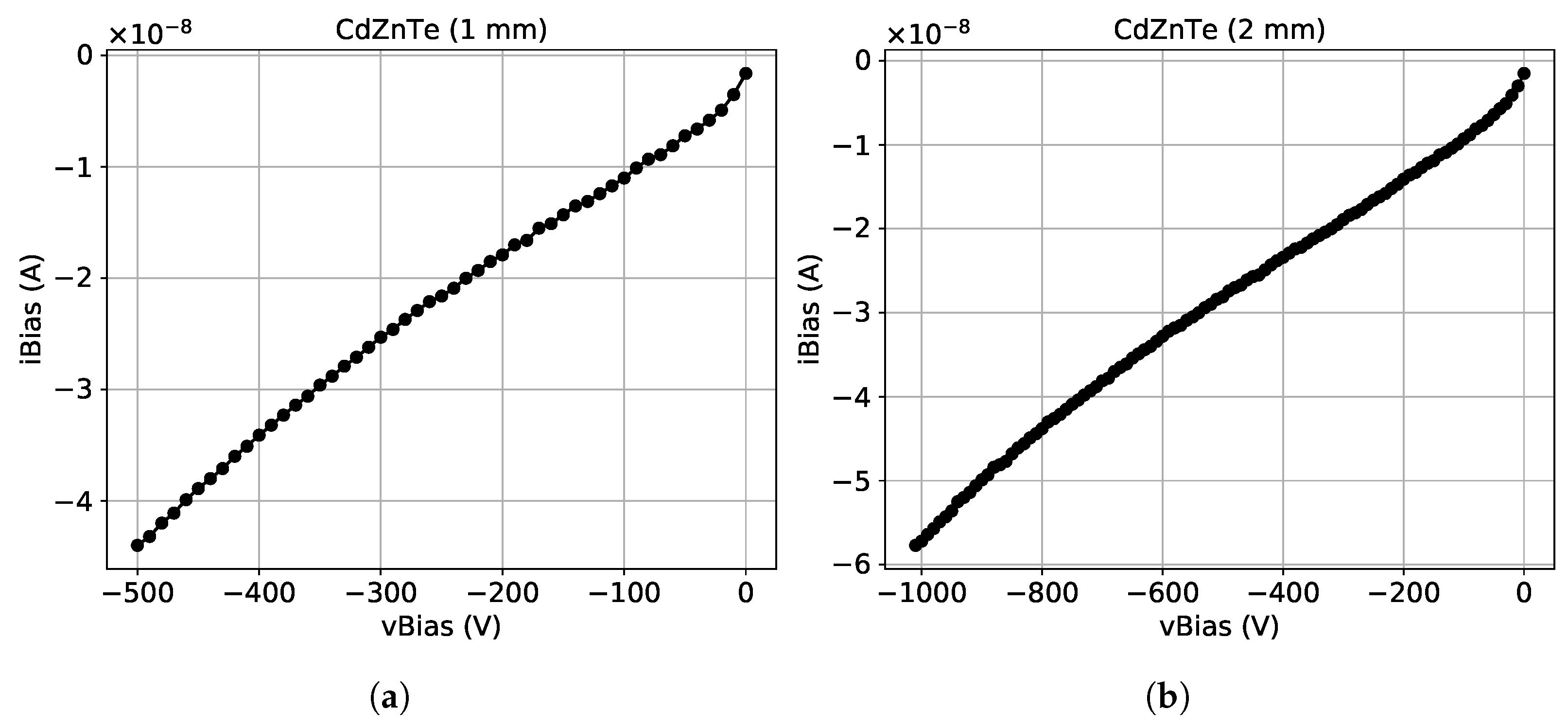
3.3. Electrical Characterization
3.3.1. Before Interconnection
3.3.2. After Interconnection
3.4. Characterization with X-rays
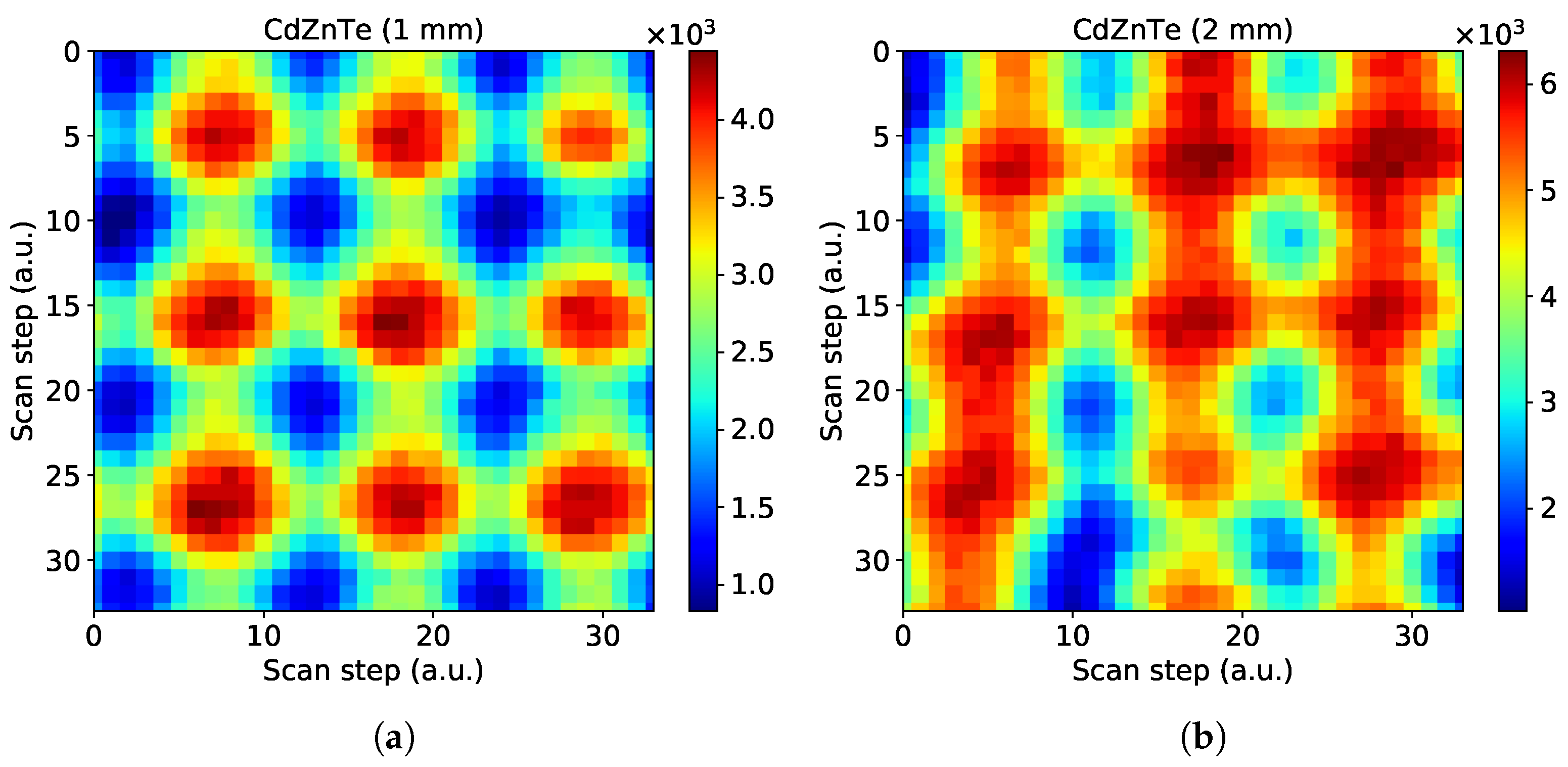
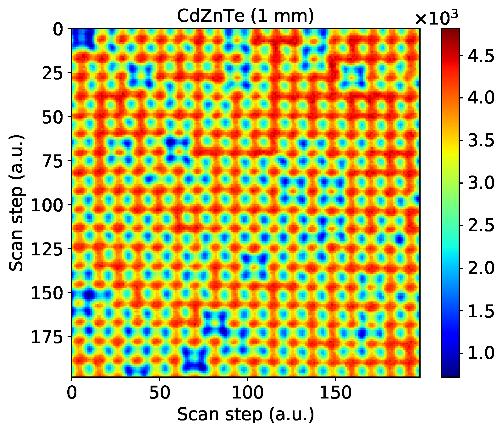
3.4.1. Flood Images
3.4.2. Sub-Pixel Mapping
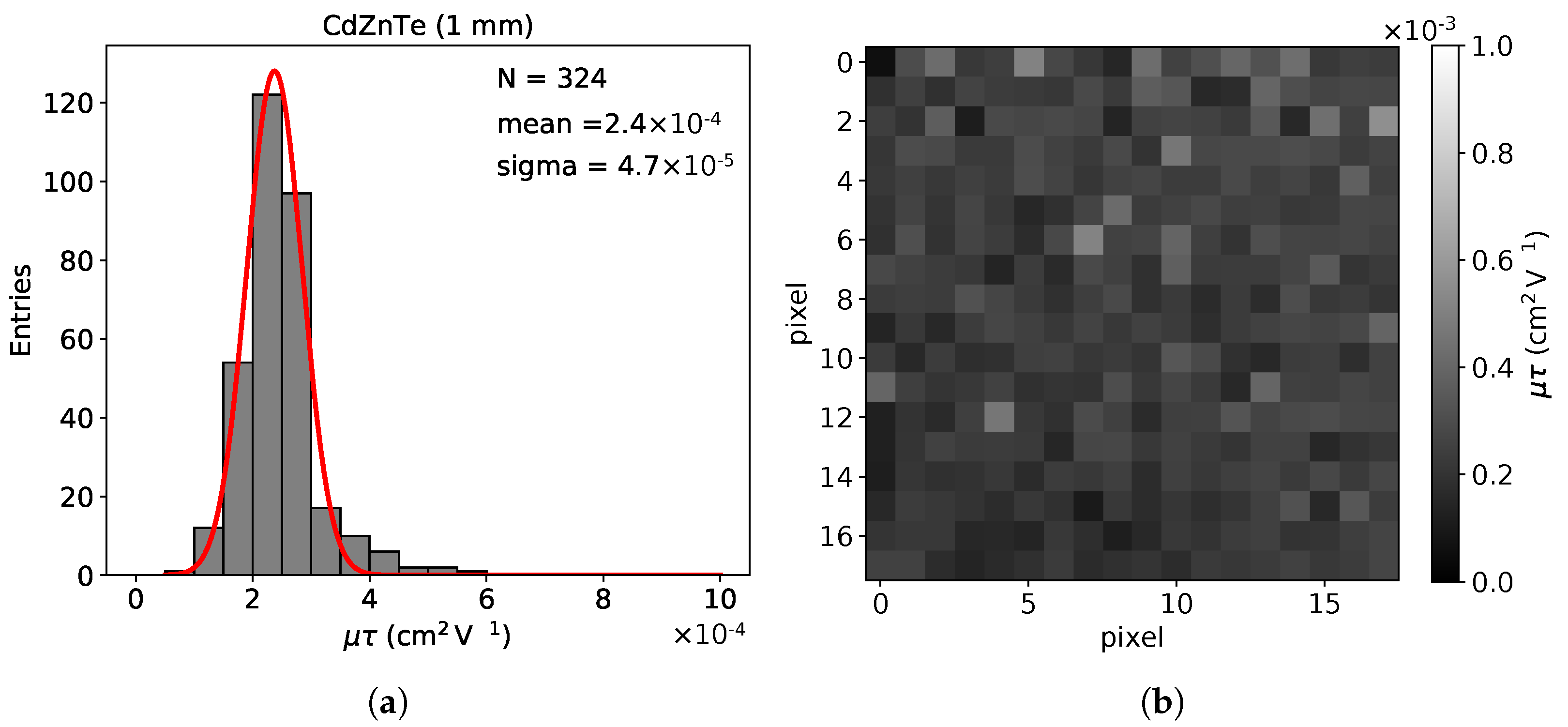
3.4.3. Mobility-Lifetime Product ()
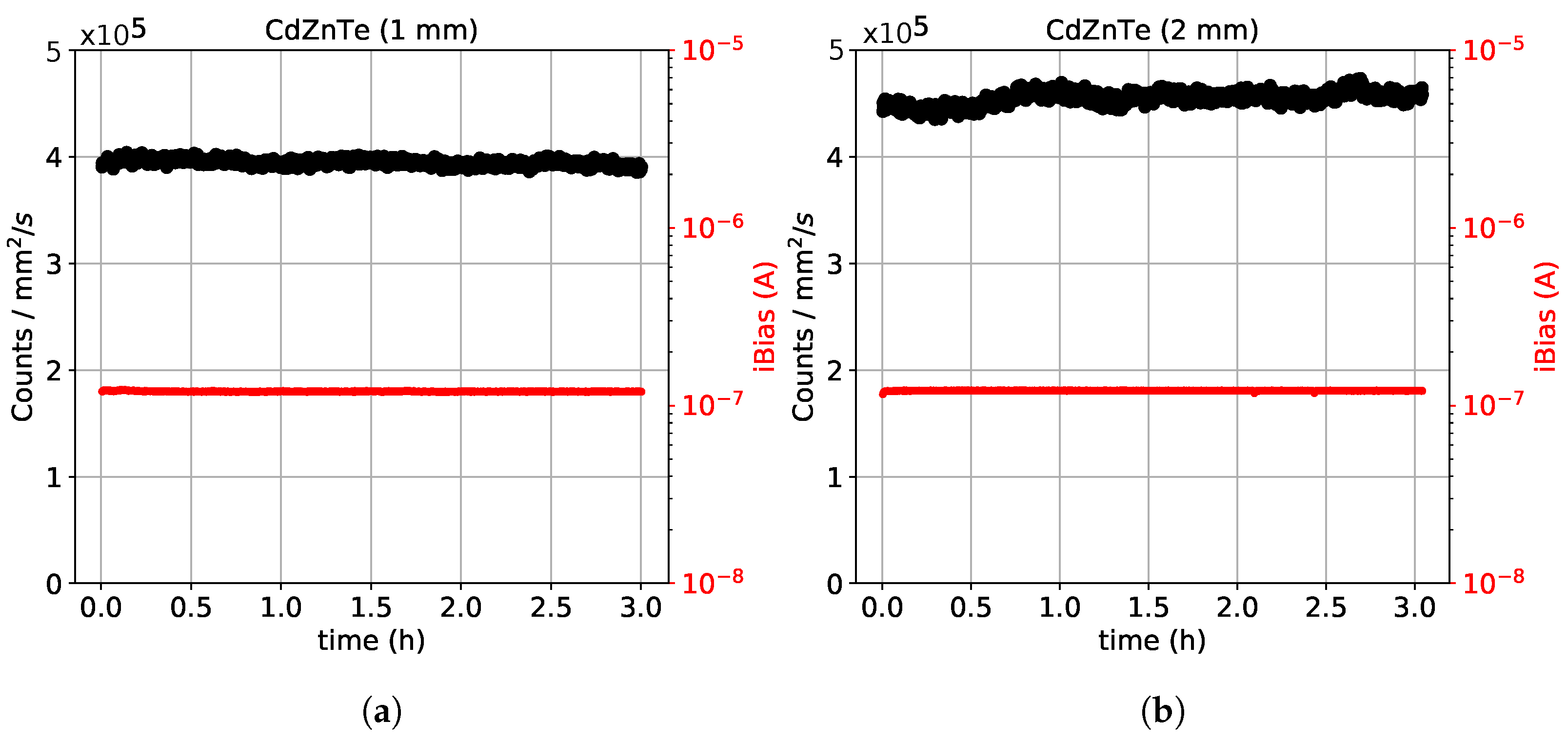
3.4.4. Stability
4. Conclusions
Author Contributions
Funding
Institutional Review Board Statement
Informed Consent Statement
Data Availability Statement
Conflicts of Interest
Abbreviations
| GaAs | Gallium Arsenide |
| CdTe | Cadmium Telluride |
| CdZnTe | Cadmium Zinc Telluride |
| XFEL | X-ray Free Electron Lasers |
| ESRF | European Synchrotron Radiation Facility |
| IMEM-CNR | Istituto dei Materiali per l’Elettronica ed il Magnetismo-Consiglio Nazionale delle Ricerche |
| PCB | Printed Circuit Board |
| ASIC | Application Specific Integrated Circuit |
| ToT | time-over-threshold |
References
- Ballabriga, R.; Alozy, J.; Campbell, M.; Frojdh, E.; Heijne, E.; Koenig, T.; Llopart, X.; Marchal, J.; Pennicard, D.; Poikela, T.; et al. Review of hybrid pixel detector readout ASICs for spectroscopic X-ray imaging. J. Instrum. 2016, 11, P01007. [Google Scholar] [CrossRef]
- Greiffenberg, D.; Andrä, M.; Barten, R.; Bergamaschi, A.; Brückner, M.; Busca, P.; Chiriotti, S.; Chsherbakov, I.; Dinapoli, R.; Fajardo, P.; et al. Characterization of Chromium Compensated GaAs Sensors with the Charge-Integrating JUNGFRAU Readout Chip by Means of a Highly Collimated Pencil Beam. Sensors 2021, 21, 1550. [Google Scholar] [CrossRef] [PubMed]
- Fey, J.; Procz, S.; Schuetz, M.; Fiederle, M. Investigations on performance and spectroscopic capabilities of a 3 mm CdTe Timepix detector. Nucl. Instrum. Methods A 2020, 977, 164–308. [Google Scholar] [CrossRef]
- Gädda, A.; Winkler, A.; Ott, J.; Härkönen, J.; Karadzhinova-Ferrer, A.; Koponen, P.; Luukka, P.; Tikkanen, J.; Vähänen, S. Advanced processing of CdTe pixel radiation detectors. J. Instrum. 2017, 12, C12031. [Google Scholar] [CrossRef]
- Del Sordo, S.; Abbene, L.; Caroli, E.; Mancini, A.M.; Zappettini, A.; Ubertini, P. Progress in the Development of CdTe and CdZnTe Semiconductor Radiation Detectors for Astrophysical and Medical Applications. Sensors 2009, 9, 3491–3526. [Google Scholar] [CrossRef] [PubMed]
- Cola, A.; Farella, I. The polarization mechanism in CdTe Schottky detectors. Appl. Phys. Lett. 2009, 94, 102113. [Google Scholar] [CrossRef]
- Ruat, M.; Ponchut, C. Defect signature, instabilities and polarization in CdTe X-ray sensors with quasi-ohmic contacts. J. Instrum. 2014, 9, C04030. [Google Scholar] [CrossRef]
- Chen, H.; Awadalla, S.A.; Marthandam, P.; Iniewski, K.; Lu, P.H.; Bindley, G. CZT device with improved sensitivity for medical imaging and homeland security applications. In Proceedings of the Hard X-ray, Gamma-ray, and Neutron Detector Physics XI, San Diego, CA, USA, 3–6 August 2009; James, R.B., Franks, L.A., Burger, A., Eds.; International Society for Optics and Photonics: Bellingham, WA, USA, 2009; Volume 7449, pp. 15–31. [Google Scholar] [CrossRef]
- Richtsmeier, D.; Guliyev, E.; Iniewski, K.; Bazalova-Carter, M. Contaminant detection in non-destructive testing using a CZT photon-counting detector. J. Instrum. 2021, 16, P01011. [Google Scholar] [CrossRef]
- Tang, J.; Kislat, F.; Krawczynski, H. Cadmium Zinc Telluride detectors for a next-generation hard X-ray telescope. Astropart. Phys. 2021, 128, 102563. [Google Scholar] [CrossRef]
- Iniewski, K. CZT detector technology for medical imaging. J. Instrum. 2014, 9, C11001. [Google Scholar] [CrossRef]
- Iniewski, K. CZT sensors for Computed Tomography: From crystal growth to image quality. J. Instrum. 2016, 11, C12034. [Google Scholar] [CrossRef]
- Fiederle, M.; Procz, S.; Hamann, E.; Fauler, A.; Fröjdh, C. Overview of GaAs und CdTe Pixel Detectors Using Medipix Electronics. Cryst. Res. Technol. 2020, 55, 2000021. [Google Scholar] [CrossRef]
- Winkler, A.; Naaranoja, T.; Gädda, A.; Ott, J.; Luukka, P.; Karadzhinova-Ferrer, A.; Kalliokoski, M.; Härkönen, J. Optical and electrical characterization of Cadmium Telluride X-ray pad detectors. Nucl. Instrum. Methods A 2019, 924, 28–32. [Google Scholar] [CrossRef]
- Tsigaridas, S.; Ponchut, C.; Zanettini, S.; Zappettini, A. Characterisation of pixelated CdZnTe sensors using MAXIPIX. J. Instrum. 2019, 14, C12009. [Google Scholar] [CrossRef]
- Veale, M.C.; Booker, P.; Cross, S.; Hart, M.D.; Jowitt, L.; Lipp, J.; Schneider, A.; Seller, P.; Wheater, R.M.; Wilson, M.D.; et al. Characterization of the Uniformity of High-Flux CdZnTe Material. Sensors 2020, 20, 2747. [Google Scholar] [CrossRef]
- Bell, S.; Baker, M.; Duarte, D.; Schneider, A.; Seller, P.; Sellin, P.; Veale, M.; Wilson, M. Performance comparison of small-pixel CdZnTe radiation detectors with gold contacts formed by sputter and electroless deposition. J. Instrum. 2017, 12, P06015. [Google Scholar] [CrossRef]
- Tsigaridas, S.; Ponchut, C. X-ray imaging with high-Z sensors for the ESRF-EBS Upgrade. J. Instrum. 2019, 14, C04009. [Google Scholar] [CrossRef]
- Veale, M.C.; Angelsen, C.; Booker, P.; Coughlan, J.; French, M.J.; Hardie, A.; Hart, M.; Lipp, J.; Nicholls, T.; Schneider, A.; et al. Cadmium zinc telluride pixel detectors for high-intensity X-ray imaging at free electron lasers. J. Phys. D Appl. Phys. 2018, 52, 085106. [Google Scholar] [CrossRef]
- Abbene, L.; Gerardi, G.; Turturici, A.; Raso, G.; Benassi, G.; Bettelli, M.; Zambelli, N.; Zappettini, A.; Principato, F. X-ray response of CdZnTe detectors grown by the vertical Bridgman technique: Energy, temperature and high flux effects. Nucl. Instrum. Methods A 2016, 835, 1–12. [Google Scholar] [CrossRef]
- Abbene, L.; Principato, F.; Gerardi, G.; Buttacavoli, A.; Cascio, D.; Bettelli, M.; Amadè, N.S.; Seller, P.; Veale, M.C.; Fox, O.; et al. Room-temperature X-ray response of cadmium–zinc–telluride pixel detectors grown by the vertical Bridgman technique. J. Synchrotron Radiat. 2020, 27, 319–328. [Google Scholar] [CrossRef]
- Zha, M.; Zappettini, A.; Calestani, D.; Marchini, L.; Zanotti, L.; Paorici, C. Full encapsulated CdZnTe crystals by the vertical Bridgman method. J. Cryst. Growth 2008, 310, 2072–2075. [Google Scholar] [CrossRef]
- Zappettini, A.; Görög, T.; Zha, M.; Zanotti, L.; Zuccalli, G.; Paorici, C. A new process for synthesizing high-purity stoichiometric cadmium telluride. J. Cryst. Growth 2000, 214–215, 14–18. [Google Scholar] [CrossRef]
- Zha, M.; Gombia, E.; Bissoli, F.; Zappettini, A.; Zanotti, L. Growth and Deep Level Characterisation of Undoped High Resistivity CdTe Crystals. Phys. Status Solidi 2002, 229, 15–18. [Google Scholar] [CrossRef]
- Benassi, G.; Nasi, L.; Bettelli, M.; Zambelli, N.; Calestani, D.; Zappettini, A. Strong mechanical adhesion of gold electroless contacts on CdZnTe deposited by alcoholic solutions. J. Instrum. 2017, 12, P02018. [Google Scholar] [CrossRef]
- Llopart, X.; Ballabriga, R.; Campbell, M.; Tlustos, L.; Wong, W. Timepix, a 65k programmable pixel readout chip for arrival time, energy and/or photon counting measurements. Nucl. Instrum. Methods A 2007, 581, 485–494. [Google Scholar] [CrossRef]
- Ponchut, C.; Rigal, J.M.; Clément, J.; Papillon, E.; Homs, A.; Petitdemange, S. MAXIPIX, a fast readout photon-counting X-ray area detector for synchrotron applications. J. Instrum. 2011, 6, C01069. [Google Scholar] [CrossRef]
- Marchini, L.; Zappettini, A.; Zha, M.; Zambelli, N.; Bolotnikov, A.E.; Camarda, G.S.; James, R.B. Crystal Defects in CdZnTe Crystals Grown by the Modified Low-Pressure Bridgman Method. IEEE Trans. Nucl. Sci. 2012, 59, 264–267. [Google Scholar] [CrossRef]
- Bolotnikov, A.E.; Abdul-Jabbar, N.M.; Babalola, O.S.; Camarda, G.S.; Cui, Y.; Hossain, A.M.; Jackson, E.M.; Jackson, H.C.; James, J.A.; Kohman, K.T.; et al. Effects of Te Inclusions on the Performance of CdZnTe Radiation Detectors. IEEE Trans. Nucl. Sci. 2008, 55, 2757–2764. [Google Scholar] [CrossRef]
- Zambelli, N.; Marchini, L.; Zha, M.; Zappettini, A. Three-dimensional mapping of tellurium inclusions in CdZnTe crystals by means of improved optical microscopy. J. Cryst. Growth 2011, 318, 1167–1170. [Google Scholar] [CrossRef]
- Zambelli, N.; Zappettini, A. A method and system for the three-dimensional reconstruction of formations dispersed in a matrix of a material, in particular of inclusions in crystalline matrices. Patent no. EP2706505A1, 5 September 2013. [Google Scholar]
- Li, G.; Shih, S.J.; Huang, Y.; Wang, T.; Jie, W. Nanostructures of defects in CdZnTe single crystals. J. Cryst. Growth 2008, 311, 85–89. [Google Scholar] [CrossRef]
- Tsigaridas, S.; Ponchut, C.; Tolbanov, O.; Tyazhev, A.; Zarubin, A. Investigation of thick GaAs:Cr pixel sensors for X-ray imaging applications. J. Instrum. 2021, 16, P01032. [Google Scholar] [CrossRef]


| Source Features | Source 1 | Source 2 |
|---|---|---|
| Anode | Molybdenum (Mo) | Copper (Cu) |
| Peak voltage/Current | 25 /25 | 31 /1 |
| Filtering material | Zirconium (Zr) | Copper (Cu) |
| Filtering thickness | 100 | 50 |
| Characteristic X-ray energy | 17 keV | 8 keV |
Publisher’s Note: MDPI stays neutral with regard to jurisdictional claims in published maps and institutional affiliations. |
© 2021 by the authors. Licensee MDPI, Basel, Switzerland. This article is an open access article distributed under the terms and conditions of the Creative Commons Attribution (CC BY) license (https://creativecommons.org/licenses/by/4.0/).
Share and Cite
Tsigaridas, S.; Zanettini, S.; Bettelli, M.; Amadè, N.S.; Calestani, D.; Ponchut, C.; Zappettini, A. Fabrication of Small-Pixel CdZnTe Sensors and Characterization with X-rays. Sensors 2021, 21, 2932. https://doi.org/10.3390/s21092932
Tsigaridas S, Zanettini S, Bettelli M, Amadè NS, Calestani D, Ponchut C, Zappettini A. Fabrication of Small-Pixel CdZnTe Sensors and Characterization with X-rays. Sensors. 2021; 21(9):2932. https://doi.org/10.3390/s21092932
Chicago/Turabian StyleTsigaridas, Stergios, Silvia Zanettini, Manuele Bettelli, Nicola Sarzi Amadè, Davide Calestani, Cyril Ponchut, and Andrea Zappettini. 2021. "Fabrication of Small-Pixel CdZnTe Sensors and Characterization with X-rays" Sensors 21, no. 9: 2932. https://doi.org/10.3390/s21092932
APA StyleTsigaridas, S., Zanettini, S., Bettelli, M., Amadè, N. S., Calestani, D., Ponchut, C., & Zappettini, A. (2021). Fabrication of Small-Pixel CdZnTe Sensors and Characterization with X-rays. Sensors, 21(9), 2932. https://doi.org/10.3390/s21092932