2.1. Sensor Design
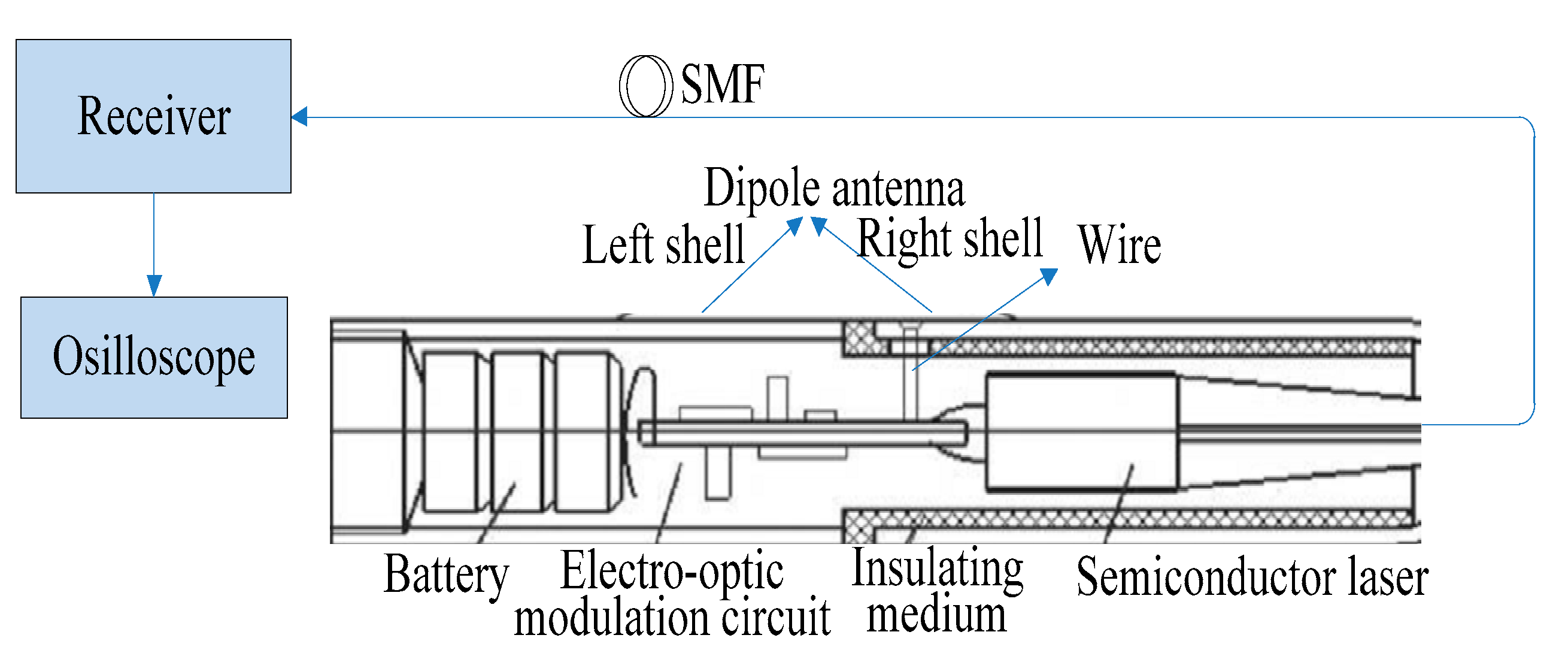
The configuration of the proposed sensor system is shown schematically in
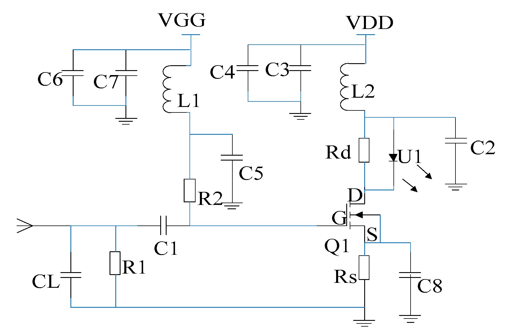
Figure 1. The sensor shell acts not only as the dipole antenna detecting an externally weak EMP field but also shields the battery and the electro-optic modulation circuit shown in
Figure 2.
The entire shell is divided into left and right parts by an insulating medium: The left shell is equivalent to a grounding mechanism, and the right shell plays a different role according to the strength of the EMP field. For the weak field sensor, the right shell is electrically connected with the antenna port of the electro-optic modulation circuit by a wire; in this case, the length of the right shell is similar to length of the left shell, and this kind of shell structure acts as a dipole antenna for detecting small signals. However, when the detected signal is so large that it exceeds the linear range of the FET Q1 and enters into the saturation region of FET Q1, it can cause a distortion of the detected signal. Obviously, the above dipole antenna is not suitable for detecting a strong EMP field. Therefore, the strong field sensor was designed by changing the type of the antenna, and we took a short wire welded at the antenna port of the electro-optic modulation circuit as the mono-pole antenna; here, the right shell is only a shielding shell and not the antenna, and the left shell is still taken as the ground. The two kinds of antenna both belong to an electrically small antenna, which has high resonant frequency and is connected to the grid electrode of the FET Q1 through a attenuation capacitor CL. Moreover, the LD U1 is connected in series with the FET Q1. Due to the fact that the FET is a voltage-controlled current element and has high input resistance, the electric field signal induced by the antenna directly controls the drain current of the FET and realizes the high resistance output of the antenna-received signal, which is the antenna’s high resistance coupling principle of the electric field sensor. According to the analysis theory of the antenna, when the antenna is coupled with high resistance, the operating bandwidth of the antenna is fully utilized, which provides a broadband foundation for a pulse electric field test. The LD is connected in series with the FET; thus, the drain current of the FET becomes the operating current of the semiconductor laser, which realizes the direct drive of the LD by the antenna receiving the electric field signal, and finally achieves a direct conversion between the electric field signal and the modulated optical signal, which widens the bandwidth of the test system from the source. Then, the transmitted optical signal is received by the receiver and converted into an electrical signal, which is displayed by the oscilloscope.
For the proposed direct electro-optic modulation circuit, the amplification, conversion and drive are achieved by only one FET, and the circuit is simplified further on the basis of the literature [
26]. Moreover, this design integrated the antenna and electro-optic modulation together and eliminates the impedance conversion network and amplification-driving circuit that seriously limits the transmission bandwidth; this fundamentally overcomes the problem of the connection between the electro-optic modulator and the antenna. In the electro-optic modulation circuit, the FET adopted an N-channel GaAs MESFET NE72218 produced by NEC company, and
Table 1 presents its electrical characteristics. It can be observed from the
Table 1 that it possesses low phase noise and high power gain, its saturated drain current reaches 120 mA and the cut-off upper frequency reaches up to 12 GHz.
Figure 3b shows the relationship curve between drain current I
D and drain-to-source voltage V
DS under different grid-to-source voltage V
GS; here, V
GS represents the voltage of the input signal received by antenna, and I
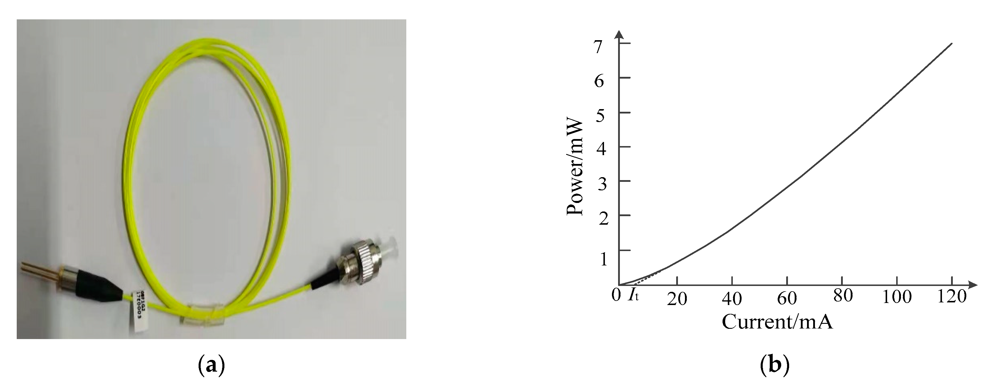
D is used to drive LD. According to the parameters of FET, LD is customized by Jiuzhou company, which is a high-performance uncooled distributed feedback semiconductor laser (DFB–LD) with the wavelength of 1310 nm, an output power of 7 mW and a cut-off frequency of 2.5 GHz; moreover, the physical diagram of the laser is shown in
Figure 4a,b, and the figures show that the laser has a threshold current
It, which is 4.5 mA. When the driving current generated by FET is less than the threshold current, the laser basically does not emit light or only emits very weak spectral lines. Conversely, when the driving current is greater than FET, the laser starts to emit a laser, and the output light intensity increases linearly with the increase in driving current, which is the operating area of electro-optic modulation. The linear region consistency of the two components determines the performance of the sensor.
Therefore, it is essential to set an appropriate static operating point for FET in order to ensure an input electrical signal that works in a linear region.
Figure 3a shows the DC path of electro-optic modulation circuit. The FET Q1 is operated in terms of self bias, and the resistance, Rs, can adjust the self bias of the FET and ensure that the FET is in a suitable linear operating area and set a suitable operating current for the LD. Moreover, a current negative feedback circuit through Rs is presented, which provides a stable operating current for the LD. By conducting several tests, the optimal values of these parameters were determined, which include the following: V
GG = −1.24 V; V
DD = 3.3 V; Rs = 11 Ω; R
1 = 68 MΩ; R
2 = 43 MΩ; R
d = 3.3 Ω; I
DQ = 28 mA; and U
GSQ and U
DSQ are calculated by Equations (1) and (2) and equal −1.07 V and 2.1 V, respectively. The static operating point can be observed in
Figure 3b.
The measurement range of the sensor is mainly determined by the threshold current It of LD and the saturated drain current IDSS of the FET. It corresponds to the minimum electric field strength and determines that FET is always in the amplification region. Due to the fact that the output power of LD has a large transient allowable value, IDSS represents the maximum electric field strength. By taking the static operating point Q of the FET as a reference point, when the input voltage in the grid electrode of FET was changed from −0.635 V to +0.635 V (that is, the AC signal is superimposed on the basis of UGSQ), the maximum and minimum grid-to-source voltages are −0.81 V and −2.08 V, respectively; at the same time, the maximum and minimum drain currents are 4.5 mA and 120 mA, respectively. Hence, the corresponding output optical power range of LD is 0–7 mW. In this case, the sensor can measure negative and positive pulses in an undistorted manner. For the case of only negative pulse or positive pulse, UGSQ can be adjusted by R1, R2, Rs and VGG to increase or decrease, and the measurement range of 0–1.27 V can be achieved when UGSQ is assumed at −2.08 V. Similarly, when UGSQ is set at −0.81 V, the negative pulse with voltage varying from −1.27 V to 0 V could be measured. In addition, when the input voltage is greater than the above measurement range, the appropriate attenuation capacitor CL is needed, which can be further broaden the measurement range, and the factor depends on the equivalent capacitance of antenna Cant and its capacitance value.
2.2. Analytic Model
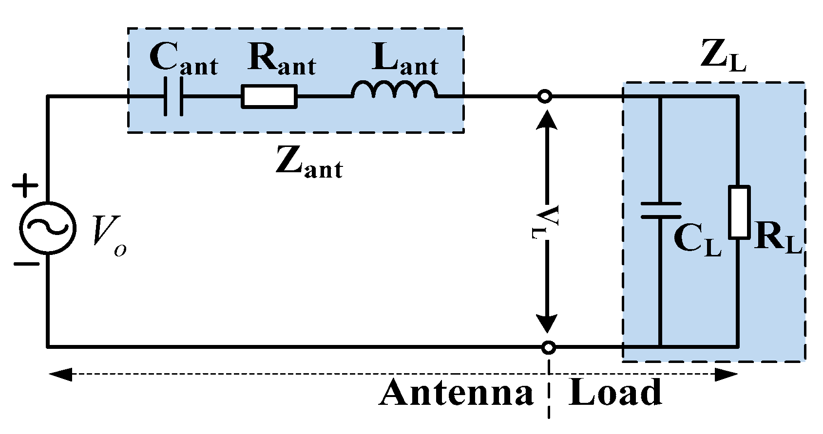
In order to analyze the influence of various parameters on the impedance of antenna and its terminal load comprehensively, the equivalent circuit of an electric field sensor was established, as shown in
Figure 5.
Cant,
Rant and
Lant are the equivalent capacitance, resistance and inductance of antenna, respectively.
RL and
CL are the resistance and capacitance of loads.
The voltage of load
VL is calculated in the
S domain and expressed as transfer function G(
s).
In the low frequency band, the second-order pole in Equation (3) is far greater than (1 +
sRLCL) (that is,
s2LantCant << 1,
sRantCant << 1), and Equation (3) can be simplified as follows.
The above equation is regarded as a high-pass filter for which its lower cut-off frequency
fL can be written as follows.
In the high frequency band, Equation (3) can be simplified as a second-order low-pass filter:
where ω
0 = ((
Cant +
CL)/(
CLCant Lant))
1/2 is the undamped angular frequency of the second-order system, and ζ =
Rant/(2
Lantω
0) is the damping ratio. Suppose
s =
jw,
u =
w/
w0; then, Equation (6) can be written as follows.
The amplitude and phase characteristics are given, respectively, as follows.
According to Equation (8), the high-frequency response characteristic curve is drawn in
Figure 6. When 0 < ζ < 0.707, the upper cut-off frequency
fH can be expanded, but the resonance spike in the curve will appear, and its peak value
Mr increases with a decrease in ζ. By setting
d/
du|G(
u)| as 0, the resonant frequencies
fr and
Mr can be derived as follows [
28].
According to the definition of −3 dB bandwidth, suppose |G(
u)| = 0.707 ×
Cant/(
Cant +
CL); then, its upper cut-off frequency
fH can be described as follows.
It can be observed from
Figure 6 that there is no resonance spike in the curve, and the curve rolls down rapidly at the upper cut-off frequency when ζ is greater than or equals 0.707. In particular, when ζ equals 0.707, the flat section of the amplitude frequency characteristic curve is the widest, and the phase frequency characteristic curve is close to an oblique line; thus, it is usually called the best damping ratio. In this case,
fH equals
f0 according to Equation (11); thus, its upper cut-off frequency
fH can be simplified into the following.
When the frequency
f in the transient electric field to be measured is between
fL and
fH, the time domain output of antenna
VL(
t) on the terminal load can be written as follows:
where C
ant = h/(60 ×
c × (2 × ln(2 × h/a) − 2 − ln4)),
h is the length of antenna,
a is the radius of antenna and c is the propagation velocity of electromagnetic wave.
2.3. Simulation Nalysis
By taking the cylindrical electrically small dipole antenna as an example, the influence of the parameters such as the size of the antenna and its termination load on the frequency response of the sensor is further studied. The input impedance
Zant of the antenna is expressed as follows:
where
Z0 = 120 × (ln(2 ×
h/
a) − 1), which is the average characteristic impedance of the antenna;
η = 73.1 × (
Z0 ×
h × (1 − sin(2 ×
h ×
k)/(2 ×
h ×
k))), which is the attenuation constant of the equivalent transmission line after considering radiation loss; and
k =
ω/
c, which is the wave number.
According to the equivalent circuit model in
Figure 2, the relationship between
VL and
Vo is written in the form of a transfer function, and its frequency domain expression is described as follows:
where
ZL(
ω) = R
L/(1 +
jω ×
RL ×
CL).
The simulation results of frequency and time domain characteristic of the sensor under the different size of antenna and load resistance are given in
Figure 7,
Figure 8 and
Figure 9. The length and radius of the antenna are fixed at 30 mm and 3 mm, respectively, changing the value of
RL, i.e., 50 Ω, 1 kΩ and 1 MΩ, and
CL, i.e., 1 pF, 10 pF and 50 pF. The frequency characteristics of the sensor were analyzed based on Equations (14) and (15), which can be observed from
Figure 7a.
It can be observed from
Figure 7a that the change of
RL and
CL can obviously affect the low-frequency characteristic of the sensor, but it has little influence on its high-frequency characteristic. By fixing
RL at 1 MΩ and increasing
CL from 1 pF to 50 pF by a certain step, the lower cut-off frequency moves towards the direction of low-frequency; this trend broadens the bandwidth of sensor, but the cost is a decrease in gain. Conversely, by fixing
CL at 50 pF and increasing
RL from 50 Ω to 1 MΩ by a certain step, in this case, the change trend of the lower cut-off frequency is similar to the above case, and the only difference is that the gain does not decrease but retains a fixed value, which agrees with the theoretical calculation of the sensor’s lower-frequency in
Section 2.2. Furthermore, assuming that
RL is 1 MΩ and
CL is 10 pF, when the size of antenna is changed, the effect on the frequency characteristic of the sensor can be observed from
Figure 7b, and the result shows that the change of the antenna’s length and radius generates a distinct influence on the upper cut-off frequency of the sensor but has little effect on its lower cut-off frequency. Furthermore, when the radius
a of antenna is maintained at 50 mm, increasing the length
h of antenna causes the gain of the sensor to also increase, but the upper cut-off frequency obviously decreases. On the other hand, when the length
h of antenna is fixed at 1 mm, increasing the radius
a of the antenna causes the gain of the sensor to also increase, but its lower and upper cut-off frequencies do not experience significant change. Meanwhile, compared with the resonance spike of these curves in
Figure 7b, it can be observed that the resonance peak of the curve becomes more obvious with an increase in
h; that is, the damping ratio ζ shows a decreasing trend. However, with an increase in
a, the curve of the frequency response tends to be flat, and the damping ratio ζ has an increasing trend, which means that the physical size of antenna can affect damping ratio ζ. Therefore, by optimizing the design of antenna, the frequency response characteristic curves with maximum flatness can be obtained.
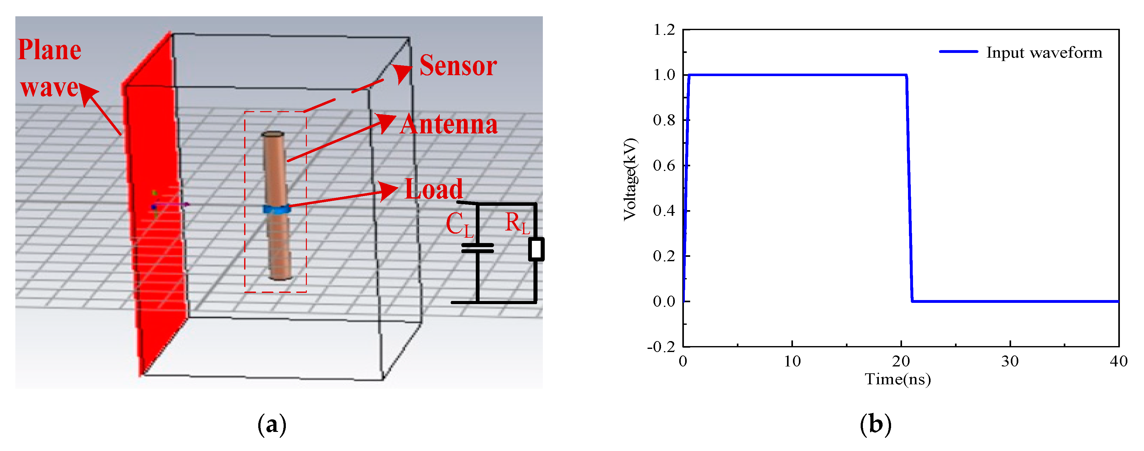
For the dipole antenna as an example, the simulation model of the sensor was established (as observed in
Figure 8a). The material of the antenna is set as PEC, i.e., ideal conductor material, which is placed 1 m away from the incident plane wave, and the termination load is a circuit of
RL in parallel with
CL. Considering that the square pulse with a sharp edge has rich low frequency and high frequency components (that is, its response can directly reflect the performance of the sensor), the square pulse with 1 kV of the voltage peak, 0.5 ns of rise time and 20 ns of the pulse width was selected as the excitation signal (see
Figure 8b), which can form a plane wave environment with 1 kV/m of EMP field strength at the position where the sensor was placed. In this case,
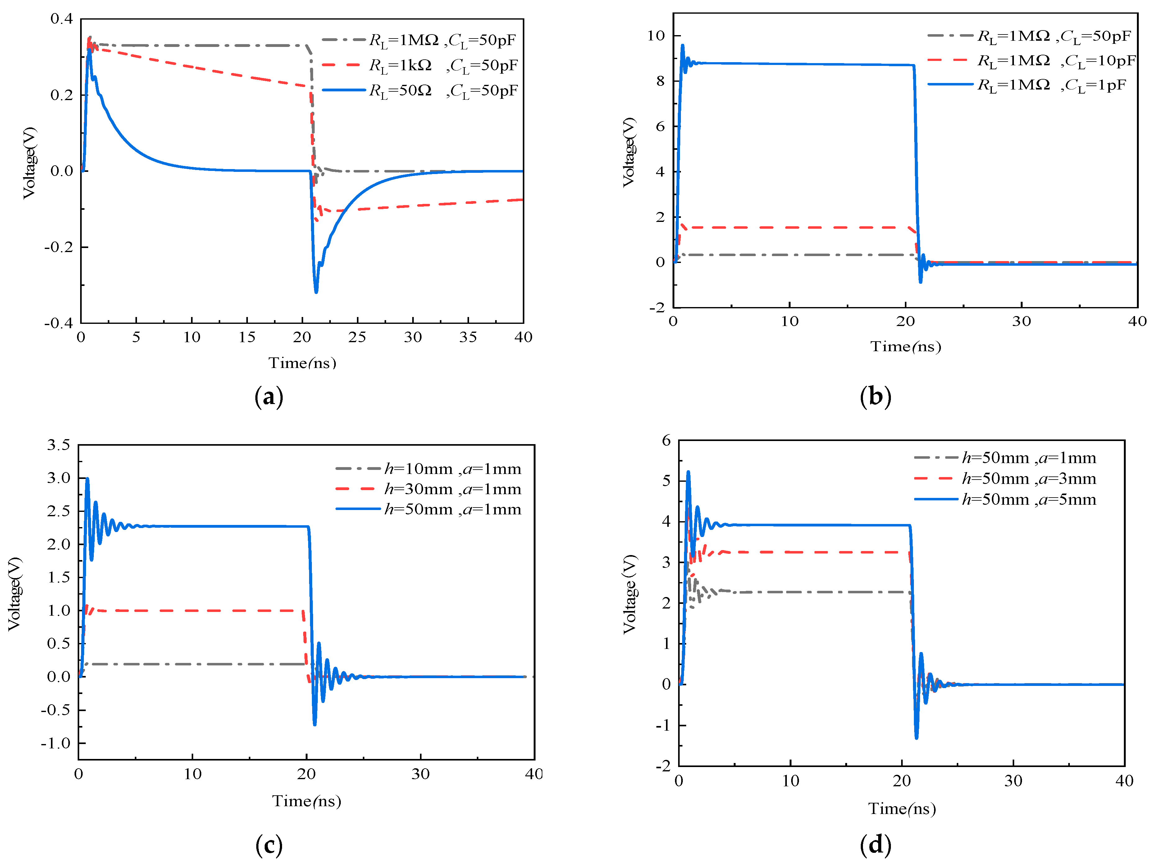
Figure 9 shows the pulse responses of loads under different load resistances when
h is 30 mm and
a is 3 mm and the different sizes of the antenna when
RL is 1 MΩ and
CL is 10 pF.
It can be observed from
Figure 9a that the response waveform of the sensor incurs obvious flattop declines when
RL is 50 Ω and
CL is 50 pF, which is similar to the differential waveform of square pulses. This case demonstrates that the sensor possesses bad responses characteristic of lower cut-off frequencies. With an increase in
RL, the response waveform becomes better, and the excitation signal can be restored correctly, except for the attenuation on magnitude when
RL is 1 MΩ. In this case, by increasing capacitance
CL, its magnitude will decrease gradually. As a result, a greater
RL can reduce the lower cut-off frequency of the sensor effectively, and a lower
CL can improve its gain (see
Figure 9b). Moreover,
Figure 9c shows that the gain of the sensor will obviously increase with an increase in the antenna’s length
h or radius
a. Furthermore, when
a is fixed to 1mm and the length
h of antenna is increased, a larger vibration occurs at the positions of the rising and falling edge. However, as shown in
Figure 9d, the vibration of the edge cannot be improved by changing radius
a. Therefore, the degree of edge’s vibration, i.e., the higher upper cut-off frequency of sensor, mainly depends on length
h of antenna.
2.4. Selection of Key Parameters
On the basis of the above analysis, fL can be reduced by increasing RL, CL and Cant. The increase in Cant results in a decrease in its resonant frequency, which limits the high-frequency response characteristics of the sensor. Generally, in order to expand fH, Cant was designed to be relatively small (several pF). The value of CL mainly depends on input capacitance and parasitic capacitance of the load circuit. It can be observed from simulation results that an increase in CL reduces the output gain and affects the high frequency performance of the sensor. Therefore, the method of increasing RL is used to reduce fL. If we need to satisfy the condition that fL is less than 100 kHz, where CL + Cant equals to 100 pF approximately, then the value of RL must be greater than 106 Ω.
It can be observed from Equation (12) that
fH is greatly affected by
Cant,
Lant and
CL. Reducing these parameters can improve
fH. This shows that the physical characteristics of the antenna itself such as its length
h and radius
a have a great influence on the high-frequency response characteristics of the electric field sensor. According to the theory of the antenna, the maximum upper cut-off frequency
fhm of the sensor can be satisfied as follows.
Therefore, if
fH is required to reach 1 GHz, then
h should be less than 60 mm. Moreover, in order to decrease the influence of the parasitic parameter, a miniature circuit design is adopted for the PCB layout of the electro-optic modulation circuit shown in
Figure 10a.
Figure 10b,c show the photographs of two sensors. For the weak field sensor, the right part of the shielding shell acts as an antenna (see
Figure 10b). Its package size is
Φ 13 mm × 70 mm,
h is 35 mm,
a is 6.5 mm and
RL equals R1/R2, which is 26 MΩ. For the strong field sensor, the wire acts as an antenna (see
Figure 10c). Its length can be easily adjusted. Here, the package size is Φ 13 mm × 60 mm,
h is 3 mm,
a is 0.5 mm,
CL is 100 pF and
RL is also 26 MΩ. The designed strong field sensor can measure higher fields and has a wider measurement range. Conversely, the designed weak field sensor tends to improve sensitivity at the cost of reducing the measurement range, which can be used to test the very low field strength by removing attenuation capacitance C
L. Due to the fact that these circuits use less dissipative elements, a 3.7 V battery can be guaranteed for the normal operation of the circuit for several hours.
