1. Introduction
Magnetic sensors (MSs) have a wide range of uses and can be applied in control and monitoring devices, industrial products, material testing, manufacturing systems and biomedical engineering. For instance, Lu [
1] used a microelectromechanical system (MEMS) MS to develop a location tracking system that was applied in real-time tracking of the vessel location and organ shape for surgical navigation. The location tracking system provided a magnetic field (MF) to a patient and employed the MS node to detect the organ location of the patient. Lee [
2] utilized a 3 × 3 array of Hall MSs to construct an MF measurement system for MF mapping. The system could measure the MF distributions of a group of multi-magnets. Oh [
3] adopted a small magnet, an MEMS MS and a breathing output component to compose a respiratory monitoring and training system that was used to train and monitor the breath of patients for radiotherapy. Lara-Castro [
4] employed a micromachined MS to constitute a portable signal conditioning system for industrial applications to measure ferromagnetic material characteristic. The MS was composed of a silicon resonator, an aluminum loop and four piezoresistors. Krishnapriya [
5] manufactured a micro MS with a planar micro coil for biomedical application to detect biomolecules and pathogens. An integrated microfluidic platform, proposed by Feng [
6], was assembled by a micro MS and a micro-spiral planar coil. The microfluidic platform was used to detect and manipulate magnetic beads. Zhang [
7] designed a magnetic scanning device with a digital micro MS. The magnetic scanning device, which was a non-destructive test, could detect the leakage of MF from steel corrosion in reinforced concrete. An unmanned aerial vehicle (UAV) navigation system, presented by Vetrella [
8], was built using an MEMS MS, a global positioning system receiver, an inertial sensor, a navigation algorithm and a vision component. The system was utilized to control and stabilize the UAV flight.
The advantages of micro MS are that is has a small volume, easy integration and a high performance. Recently, the MEMS technology was adopted to design and fabricate various micro MSs.
Table 1 summarizes the sensing principle and type for various micro magnetic sensors. For example, an MS, as proposed by Niekiel [
9], was fabricated using the MEMS technology. The MEMS MS, which was a magnetic-resonant type, contained a piezoelectric resonator that integrated permanent magnets. Chen [
10] developed a MEM MS, which was a giant magneto-impedance type, using surface micromachining. The magnetic sensing material for the sensor was the copper-based amorphous wire. The sensor had a micro coil which surrounded the copper-based amorphous wire, and the output signal for the sensor was produced by the micro coil. The sensitivity of the MEMS MS was 130 mV/Oe. A MEMS MS that was a magnetic-resonant type was presented by Okada [
11]. The sensor had a resonator and a micro bridge. The resonator was a silicon bridge with a PZT thin film, and the micro bridge was silicon with a FePd film. When an MF was applied to the micro bridge it produced a deflection to act on the resonator, so that the stiffness of the resonator changed, which lead to a variation in the resonance frequency of the resonator. Guo [
12] made an MEMS MS that was a fluxgate type using the micromachining with chemical wet etching. The MEMS MS had a double-layer magnetic core that was deposited by the melt-spinning. Nejad [
13] designed an MS. The relation between the mechanical displacement and magnetostatic force for the sensor was analyzed by the governing equation. The MS was made by micromachining, and the MS beams were a triple-layer of gold/Ni/gold. A micromachined MS, developed by Bahreyni [
14], was fabricated by bulk micromachining. The sensor, which was a magnetic-resonant type, had an electrostatic resonator. When an MF was supplied to the MS, the resonant frequency of the electrostatic resonator produced a change. The MS did not exhibit hysteresis because it did not use any magnetic materials. Tseng [
15] used the CMOS process to fabricate a one-axis micro MS, and the MS sensitivity was 354 mV/T. Sileo [
16] employed the microfabrication to make a three-axis Hall MS. The Hall MS structure was constituted by the AlGaAs/InGaAs/GaAs multilayered material. The MS sensitivity was 0.03 V/T. A three-axis MS, presented by Zhao [
17], was manufactured through the MEMS technology. The MS had four magnetic transistors and a Hall element. The x-axis, y-axis and z-axis sensitivity for the MS were 77.5 mV/T, 78.6 mV/T and 77.4 mV/T, respectively. Yeh [
18] manufactured a three-axis MS, which was a magnetic-piezoelectric type, based on the MEMS technology. The MS structure had a silicon diaphragm and a magnetic nickel thick film and a piezoelectric lead zirconate titanate (PZT) thin film located on the silicon diaphragm. When the magnetic nickel film was excited by an alternating current MF, the PZT film and the silicon diaphragm generated a vibration and displacement. The PZT film produced an output voltage. The x-axis, y-axis and z-axis sensitivity for the MS were 0.156 mV/Oe, 0.156 mV/Oe, and 0.035 mV/Oe, respectively. These sensors [
9,
10,
11,
12,
13,
14,
15] were one-axis MSs. The sensors [
16,
17,
18] were three-axis MSs. This work develops a three-axis micro MS, in which its sensitivity exceeds that of the sensors [
16,
17]
The CMOS technology is adopted to make micro elements [
19,
20], micro actuators [
21,
22,
23,
24] and micro sensors [
25,
26,
27,
28,
29,
30]. The benefits of MSs that are made using the CMOS technology have low noise, high performance and easy mass-production. We employ this technology to design and manufacture a three-axis micro MS. To enhance the sensitivity and decrease the cross-sensitivity, the MS is built by two magnetic sensing elements (MSEs) that are an x/y-MSE and a z-MSE. The x/y-MSE senses in the x- and y-direction MF, and the z-MSE detects in the z-direction MF.
2. Design of Magnetic Sensor
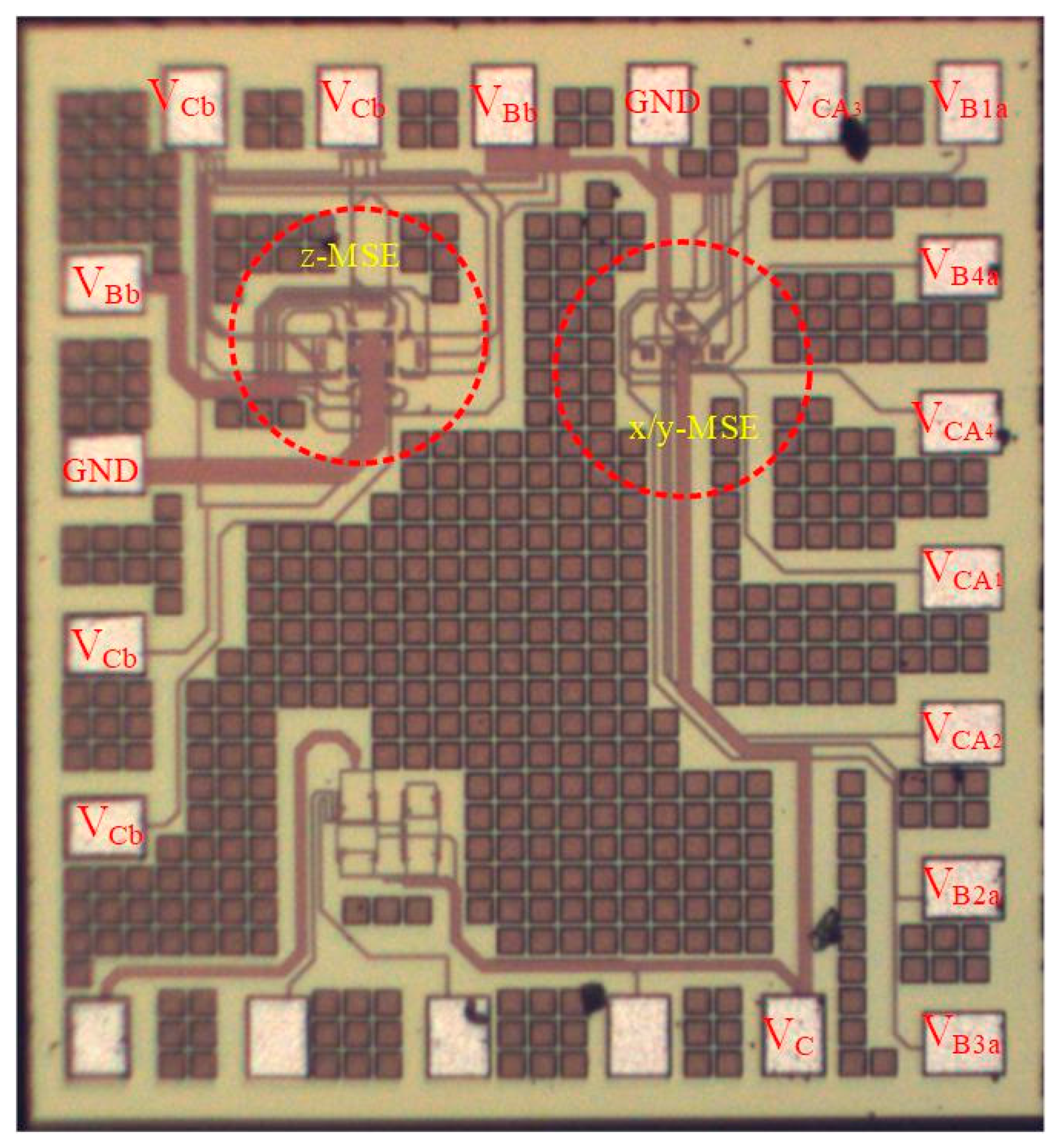
The three-axis micro MS includes an x/y-MSE and an z-MSE. The x/y-MSE is combined by an x-MSE and a y-MSE. The x-MSE and y-MSE are used to detect the MF in the x-direction and the y-direction, respectively. The z-MSE is employed to measure in the z-direction MF.
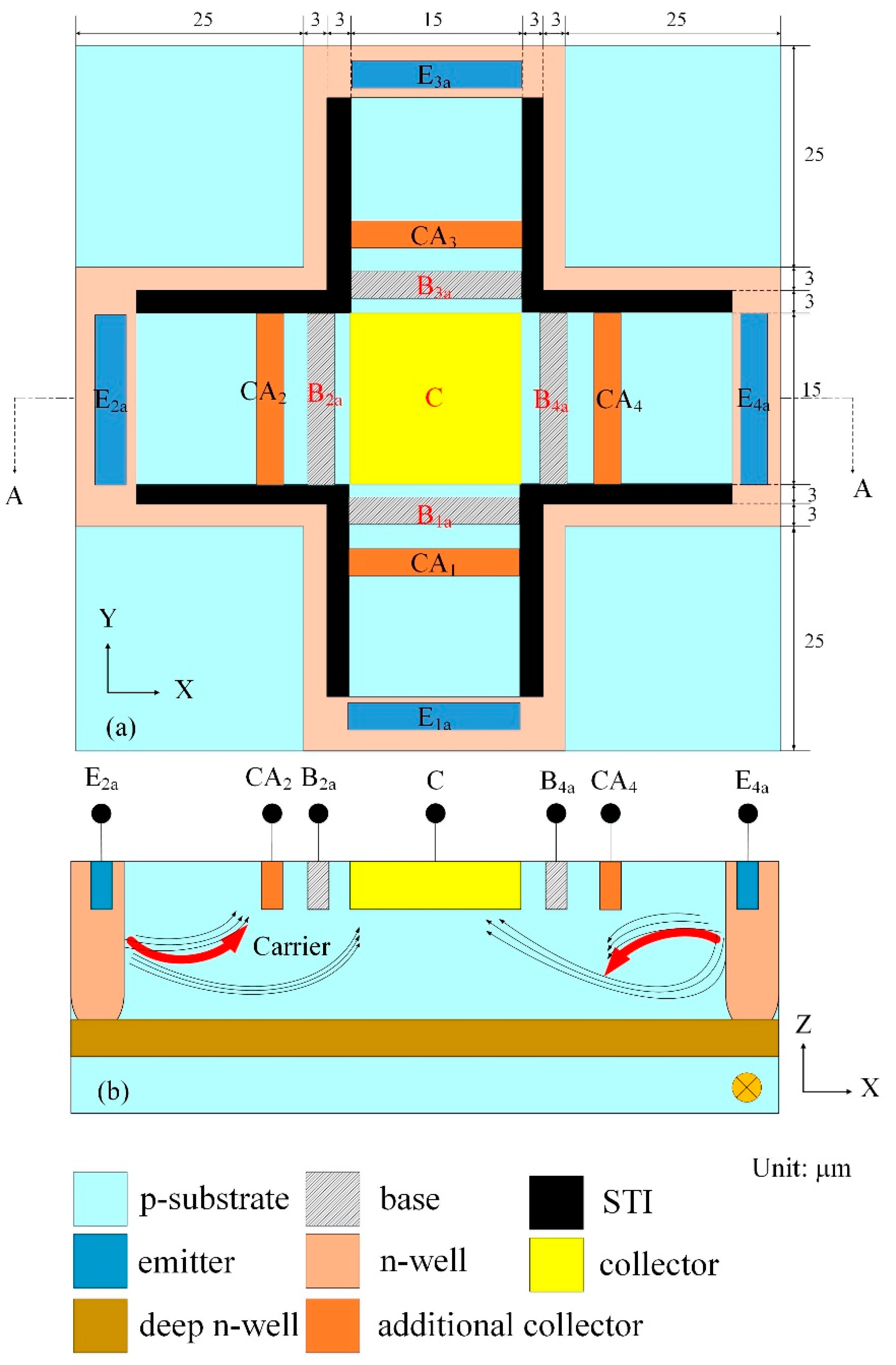
Figure 1a displays the x/y-MSE structure, where E
1a, E
2a, E
3a, and E
4a are emitters; B
1a, B
2a, B
3a and B
4a are bases; CA
1, CA
2, CA
3 and CA
4 are additional collectors; C is a collector; STI is shallow trench isolation. The STI is utilized to restrict the current moving direction and to decrease the current leakage. The x-MSE that is a magnetic transistor is constructed by the emitters E
1a and E
3a, the additional collectors CA
1 and CA
3, the bases B
1a and B
3a, and the collector C. The y-MSE is a symmetric structure with the x-MSE, and the y-MSE is composed of the emitters E
2a and E
4a, the additional collectors CA
2 and CA
4, the bases B
2a and B
4a, and the collector C.
The y-MSE cross-sectional view is illustrated in
Figure 1b. When the bias applies to the collector C, additional collectors (CA
2 and CA
4) and bases (B
2a and B
4a) and carriers move from the emitters (E
2a and E
4a) to the collector C, bases (B
2a and B
4a) and additional collectors (CA
2 and CA
4). There is an MF in the y-direction. The current and MF generate a Lorentz force that acts on carriers, resulting in carriers (on the right in
Figure 1b) are bended downward. Most carriers migrate to the collector C, such that the current of the additional collector CA
4 decreases. Opposite, carriers (on the left in
Figure 1b) are bended upward by the Lorentz force. Most carriers migrate to the additional collector CA
2, leading to an increase in the current of the additional collector CA
2. Therefore, when the y-direction MF applies to the x/y-MSE, the x/y-MSE generates a voltage difference between the additional collectors CA
2 and CA
4. The output voltage (Vo) of the MS is obtained by the voltage difference of the additional collectors CA
2 and CA
4 when applying a y-direction MF to the x/y-MSE.
As shown in
Figure 1b, the element structure of the x-MSE is similar to that of the y-MSE. The structure of the x-MSE, which consists of the emitters (E
1a and E
3a), the bases (B
1a and B
3a), the additional collectors (CA
1 and CA
3) and the collector C, is along the y-axis direction. When the bias applies to the collector C, additional collectors (CA
1 and CA
3) and bases (B
1a and B
3a) and carriers move from the emitters (E
1a and E
3a) to the collector C, bases (B
1a and B
3a) and additional collectors (CA
1 and CA
3). Suppose that there is an MF in the x-direction, then the current and the MF generate a Lorentz force that acts on carriers, such that carriers, which move from the emitter E
1a to the base B
1a and collector C, are bended downward. Most carriers migrate to the collector C, leading to a decrease in the current of the additional collector CA
1. Opposite, carriers that move from the emitter E
3a to the collector C and base B
3a are deflected upward by the Lorentz force. Most carriers migrate to the additional collector CA
3, such that the current of the additional collector CA
2 increases. Therefore, when the x-direction, MF applies to the x/y-MSE, the x/y-MSE produces a voltage difference between the additional collectors CA
1 and CA
3. The MS Vo is obtained by the voltage difference of the additional collectors CA
1 and CA
3 when applying the x-direction MF to the x/y-MSE.
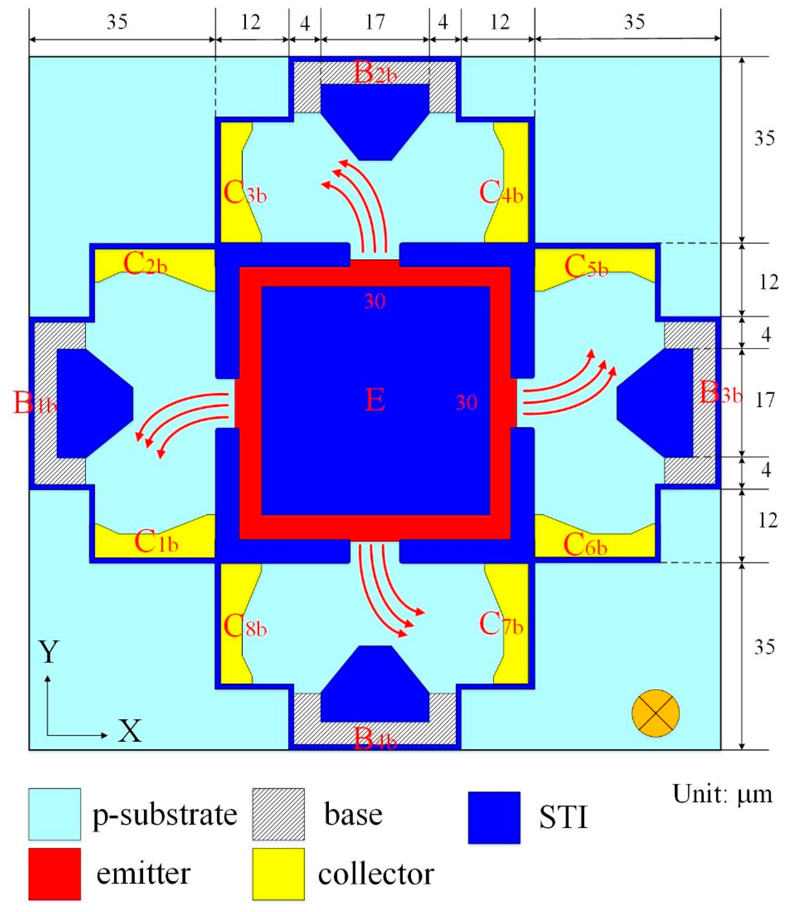
Figure 2 displays the z-MSE structure of the MS. The z-MSE is composed of one emitter E, four bases and eight collectors. The STI oxide is used to restrict the current moving direction and reduces the current leakage. When the bias applies to the bases and the collectors, carriers migrate from the emitter to the bases and collectors. There is an MF in the z-direction. The current and the MF produces a Lorentz force that acts on carriers, such that carriers are bended toward the collectors (C
1b, C
3b, C
5b and C
7b), resulting in the currents of the collectors (C
1b, C
3b, C
5b and C
7b) being higher than that of the collectors (C
2b, C
4b, C
6b and C
8b). A voltage difference is generated between the collectors. The Vo of the MS is obtained by the voltage differences in series when applying a z-direction MF to the z-MSE.
The performance of the x/y-MSE was simulated using the Sentaurus TCAD software. The x/y-MSE model (
Figure 1a) was set, and the Delaunay triangulation method was used to mesh the x/y-MSE model. The Poisson electron hole approach was employed to evaluate the electrical and MF coupling effect for the x/y-MSE. The Bank–Rose approach was employed to compute the distribution of carrier density for the x/y-MSE.
Figure 3 presents the simulated Vo for the MS in the x-direction MF, where V
B is the bias of the bases; V
C is the bias of the collector and V
CA is the bias of the additional collectors. In the evaluation, the collector C and additional collectors (CA
1, CA
2, CA
3 and CA
4), respectively, connected with a resistance of 1 kΩ. The bases bias was 2.5 V, and the collector bias was 5 V. The bias of the additional collectors was with different voltages of 0.5, 1, 1.5 and 2 V. The x/y-MSE was applied by the x-direction MF, and the x/y-MSE Vo was the voltage difference of the additional collector AC
1/AC
3. The evaluated results depicted that the MS Vo changed from −116 mV at −200 mT to 116 mV at 200 mT when V
B = 2.5 V, V
C = 5 V and V
CA =2 V. The slope of the curve (at V
B = 2.5 V, V
C = 5 V and V
CA =2 V) was 580 mV/T, so the evaluated sensitivity of the x/y-MSE was 580 mV/T at V
B = 2.5 V, V
C = 5 V and V
CA = 2 V in the x-direction MF.
The x/y-MSE was applied by the y-direction MF, and the Vo of the x/y-MSE was the voltage difference of the additional collector AC
2/AC
4.
Figure 4 shows the x/y-MSE Vo in the y-direction MF, where V
B is the bias of the bases; V
C is the bias of the collector and V
CA is bias of the additional collectors. The results presented that the MS Vo increased from −116 mV at −200 mT to 116 mV at 200 mT when V
B = 2.5 V, V
C = 5 V and V
CA = 2 V. The slope of the curve (at V
B = 2.5 V, V
C = 5 V and V
CA =2 V) was 580 mV/T, so the evaluated sensitivity for the x/y-MSE was 580 mV/T at V
B = 2.5 V, V
C = 5 V and V
CA = 2 V in the y-direction MF. The evaluated results of the x/y-MSE in the y-direction MF was the same with that in the x-direction MF because the x/y-MSE structure was a symmetric.
The performance of the z-MSE was simulated using the Sentaurus TCAD. The z-MSE model was established according to the structure in
Figure 2, and the z-MSE Vo was evaluated using the same simulation approach. In the simulation, the bases and collectors connected with a resistance of 1 kΩ, respectively. The bias of the bases was 1.5 V, the bias of the collectors was 5 V. The z-MSE was supplied by the z-direction MF, and the z-MSE Vo was computed by the Sentaurus TCAD.
Figure 5 shows the z-MSE Vo in the z-direction MF, where V
B is bias of the bases and V
C is bias of the collector. The evaluated results depicted that the z-MSE Vo changed from −26 mV at −200 mT to 26 mV at 200 mT when V
B = 1.5 V and V
C = 5 V. The slope of the curve at V
B = 2.5 V and V
C = 5 V was 130 mV/T, so the evaluated sensitivity of the z-MSE was 130 mV/T at V
B = 1.5 V and V
C = 5 V.
In order to characterize the MS cross-sensitivity, the cross-sensitivity of x/y-MSE and z-MSE were simulated using the Sentaurus TCAD with the same simulation approach. The bias of bases for the x/y-MSE was 2.5 V, and the bias of additional collectors for the x/y-MSE was 2 V. The bias of collector for the x/y-MSE was 5 V. At the same time, the bias of bases for the z-MSE was 1.5 V, and the bias of collectors for the z-MSE was 5 V. First, the Vo of the x/y-MSE and z-MSE was computed when applying an x-direction MF to the MS.
Figure 6 shows the evaluated output for the MS, where V
out(x,x) is the x-axis Vo for x/y-MSE in the x-direction MF; V
out(y,x) is the y-axis Vo for x/y-MSE Vo in the x-direction MF; V
out(z,x) is the z-MSE Vo in the x-direction MF. The results presented that the V
out(y,x) and V
out(z,x) values approximated to zero and the V
out(x,x) had a high response, so the MS cross-sensitivity in the x-direction MF was very small. Then, the Vo of the x/y-MSE and z-MSE was calculated when applying a y-direction MF to the MS.
Figure 7 shows the evaluated output for the MS, where V
out(x,y) is the x-axis Vo for x/y-MSE in the y-direction MF; V
out(y,y) is the y-axis Vo for x/y-MSE in the y-direction MF; V
out(z,y) is the z-MSE Vo in the y-direction MF. The results revealed that the V
out(x,y) and V
out(z,y) values approximated zero, and the V
out(y,y) had a high response. The MS cross-sensitivity in the y-direction MF was very small. Finally, the Vo of the x/y-MSE and z-MSE was simulated when applying a z-direction MF to the MS.
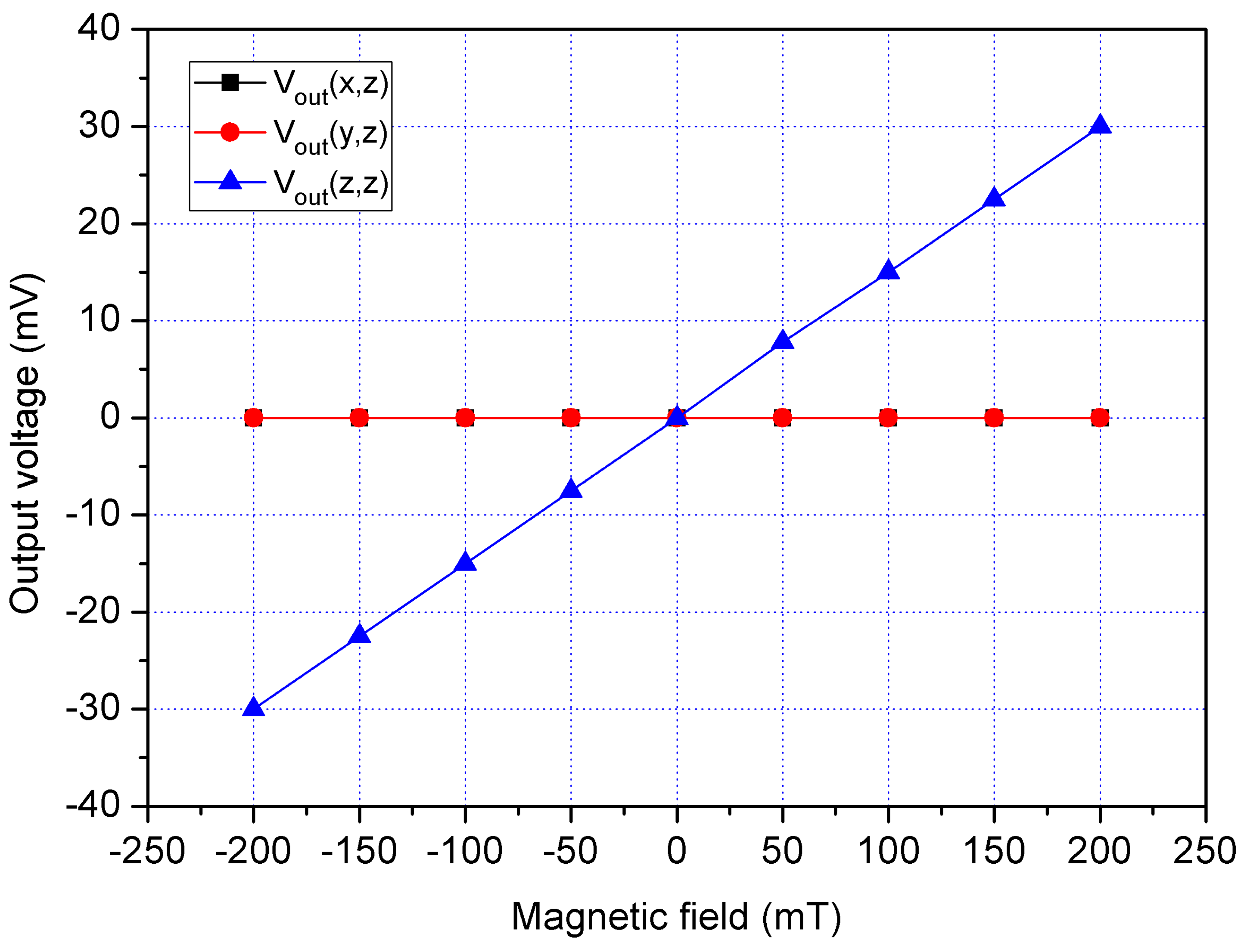
Figure 8 shows the evaluated output for the MS, where V
out(x,z) is the x-axis Vo for x/y-MSE in the z-direction MF; V
out(y,z) is the y-axis Vo for x/y-MSE in the z-direction MF; V
out(y,z) is the z-MSE Vo in the z-direction MF. The results depicted that the V
out(y,y) had a high response, and the V
out(x,y) and V
out(z,y) values approximated zero. The MS cross-sensitivity in the z-direction MF was very small.
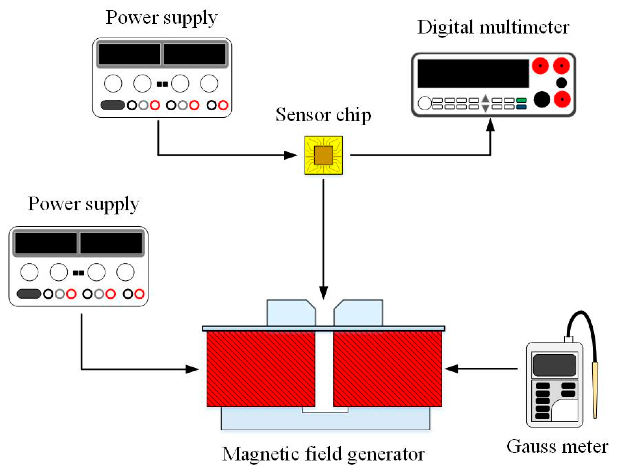
4. Results
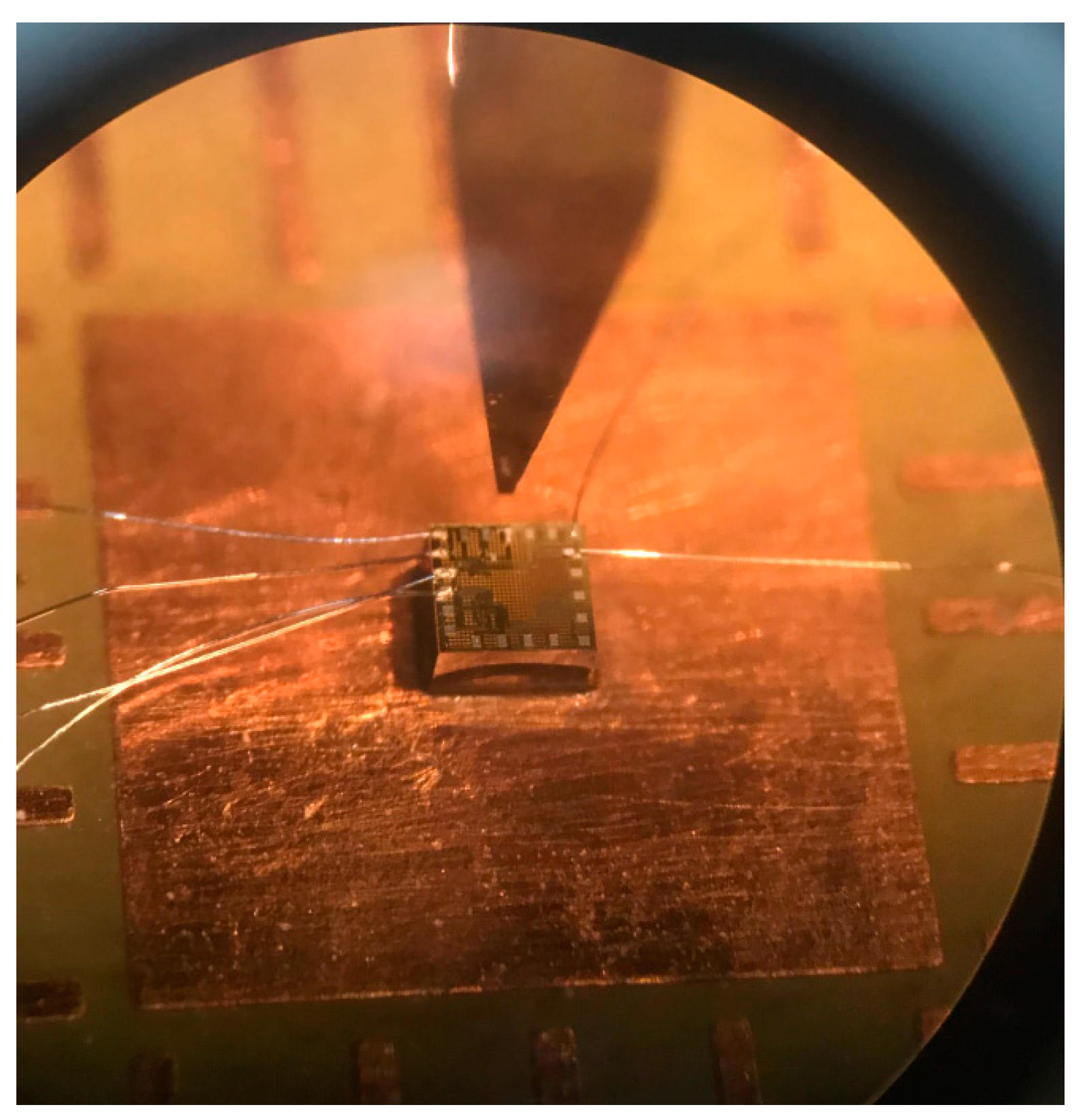
The three-axis MS was measured utilizing a digital multimeter, two power supplies, a Gauss meter and an MF generator.
Figure 11 demonstrates the setup for measuring the three-axis MS characteristic. The MS chip was placed in the MF generator. The power supply inputted power to the MF generator. The Gauss meter calibrated the MF magnitude that was produced by the MF generator. The MF generator supplied various MFs for the MS measurement. The power supply provided the bias for the MS. The digital multimeter measured the Vo of the three-axis MS.
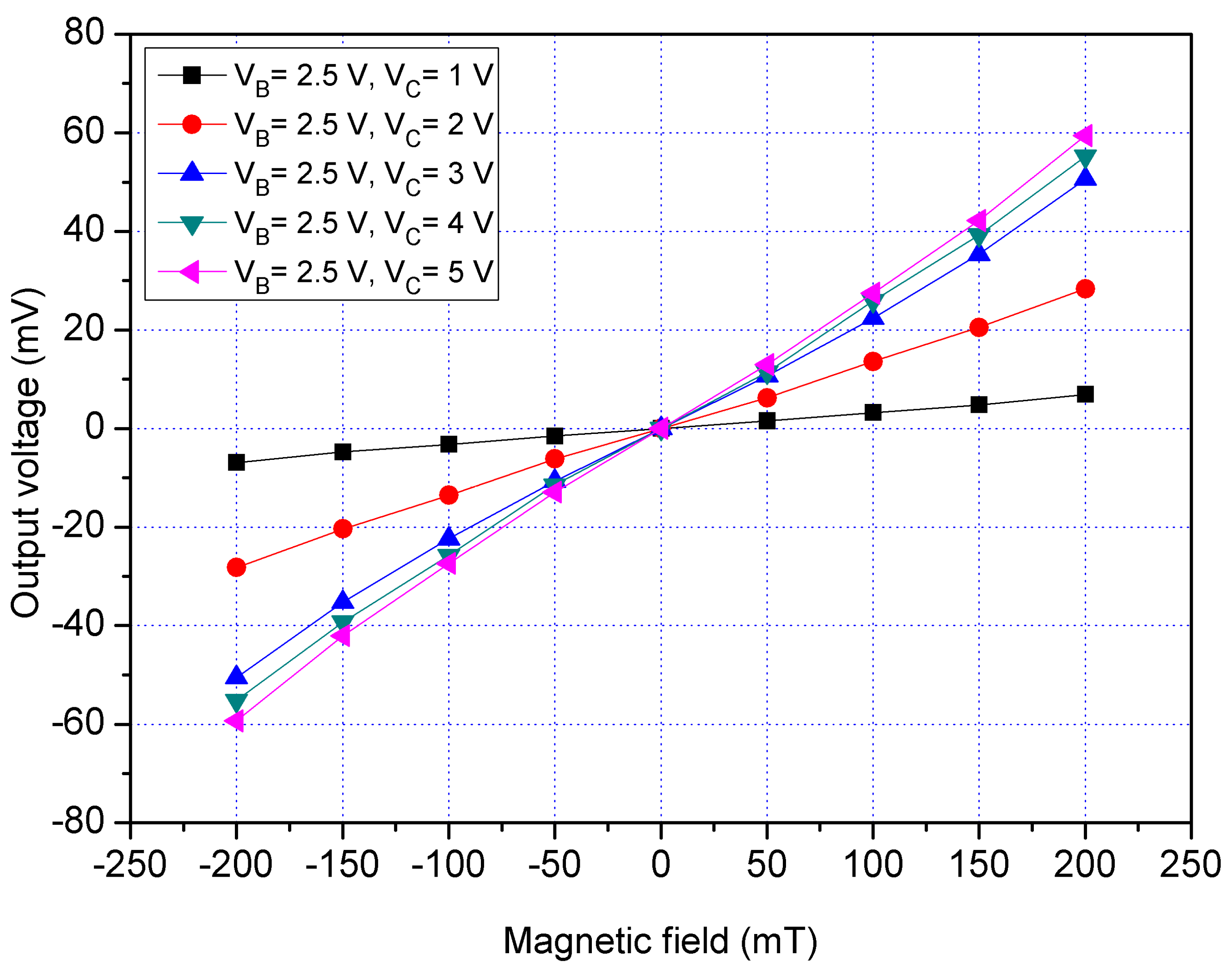
The x/y-MSE characteristic was tested in the x-direction MF. The MS chip (
Figure 11) was placed in the MF generator. An MF in the x-direction that was provided by the MF generator was applied to the x/y-MSE. A bias of 2.5 V was supplied to the bases of x/y-MSE. The additional collectors were without bias. The collector and each additional collector, respectively, was connected with a resistance of 1 kΩ. The different voltages including 1, 2, 3, 4 and 5 V were supplied to the collector of x/y-MSE. The x/y-MSE Vo that was the voltage difference between the addition collectors CA
1 and CA
3 was recorded by the digital multimeter. The tested results for the x/y-MSE without the additional collectors bias in the x-direction MF are shown in
Figure 12, where V
B is the bias of the bases and V
C is the bias of the collector. When V
B = 2.5 V and V
C = 1 V, the x/y-MSE Vo varied from −9.1 mV at −200 mT to 9.2 mV at 200 mT. When V
B = 2.5 V and V
C = 3 V, the x/y-MSE Vo increased from −50.5 mV at −200 mT to 50.6 mV at 200 mT. When V
B = 2.5 V and V
C = 5 V, the x/y-MSE Vo changed from −57.2 mV at −200 mT to 57.1 mV at 200 mT. The curve slope was 286 mV/T at V
B = 2.5 V and V
C = 5 V, so the x/y-MSE sensitivity was 286 mV/T at V
B = 2.5 V and V
C = 5 V in the x-direction MF.
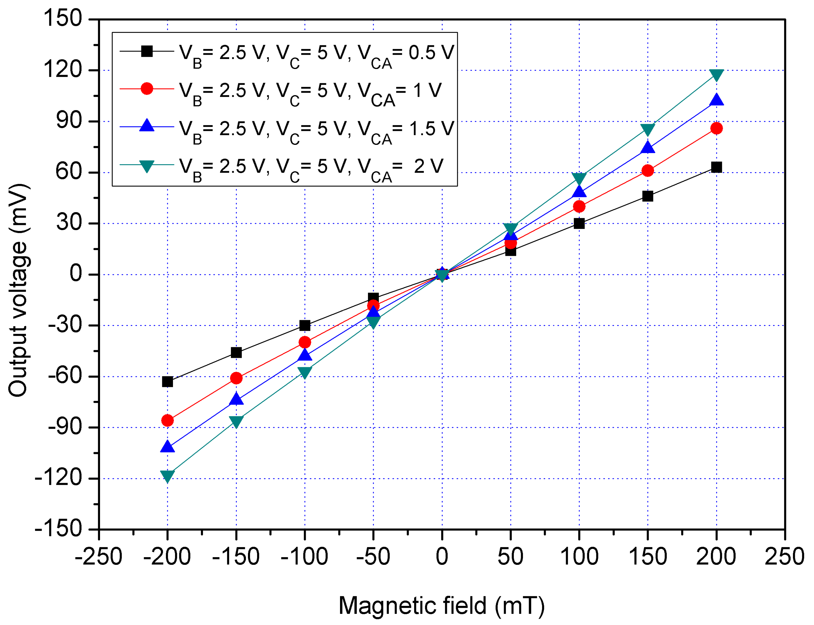
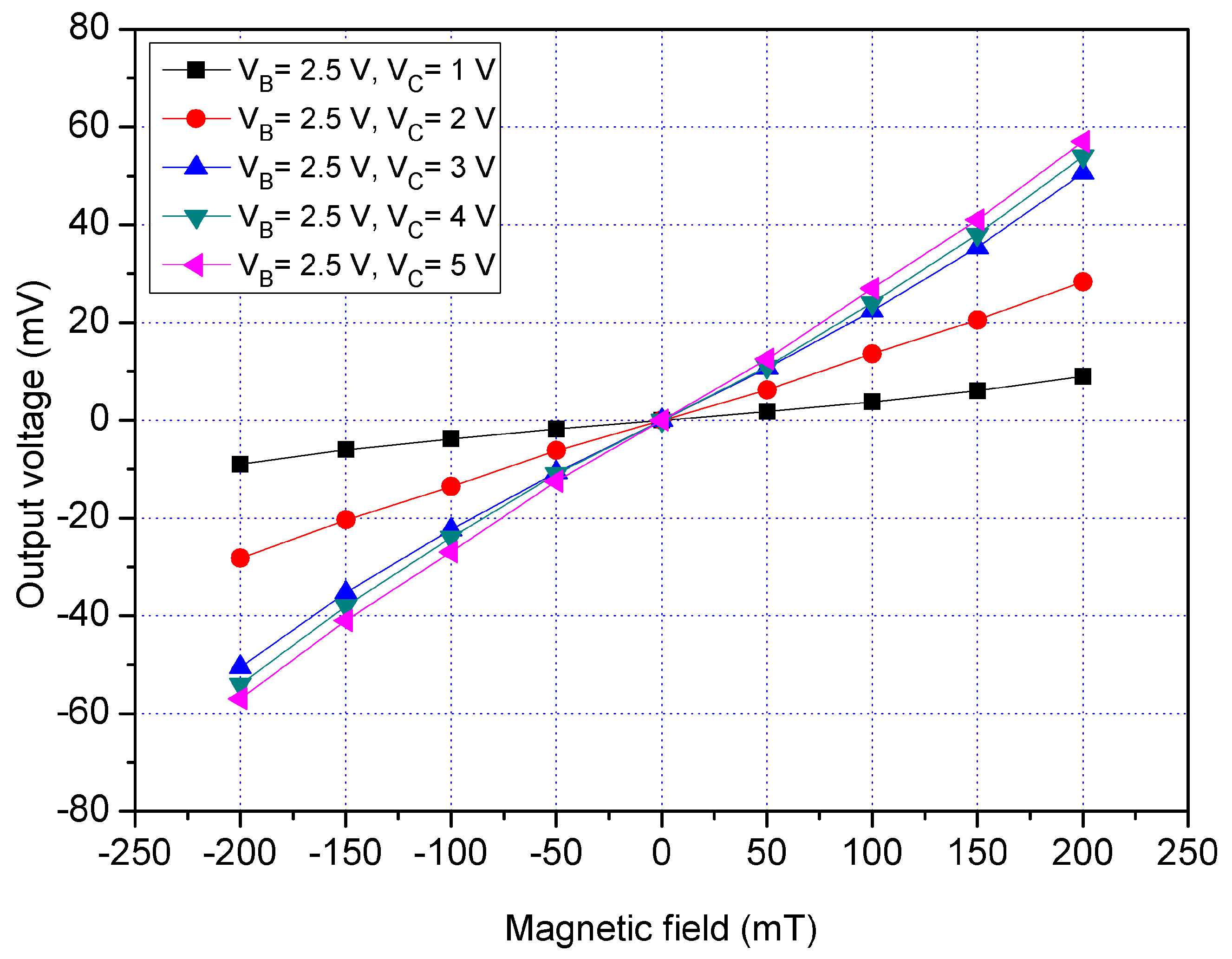
The x/y-MSE had the addition collectors that were used to increase the moving current and enhance the x/y-MSE sensitivity. To characterize the function of additional collectors, the x/y-MSE was measured under different biases of additional collectors. A bias of 2.5 V was provided to the bases of the x/y-MSE, and a bias of 5 V was applied to the collector of the x/y-MSE. The difference voltages that included 0.5, 1, 1.5 and 2 V were applied to the additional collectors of the x/y-MSE. The Vo of the x/y-MSE was recorded by a digital multimeter.
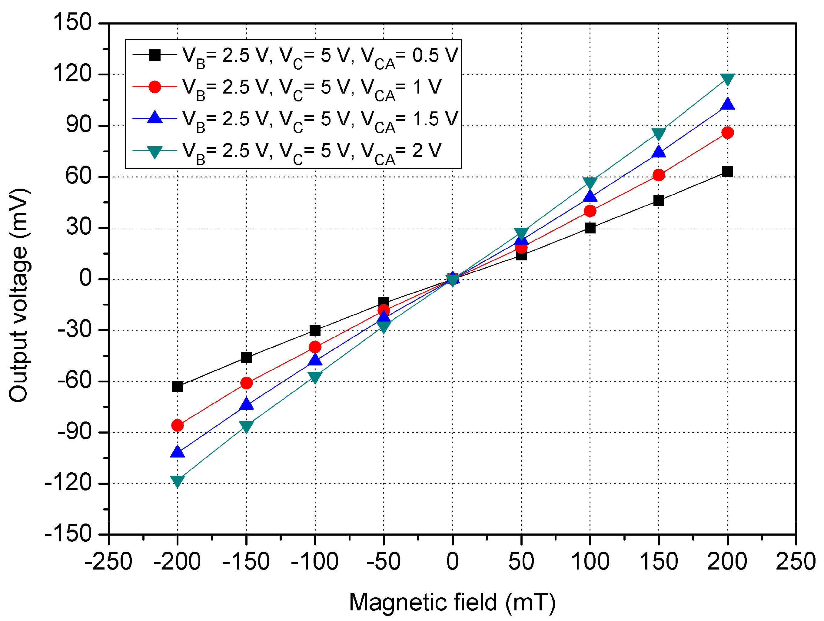
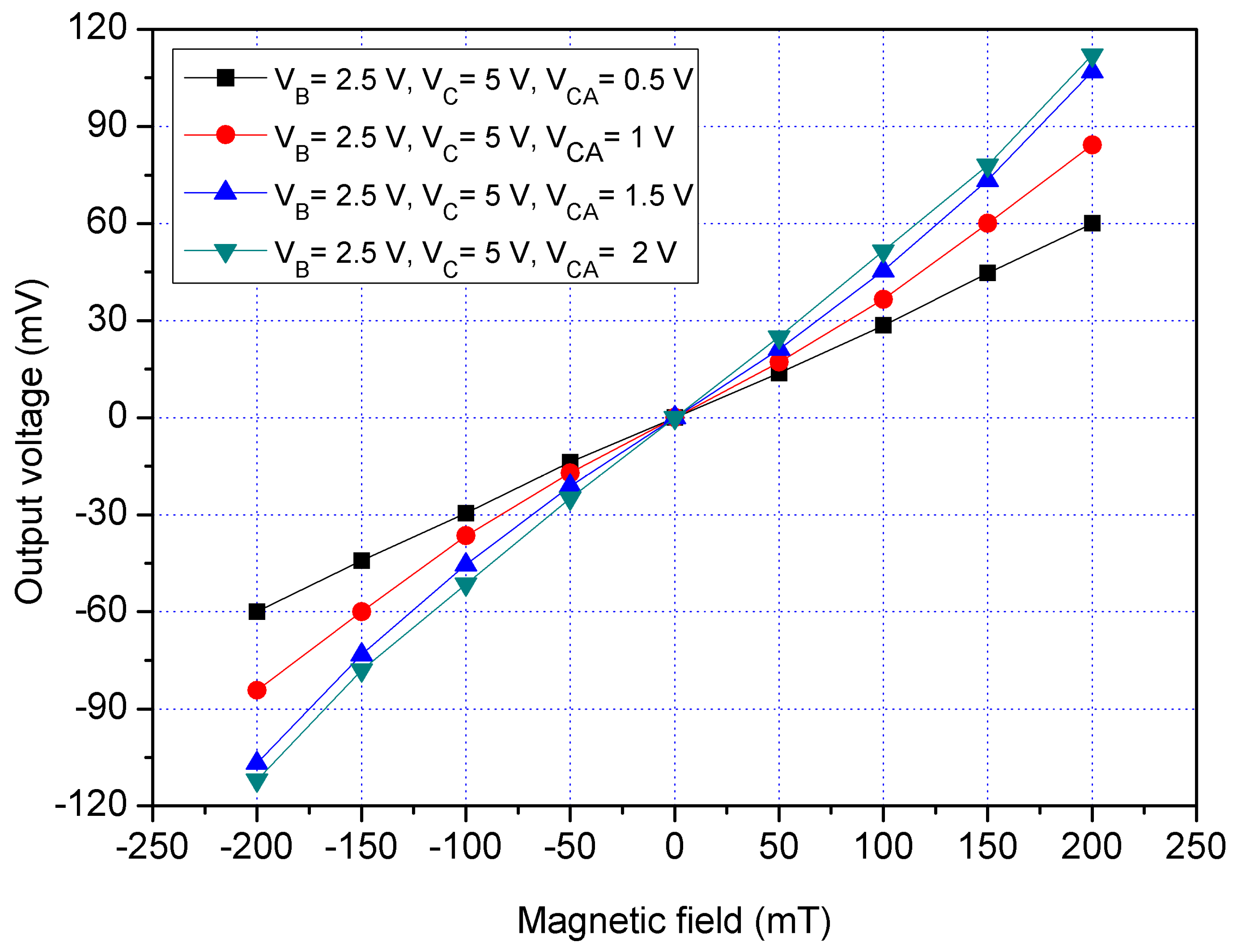
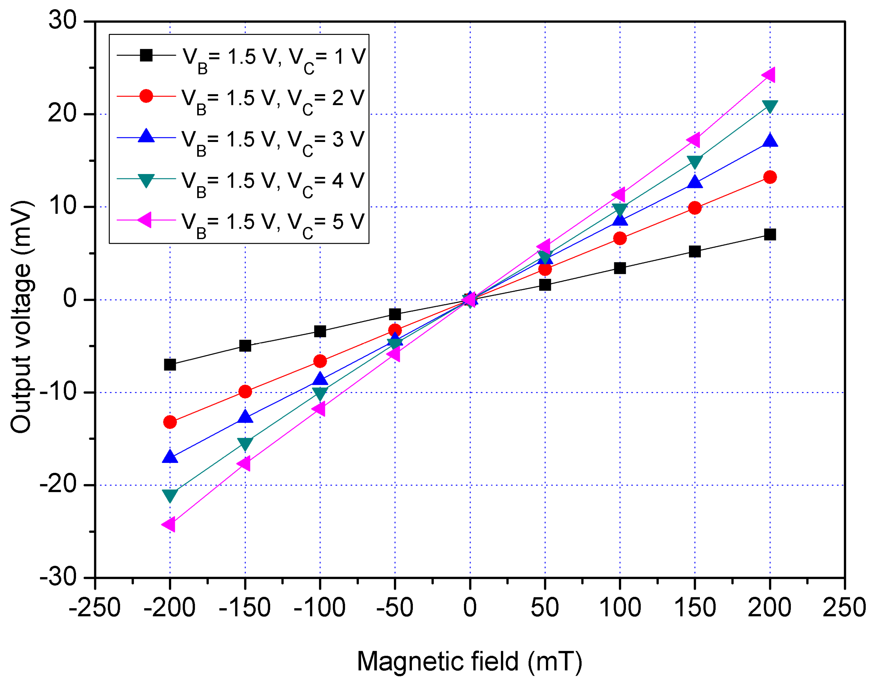
Figure 13 displays the measured Vo for the x/y-MSE with the additional collectors bias in the x-direction MF, where V
B is bias of the bases; V
C is bias of the collector and V
CA is bias of the additional collectors. When V
B = 2.5 V, V
C = 5 V and V
CA = 0.5 V, the x/y-MSE Vo varied from −60.3 mV at −200 mT to 60.2 mV at 200 mT. When V
B = 2.5 V, V
C = 5 V and V
CA = 1 V, the x/y-MSE Vo increased from −84.3 mV at −200 mT to 84.4 mV at 200 mT. When V
B = 2.5 V, V
C = 5 V and V
CA = 2 V, the x/y-MSE Vo changed from −112 mV at −200 mT to 112 mV at 200 mT. The linear regression method was used to fit the curve at V
B = 2.5 V, V
C = 5 V and V
CA = 2 V. The results showed that the regression line had a slope of 534 mV/T and a coefficient of determination R
2 = 0.9984, so the sensitivity of the x/y-MSE was 534 mV/T at V
B = 2.5 V, V
C = 5 V and V
CA = 2 V in the x-direction MF. The output linearity for the x-MSE was 99%. In a comparison of results in
Figure 12 and
Figure 13, the Vo of the x/y-MSE with the additional collectors bias exceeds that of the x/y-MSE without the additional collectors bias. In the x-direction MF, the sensitivity of the x/y-MSE (534 mV/T at V
B = 2.5 V, V
C = 5 V and V
CA=2 V) with the addition of collectors bias is higher than that of the x/y-MSE (286 mV/T at V
B = 2.5 V and V
C = 5 V) without the additional collectors bias.
The x/y-MSE characteristic was tested in the y-direction MF. As shown in
Figure 11, the MS chip was placed in the MF generator. An MF in the y-direction that was produced by the MF generator was supplied to the x/y-MSE. The collector and each additional collector connected with a resistance of 1 kΩ, respectively. A bias of 2.5 V was applied to the bases of the x/y-MSE. The additional collectors were without bias. The difference in voltages that had 1, 2, 3, 4 and 5 V were provided to the collector of the x/y-MSE. The Vo of the x/y-MSE that was the voltage difference between the addition collectors CA
2 and CA
4 and were recorded by the digital multimeter. The tested results for the x/y-MSE without the additional collectors bias in the y-direction MF is shown in
Figure 14, where V
B is the bias of the bases and V
C is the bias of the collector. When V
B = 2.5 V and V
C = 1 V, the x/y-MSE Vo varied from −8.9 mV at −200 mT to 9 mV at 200 mT. When V
B = 2.5 V and V
C = 3 V, the x/y-MSE Vo increased from −50.9 mV at −200 mT to 50.8 mV at 200 mT. When V
B = 2.5 V and V
C = 5 V, the x/y-MSE Vo changed from −56.9 mV at −200 mT to 56.8 mV at 200 mT. The slope of curve was 283 mV/T at V
B = 2.5 V and V
C = 5 V, so the sensitivity of the x/y-MSE was 283 mV/T at V
B = 2.5 V and V
C = 5 V in the y-direction MF.
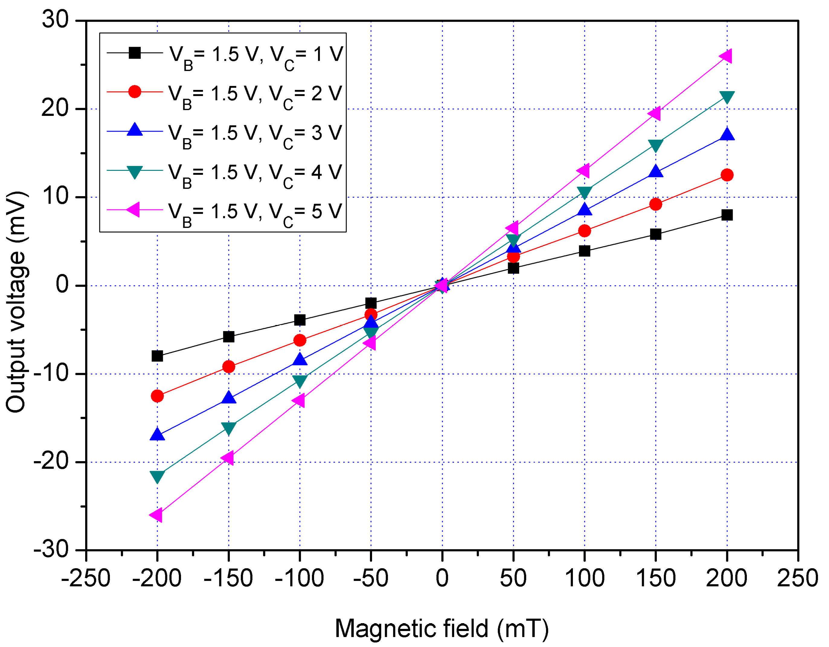
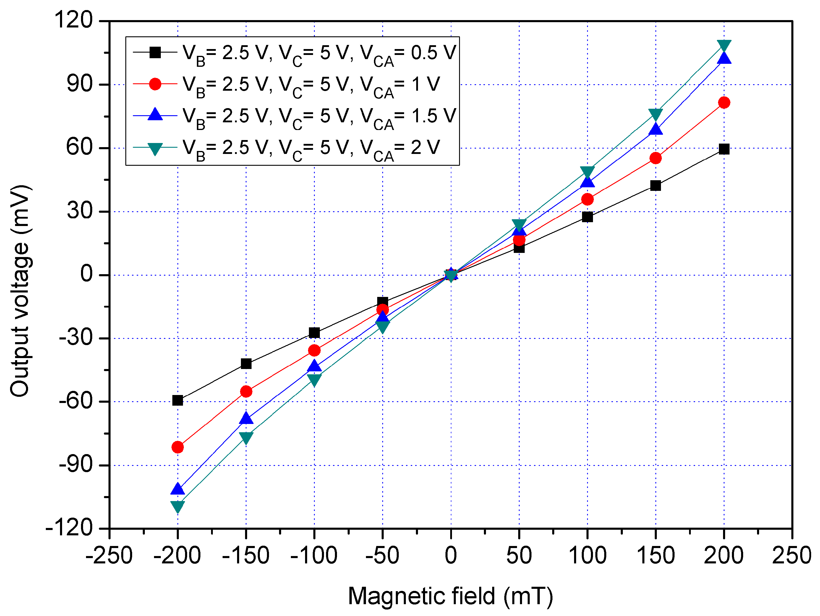
To understand the function of the additional collectors, the x/y-MSE was tested under the different biases of additional collectors. A bias of 2.5 V was applied to the bases of the x/y-MSE, and a bias of 5 V was supplied to the collector of the x/y-MSE. The different voltages that had 0.5, 1, 1.5 and 2 V were provided to the additional collectors of the x/y-MSE. The Vo of the x/y-MSE was measured by the digital multimeter.
Figure 15 displays the measured Vo for the x/y-MSE with the additional collectors bias in the y-direction MF, where V
B is the bias of the bases; V
C is the bias of the collector and V
CA is the bias of the additional collectors. When V
B = 2.5 V, V
C = 5 V and V
CA = 0.5 V, the x/y-MSE Vo varied from −59.5 mV at −200 mT to 59.6 mV at 200 mT. When V
B = 2.5 V, V
C = 5 V and V
CA = 1 V, the x/y-MSE Vo increased from −83.6 mV at −200 mT to 83.5 mV at 200 mT. When V
B = 2.5 V, V
C = 5 V and V
CA = 2 V, the x/y-MSE Vo changed from −111.5 mV at −200 mT to 111.5 mV at 200 mT. The linear regression method was employed to fit the curve at V
B = 2.5 V, V
C = 5 V and V
CA = 2 V. The results depicted that the regression line had a slope of 525 mV/T and a coefficient of determination R
2 = 0.9982, so the sensitivity of the x/y-MSE was 525 mV/T at V
B = 2.5 V, V
C = 5 V and V
CA = 2 V in the y-direction MF. The output linearity for the y-MSE was 99%. A comparison of results in
Figure 14 and
Figure 15, the Vo of the x/y-MSE with the additional collectors bias exceeds that of the x/y-MSE without the additional collectors bias. In the y-direction MF, the sensitivity of the x/y-MSE (525 mV/T at V
B = 2.5 V, V
C = 5 V and V
CA = 2 V) with the addition collector bias exceeds that of the x/y-MSE (283 mV/T at V
B = 2.5 V and V
C =5 V) without the additional collectors bias.
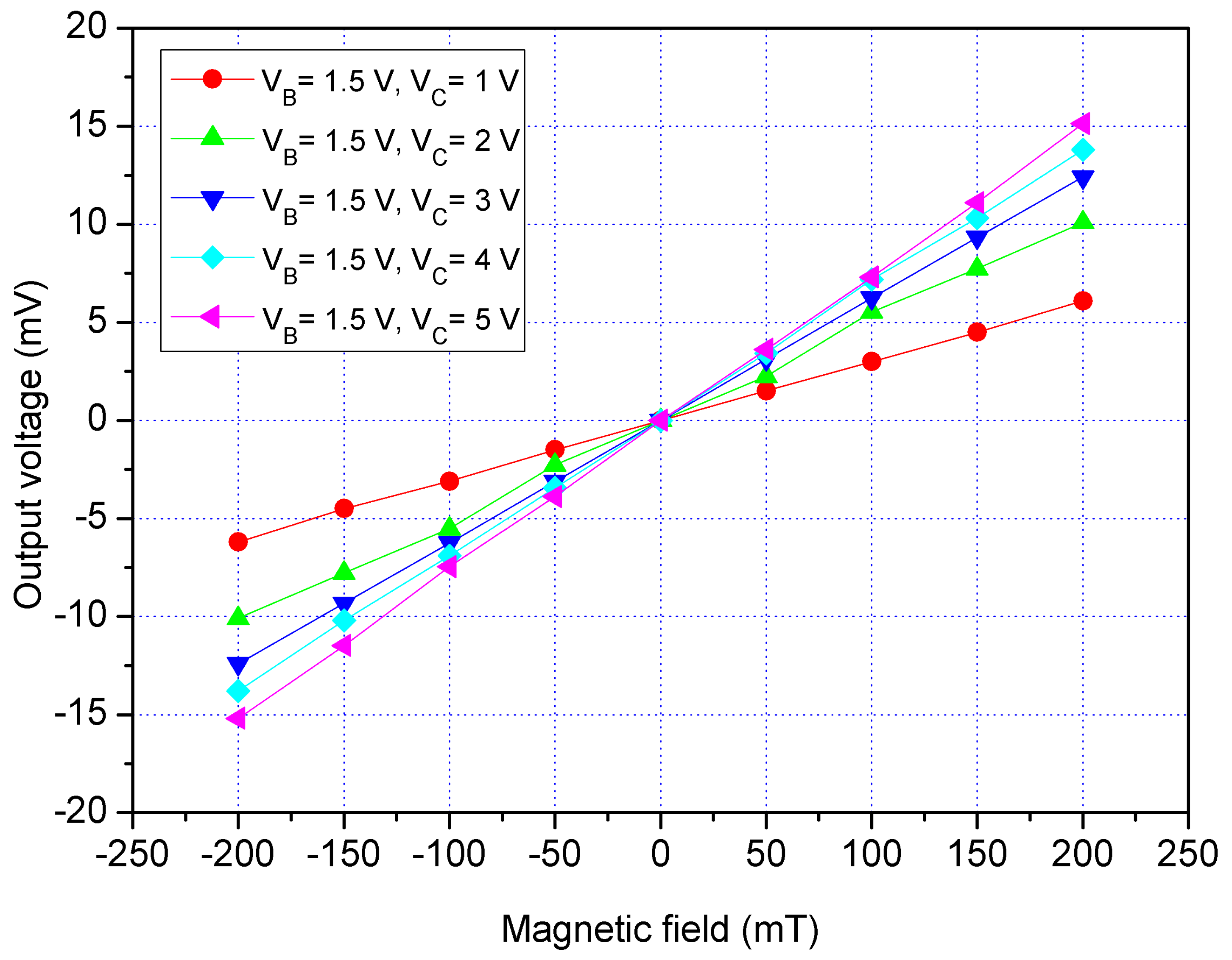
The z-MSE characteristic was tested in the z-direction MF. The MF generator produced a z-direction MF that applied to the z-MSE. The power supply provided a bias of 1.2 V to the bases of the z-MSE. The difference voltages that had 1, 2, 3, 4 and 5 V were applied to the collectors of the z-MSE. The bases and collectors were connected with a resistance of 1 kΩ, respectively. The Vo of the z-MSE was detected by the digital multimeter.
Figure 16 displays the measured Vo for the z-MSE at V
B = 1.2 V in the z-direction MF, where V
B is bias of the bases and V
C is bias of the collectors. When V
B = 1.2 V and V
C = 1 V, the z-MSE Vo increased from −6.2 mV at −200 mT to 6.1 mV at 200 mT. When V
B = 1.2 V and V
C = 3 V, the z-MSE Vo changed from −12.4 mV at −200 mT to 12.4 mV at 200 mT. When V
B = 1.2 V and V
C = 5 V, the z-MSE Vo varied from −15.2 mV at −200 mT to 15.1 mV at 200 mT. The slope of curve was 75 mV/T at V
B = 1.2 V and V
C = 5 V, so the sensitivity of the x/y-MSE was 75 mV/mT at V
B = 1.2 V and V
C = 5 V in the z-direction MF. To characterize the influence of the bases voltage for the z-MSE, the bias of the bases was increased to 1.5 V. The difference voltages that included 1, 2, 3, 4 and 5 V were supplied to the collectors of the z-MSE.
Figure 17 shows the measured Vo for the z-MSE at V
B = 1.5 V in the z-direction MF, where V
B is the bias of the bases and V
C is the bias of the collectors. When V
B = 1.5 V and V
C = 1 V, the z-MSE Vo changed from −7.5 mV at −200 mT to 7.6 mT at 200 mV. When V
B = 1.5 V and V
C = 3 V, the z-MSE Vo varied from −17.3 mV at −200 mT to 17.3 mT at 200 mV. When V
B = 1.5 V and V
C = 5 V, the z-MSE Vo increased from −24.2 mV at −200 mT to 24.1 mV at 200 mT. The linear regression method was used to fit the curve at V
B = 1.5 V and V
C = 5 V. The results showed that the regression line had a slope of 119 mV/T and a coefficient of determination R
2 = 0.9995, so the sensitivity of the z-MSE was 119 mV/T at V
B = 1.5 V and V
C = 5 V in the z-direction MF. The output linearity for the z-MSE was 99%. A comparison of results in
Figure 16 and
Figure 17, the Vo of the z-MSE at V
B = 1.5 V exceeds that of the z-MSE at V
B = 1.2 V. In the z-direction MF, and the sensitivity of the z-MSE increases from 75 mV/T at V
B = 1.2 V and V
C = 5 V to 119 mV/T at V
B = 1.5 V and V
C = 5 V.
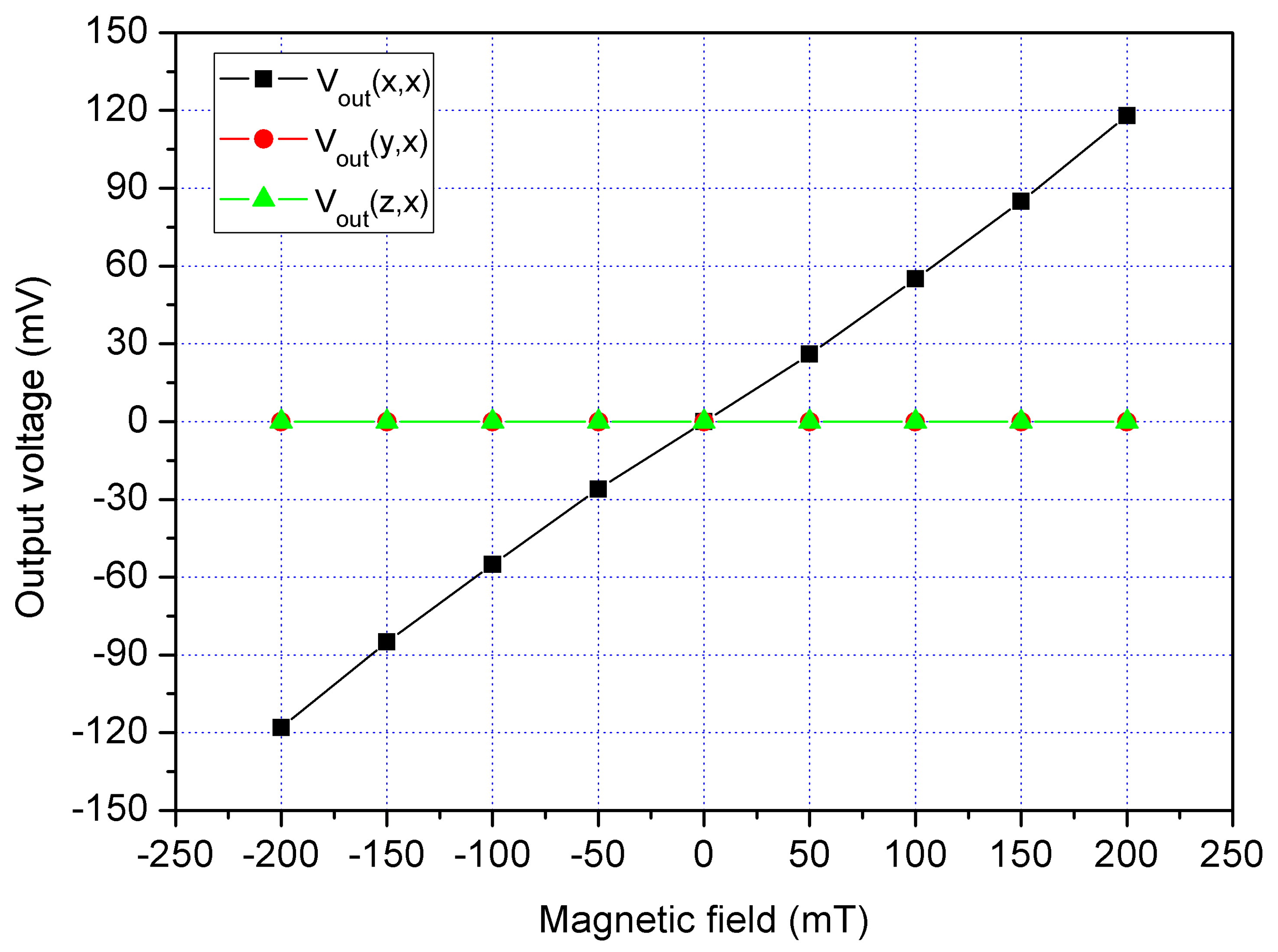
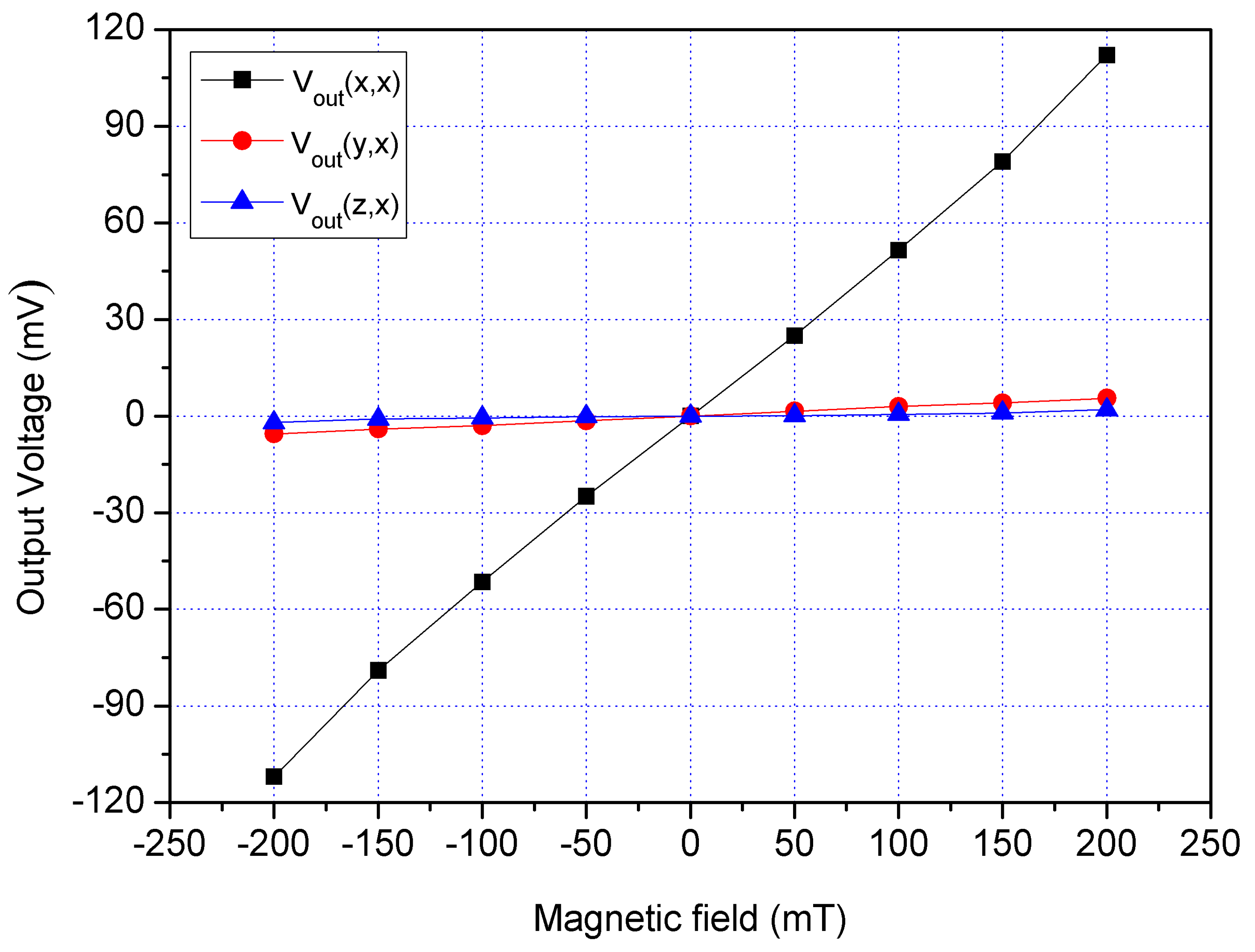
An excellent three-axis MS must have a low cross-sensitivity. The cross-sensitivity of the MS was investigated. First, an x-direction MF was applied to the MS. A bias of 2.5 V was supplied to the bases of x/y-MSE. A bias of 5 V was provided to the collector of x/y-MSE, and a bias of 2 V was applied to the additional collectors of x/y-MSE. At the same time, a bias of 1.5 was supplied to the bases of z-MSE, and a bias of 5 V was provided to the collectors of z-MSE. The digital multimeter measured the Vo of the x/y-MSE and z-MSE.
Figure 18 displays three-axis Vo for the MS in the x-direction magnetic, where V
out(x,x) is the x-axis Vo for the x/y-MSE in the x-direction MF; V
out(y,x) is the y-axis Vo for the x/y-MSE in the x-direction MF and V
out(z,x) is the z-MSE Vo in the x-direction MF. The V
out(y,x) and V
out(z,x) values in
Figure 18 are very small. The slope of the curve V
out(y,x) was 25.4 mV/T, and the slope of the curve V
out(z,x) was 11.2 mV/T. In the x-direction MF, the MS had a cross-sensitivity of 25.4 mV/T (y-axis output) and a cross-sensitivity of 11.2 mV/T (z-axis output). The MS sensitivity in the x-direction MF was 534 mV/T, so the MS cross-sensitivity in x-direction MF was less than 4.8%.
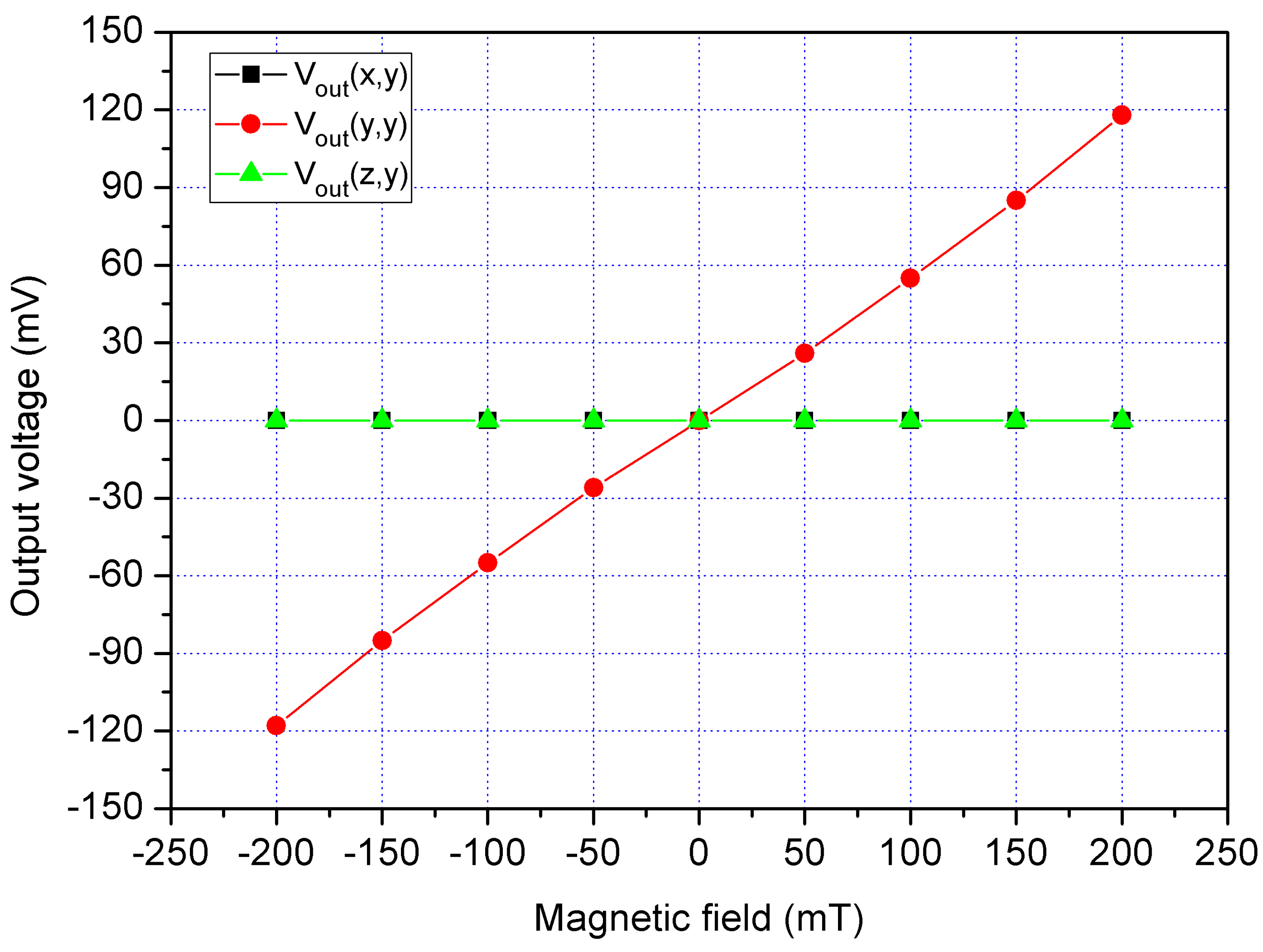
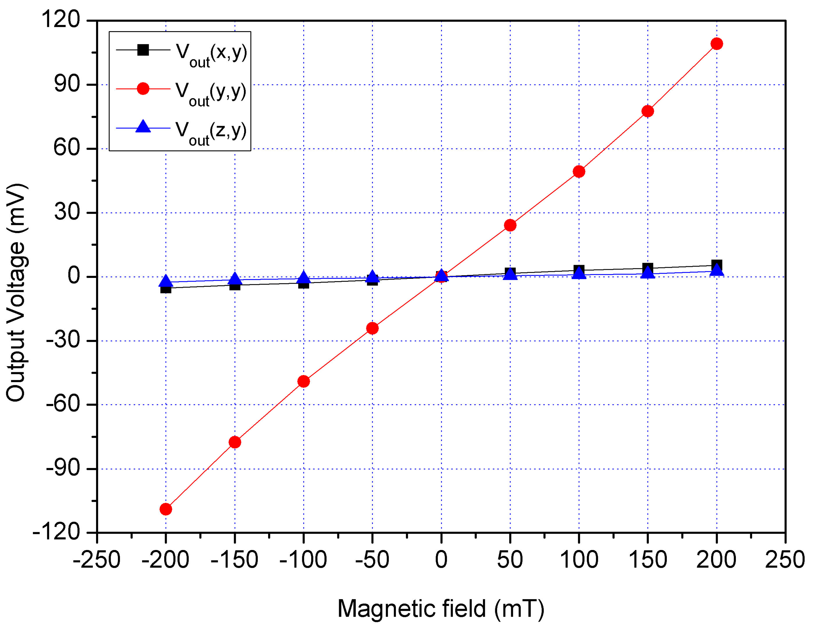
A y-direction MF was provided to the MS. A bias of 2.5 V was provided to the bases of x/y-MSE. A bias of 5 V was supplied to the collector of x/y-MSE, and a bias of 2 V was applied to the additional collectors of x/y-MSE. At the same time, a bias of 1.5 was applied to the bases of z-MSE, and a bias of 5 V was supplied to the collectors of z-MSE. The digital multimeter recorded the Vo of the x/y-MSE and z-MSE.
Figure 19 displays three-axis Vo for the MS in the y-direction magnetic, where V
out(x,y) is the x-axis Vo for the x/y-MSE in the y-direction MF; V
out(y,y) is the y-axis Vo for the x/y-MSE in the y-direction MF and V
out(z,y) is the z-MSE Vo in the y-direction MF. The V
out(x,y) and V
out(z,y) values in
Figure 19 are very low. The slope of the curve V
out(x,y) was 24.5 mV/T, and the slope of the curve V
out(z,y) was 12 mV/T. In the y-direction MF, the MS had a cross-sensitivity of 24.5 mV/T (x-axis output) and a cross-sensitivity of 12 mV/T (z-axis output). The MS sensitivity in the y-direction MF was 525 mV/T, so the MS cross-sensitivity in y-direction MF was less than 4.7%.
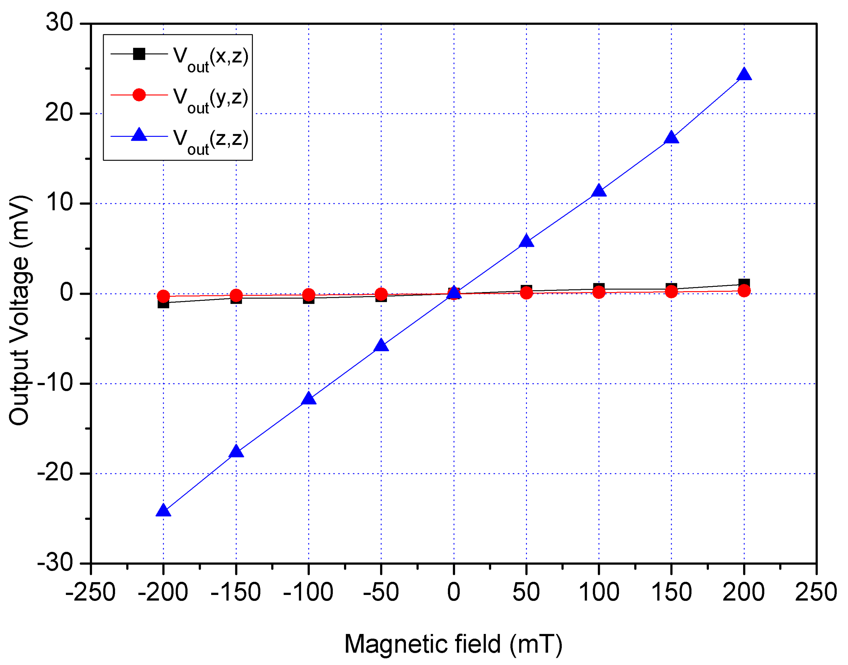
A z-direction MF was supplied to the MS. A bias of 2.5 V was applied to the bases of x/y-MSE. A bias of 5 V was provided to the collector of x/y-MSE, and a bias of 2 V was supplied to the additional collectors of x/y-MSE. At the same time, a bias of 1.5 was supplied to the bases of z-MSE, and a bias of 5 V was applied to the collectors of z-MSE. The digital multimeter detected the Vo of the x/y-MSE and z-MSE.
Figure 20 displays three-axis Vo for the MS in the z-direction magnetic, where V
out(x,z) is the x-axis Vo for the x/y-MSE in the z-direction MF; V
out(y,z) is the y-axis Vo for the x/y-MSE in the z-direction MF and V
out(z,z) is the z-MSE Vo in the z-direction MF. The V
out(x,z) and V
out(y,z) values in
Figure 20 are very small. The slope of the curve V
out(x,z) was 3.4 mV/T, and the slope of the curve V
out(y,z) was 3.2 mV/T. In the z-direction MF, the MS had a cross-sensitivity of 3.4 mV/T (x-axis output) and a cross-sensitivity of 3.2 mV/T (y-axis output). The MS sensitivity in the z-direction MF was 119 mV/T, so the MS cross-sensitivity in z-direction MF was less than 2.9%.
Table 2 summarizes the performances of the magnetic sensor. The area of the x/y-MSE is 80 × 80 μm
2, and the area of z-MSE is 120 × 120 μm
2. The measurement range of magnetic field for the x-MSE, y-MSE and z-MSE is ±200 mT. The sensitivity of the x-MSE is 534 mV/T, and the sensitivity of the y-MSE is 525 mV/T. The sensitivity for the z-MSE is 119 mV/T. The cross-sensitivity of the x-MSE is less than 4.8%. The cross-sensitivity for the y-MSE is less than 4.7%, and the cross-sensitivity for the z-MSE is less than 2.9%. The output linearity for the x-MSE (coefficient of determination R
2 = 0.9984), y-MSE (R
2 = 0.9982) and z-MSE (R
2 = 0.9995) is 99%. The power consumption of the x/y-MSE is 6 mW, and the power consumption of the z-MSE is 4 mW.
These micro magnetic sensors, proposed by Niekiel [
9], Okada [
11], Nejad [
13], Bahreyni [
14], were magnetic-resonant types that had a high sensitivity. The magnetic-resonant magnetic sensors required suspension structures and a high-actuated voltage to produce actuation and sensing, so the sensors had the disadvantages of a complicated fabrication, high-actuated voltage, high power consumption, and easy interference by environmental vibration. In this work, the micro magnetic sensor was without a suspension structure and was fabricated using the commercial CMOS process, so the sensor had the advantages of a low power consumption, easy fabrication and easy mass-production. Tseng [
15] developed a one-axis micro-magnetic sensor using the CMOS process, and the sensor was a magnetic transistor type. The sensitivity of the magnetic sensor was 354 mV/T. Sileo [
16] fabricated a Hall magnetic sensor, and its sensitivity was 0.03 V/T. Zhao [
17] proposed a three-axis micro magnetic sensor manufactured using the MEMS technology. The magnetic sensor was composed of four magnetic transistors and a Hall element. The x-axis, y-axis and z-axis sensitivity for the magnetic sensor were 77.5 mV/T, 78.6 mV/T and 77.4 mV/T, respectively. In this work, the magnetic sensor was a magnetic transistor type, and the sensitivity of the sensor exceeded that of Tseng [
15], Sileo [
16] and Zhao [
17].


