Abstract
A 24 GHz high linear, high-gain up-conversion mixer is realized for fifth-generation (5G) applications in the 65 nm CMOS process. The mixer’s linearity is increased by applying an Improved Derivative Super-Position (I-DS) technique cascaded between the mixer’s transconductance and switching stage. The high gain and stability of amplifiers in the transconductance stage of the mixer are achieved using novel tunable capacitive cross-coupled common source (TCC-CS) transistors. Using the I-DS, the third-order non-linear coefficient of current is closed to zero, enhancing the linearity. Additionally, a TCC-CS, which is realized by varactors, neutralizes the gate-to-drain parasitic capacitance (Cgd) of transistors in the transconductance stage of the mixer and contributes to the improvement of the gain and stability of the mixer. The measured 1 dB compression point OP1dB of the designed mixer is 4.1 dBm and IP1dB is 0.67 dBm at 24 GHz. The conversion gain of 4.1 dB at 24 GHz and 3.2 ± 0.9 dB, from 20 to 30 GHz is achieved in the designed mixer. Furthermore, a noise figure of 3.8 dB is noted at 24 GHz. The power consumption of the mixer is 4.9 mW at 1.2 V, while the chip area of the designed mixer is 0.4 mm.
1. Introduction
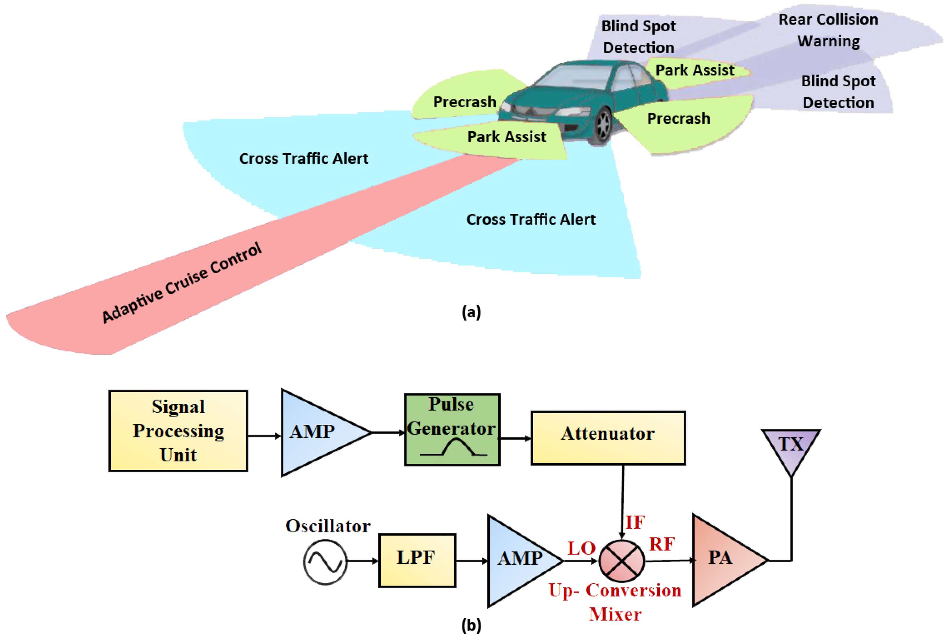
In recent studies, the demand for 5G communication systems was shown to have enormously increased. There are many 5G mobile communication devices available; some of them are wireless broadband internet, cellular phones, etc. Low power, low voltage and highly linear RF circuits attract considerable attention in regard to prolonging the battery life of communication systems. The 5G system is becoming a necessity in wireless communication [,]. Existing technologies, including LTE and 4G mobile communications, cannot satisfy the increasing demands for a fast data rate, low latency and larger capacity. The 5G system is 1000 times faster than 4G technology. Furthermore, 5G accumulates high data traffic capacity. Many advanced communication applications require a high capacity, high data rate communication system, and the 5G technologies fulfill these requirements. A frequency band from 20 GHz to 30 GHz has been relevant in 5G radar applications []. Vehicular Radar systems can give useful insight into the other millimeter-wave applications. Additionally, in the automotive sector, radars are widely employed for the development of cars, which offer the basis for a secure and intelligent transport system []. The 5G frequency spectrum gained a great deal of attention because of its prospective usage of automobile vehicles for radar applications []. Nowadays, automotive radar is regarded as one of 5G technology’s most important vertical markets. Thus, in [], the author also describes a 5G transceiver radar application (24 GHz) that achieves a high data rate and wide bandwidth. The radar applications in automobile vehicles and radar transmitter design are shown in Figure 1a,b, respectively.
Figure 1.
(a) Automobile radar application, (b) radar transmitter design.
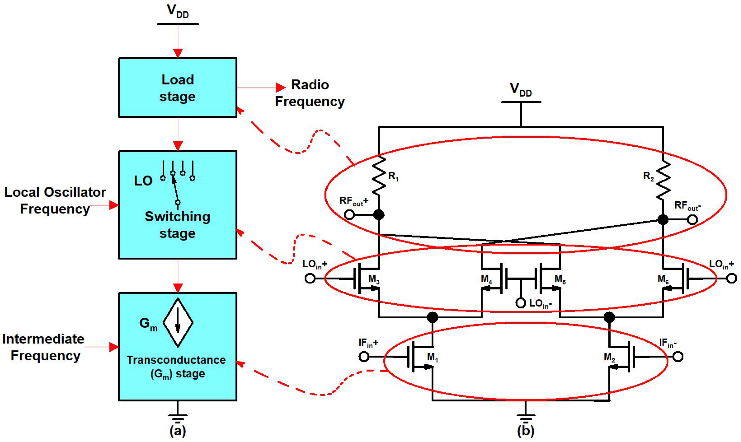
High integration, low power, low noise, and high linearity are the main design requirements in the 5G transmitter design. An up-conversion mixer is the main circuit block in a 5G radar transmitter design. Designing a highly linear, high-gain up-conversion mixer is a fundamental challenge in transmitter design. A highly linear, high-gain up-conversion mixer is compulsory to overcome the transmitter linearity limitation. Linearity is an essential characteristic of an up-conversion mixer because a transmitter with a mixer with low linear output requires a buffer amplifier to drive a power amplifier that degrades the linearity. So, a linear up-conversion mixer with a high-output 1 dB compression point (OP1dB) benefits the transmitter design. The block diagram and schematic of the conventional mixer are shown in Figure 2a,b, respectively.
Figure 2.
(a) Block diagram, (b) schematic of the conventional of mixer.
Related Literature Survey
In general, mixers are often categorized as passive and active mixers. Passive mixers can be used to generate an intermediate frequency (IF) for a local oscillator (LO) driving signal by using passive switches. Passive mixers could attenuate the signal. On the other hand, active mixers offer a positive conversion gain (CG), while passive mixers do not []. However, passive mixers are simple. They have zero power consumption, are highly linear, have good NF, but they require a high LO power. Active mixers offer excellent CGs, good port isolation, and minimum NF and LO power, unlike passive mixers. When analyzing all these facts, active mixers are preferred over passive mixers.
Recently, many active CMOS up/down mixers [] were reported with different topologies that enhanced the linearity and gain performances. Zumbahlen et al. [] proposed a circuit with a minimum amount of noise and strong linearity, while Siddiqi et al. [] described the mixer design as having a minimal NF but inadequate CG and linearity. Additionally, in [], the proposed mixers have minimal power consumption and high linearity; however, these mixers are often employed at the expense of port isolation, and the shortcoming is that they require a high LO power. In [], the author designed the most popular Gilbert mixer, showing high isolation. Another previous study [] described a mixer with high performance in terms of CG and NF but at the expense of linearity. In [,], the LO and radio frequency (RF) signals were applied at the drain and gate terminals of the transistor, but these mixers suffered with poor linearity. In [,], to enhance the linearity, a CMOS mixer operating at 2.4 GHz with a derivative superposition (DS) technique and a mixer design with input active balun is presented. However, this mixer design increases the power consumption. In [], a 60 GHz mixer with direct up-conversion architecture achieved a gain of 4.5 dB; however, it had poor linearity and power dissipation of 15.1 mW. Various other up-conversion 24 GHz CMOS mixers are described in [,] and showed a degraded linearity performance.
In [], an up-conversion mixer was designed in a 90 nm CMOS process with dual pMOS and nMOS cross-coupled transistors to gain of 2.1 dB due to the current injection and negative resistance provided by these transistor pairs, but the linearity performance was degraded and it exhibited the 1 dB compression point of −10 dBm. Further, a Tanh-mixer with N = 3 is reported in [], achieving a high gain of 3.8 dB. This mixer achieved an excellent gain result but the isolation and power consumption of 21.1 dB and 107 mW, respectively, degraded the overall performance mixer circuit.
For high gain and excellent isolation, the Gilbert-cell mixer circuit is most commonly used [,,,,]. The linearity of the Gilbert-cell mixer depends on the input transconductance stage, which consists of a transconductance amplifier (TA). In [], a mixer design with cross-coupled voltage bias and offset TA is presented, and its transconductance depended on the linearly varied bias offset voltages. However, this technique does not adhere with the technology scaling, which required low supply voltages. In [,], a mixer design was fabricated with the implementation of a transconductance stage based on a negative-feedback loop to address the linearity, but the negative-feedback loop decreased the gain of the circuit.
Furthermore, to achieve high linearity and gain, many CMOS mixers are designed by using different linearity techniques such as a dual transconductance (Gm) boosting path along with dual n/PMOS switches [], a cascode folded mixer [], the insertion of source-degenerated resistors [], a class-AB amplifier Gm stage [,,], employing a diode linearity technique [] and integrating high-order harmonic termination []. All these linearity techniques either make the mixer circuit complex or lower the gain.
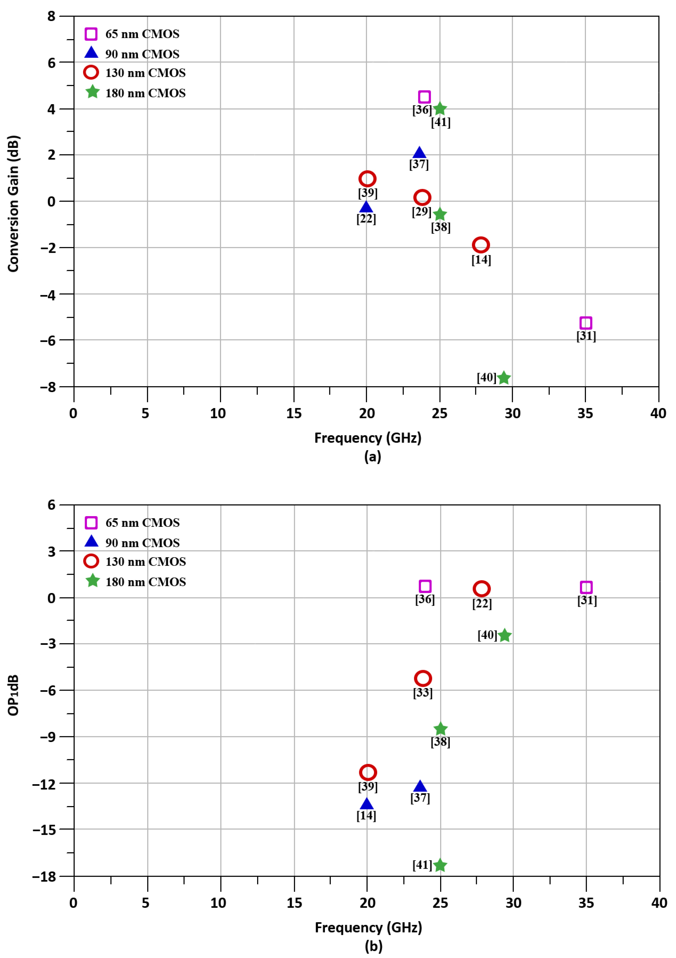
According to the author’s best knowledge, literature based on the design of CMOS up-conversion mixers operating at a particular 24 GHz frequency with high linearity and high gains is not frequently published. Figure 3 describes the literature survey of up-conversion mixers in terms of conversion gain, and OP1dB operating within the frequency range of 15–35 GHz. As our paper deals with the specific 24 GHz frequency, we made a fair comparison between the other published articles in a similar frequency range for the simplicity of the paper. Hence, the prior research shows that while the frequency range is from 15 to 35 GHz, all the authors work on the one specific parameter, i.e., to increase the conversion gain or to enhance the linearity of the up-conversion mixers. Only the previous research in [] presents a 24 GHz up-conversion mixer that achieved a high conversion gain and high linearity concurrently. This paper’s limitation is that it is confined to this idea, and it does not discuss technical details thoroughly. Furthermore, the application is limited to automotive radar applications, while our work deals with 5G applications at 24 GHz frequencies.
Figure 3.
Literature survey of up-conversion mixers [,,,,,,,,,] with operating frequencies of 15–35 GHz. (a) Conversion gain, (b) OP1dB.
In our work, the novelty lies in the fact that we are able to achieve high gain and high linearity simultaneously, with the help of our newly proposed technique. Hence, the designed up-conversion mixer includes tunable capacitive cross-coupled common source (TCC-CS) transistors to increase the gain. Furthermore, The I-DS technique also boosts the linearity. By using TCC-CS and I-DS techniques, the designed mixer archives high gain and high linearity with moderate power consumption. The up-conversion mixer achieves a peak CG of 4.1 dB at 24 GHz and the measured IP1dB of the designed mixer is 0.67 dBm at frequencies from 20 to 30 GHz, which is one of the highest-frequency up-conversion mixers among 65 nm technologies reported for 5G applications.
2. Proposed Up-Conversion Mixer Design
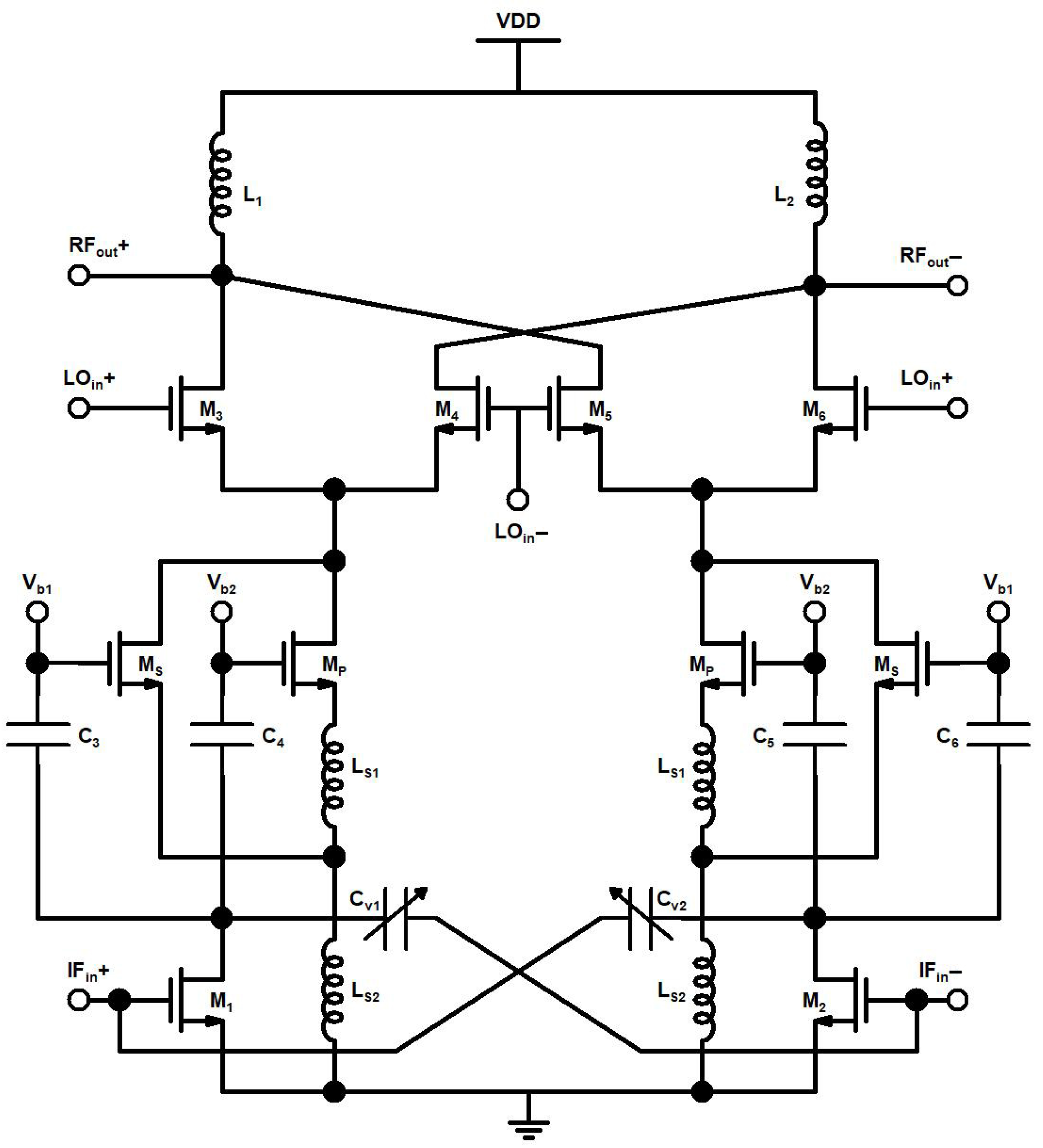
The proposed up-conversion mixer’s schematic is shown in Figure 4. The 2.4 GHz IF input signal is amplified in the Gm stage, which consists of TCC-CS and I-DS. The TCC-CS is implemented with CS transistors M1, M2, and, varactors Cv1, Cv2, the varactors are biased with tunning voltage Vt. The I-DS contains primary transistors, MP, secondary transistors, MS, dc blocking capacitors, C3–C6 and source-degenerated inductors, Ls1 and Ls2. The Ls1, and Ls2 are source-degenerated inductors of the primary and secondary transistors of I-DS. The linearized and the amplified output signal of the Gm stage is fed into the switching stage of the mixer, which comprises transistors M3–M6, and an LO signal of 21.6 GHz is applied at the gate terminal of these transistors. The Gm stage signal is translated to a 24 GHz RF output signal at the switching stage. At the RF output stage, the RF output buffer (not shown in the mixer schematic (Figure 4) for simplicity) is designed in a push/pull configuration by using a PMOS transistor (Mpb), NMOS transistor (Mnb) and feedback resistor (Rf) to match the 50 Ohm resistance.
Figure 4.
Proposed up-conversion mixer.
In the designed mixer, TCC-CS topology provides a high gain and stability, downgraded in CS topology due to parasitic gate to drain capacitances (Cgd) of transistor M1 and M2. The conventional capacitive neutralization proposed TCC-CS and the realization of a varactor in TCC-CS is shown in Figure 5a–c, respectively.
Figure 5.
(a) Conventional capacitive cross-coupling neutralization, (b) TCC-CS and (c) varactor realization in TCC-CS.
A cross-coupled capacitor Cv1 connected between the drain terminal of M1 and the gate terminal, M2m acts as a negative equivalent to capacitor Cv2, which is connected between the drain terminal of M2 and gate terminal, M1. The capacitance, Cv1 and Cv2, is used to nullify the parasitic capacitance, Cgd1, of M1 and Cgd2 of M2 as the signals across the varactor and Cgd are opposite in phase. The tunning voltage, Vt, of varactors applied at the source of transistor Mcv (Figure 5c) to cancel the effect of Cgd is small so that transistor operates in the subthreshold region and does not contribute much to the overall power consumption of mixer.
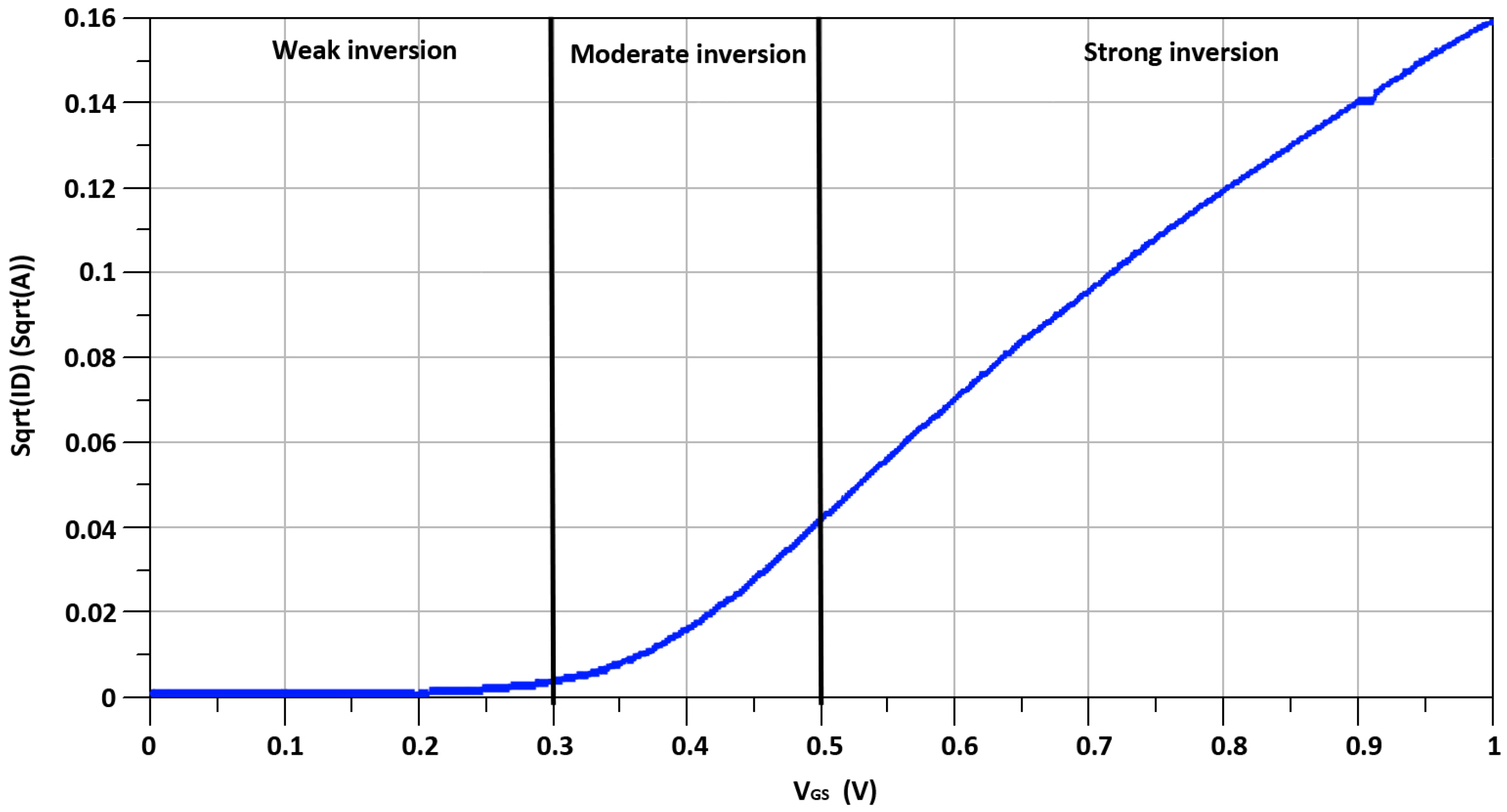
While the inclusion of I-DS in between TCC-CS topology and switching stage enhances the proposed mixer’s linearity, in I-DS, secondary transistor, Ms, is connected parallel to the primary transistor, MP. The secondary transistor of I-DS, Ms, operates in the moderate-inversion region with biasing voltage, Vb1, instead of the conventional DS technique where secondary transistors operate in the weak-inversion region. Meanwhile, primary transistors, MP, operates in the strong-inversion region with biasing voltage, Vb2. The moderate inversion region biasing of Ms helps to reduce the gate noise, which is inversely proportional to the current Ids3 of Ms. The I–V DC characteristic curve of the MOS transistors of 65 nm CMOS technology is shown in Figure 6 and Figure 7. As illustrated by the I–V DC characteristic curve, the transistor operating region can be categorized into three regions: moderate-inversion, strong-inversion and weak-inversion, depending on the transistor’s biasing conditions.
Figure 6.
I–V DC characteristic curve of the transistors with drain current Ln(ID) on the vertical-axis.
Figure 7.
I–V DC characteristic curve of the transistors with drain current sqrt(ID) on the vertical-axis.
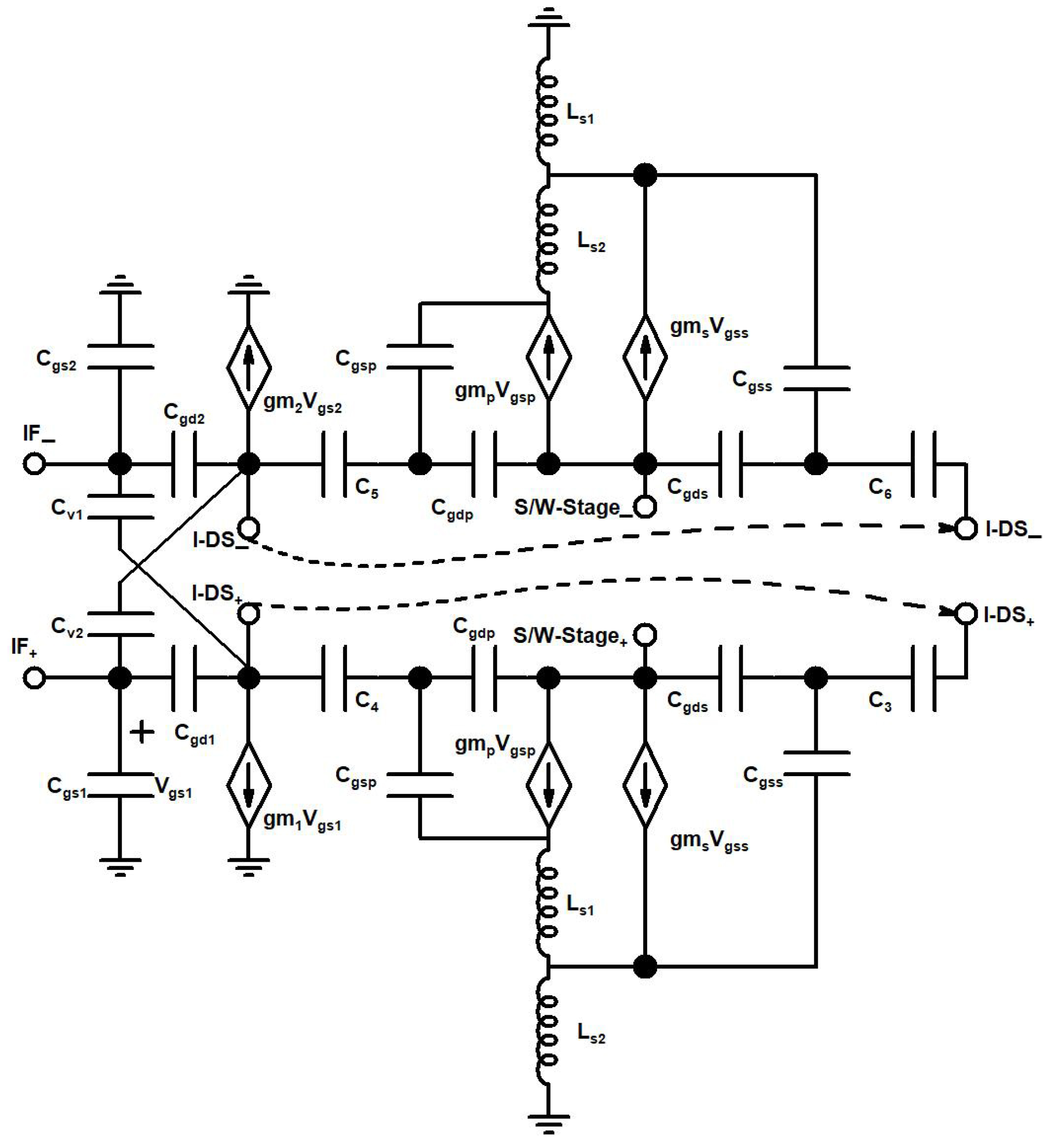
The small signal model of the transconductance stage of the designed mixer is shown in Figure 8.
Figure 8.
Small signal model of the transconductance stage.
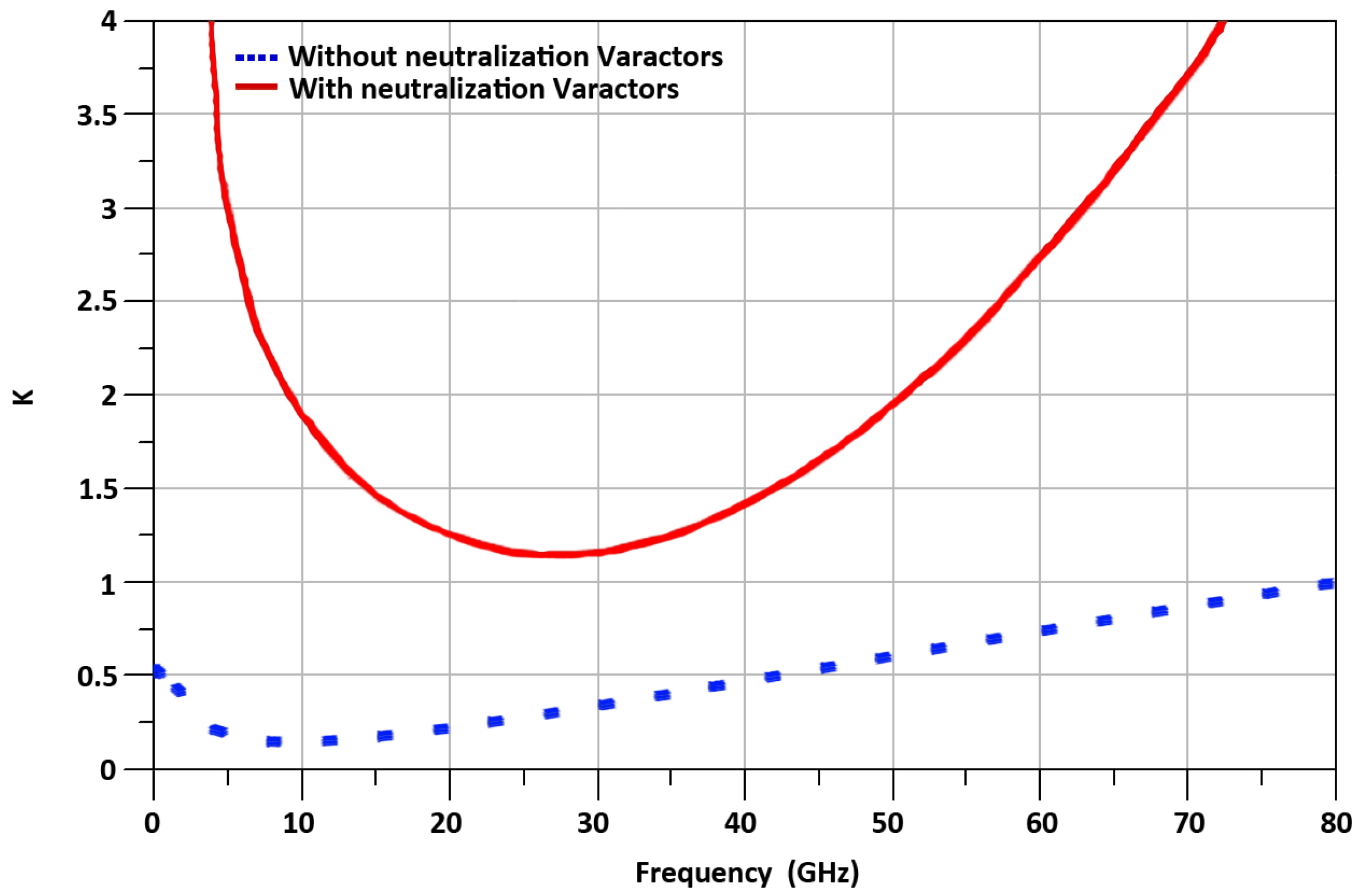
The stability factor, K, of M1 transistor of TCC-CS is shown in Equation (1) and the simulated K is shown in Figure 9. The amplifier is stable if K > 1 [].
Figure 9.
Stability Factor K.
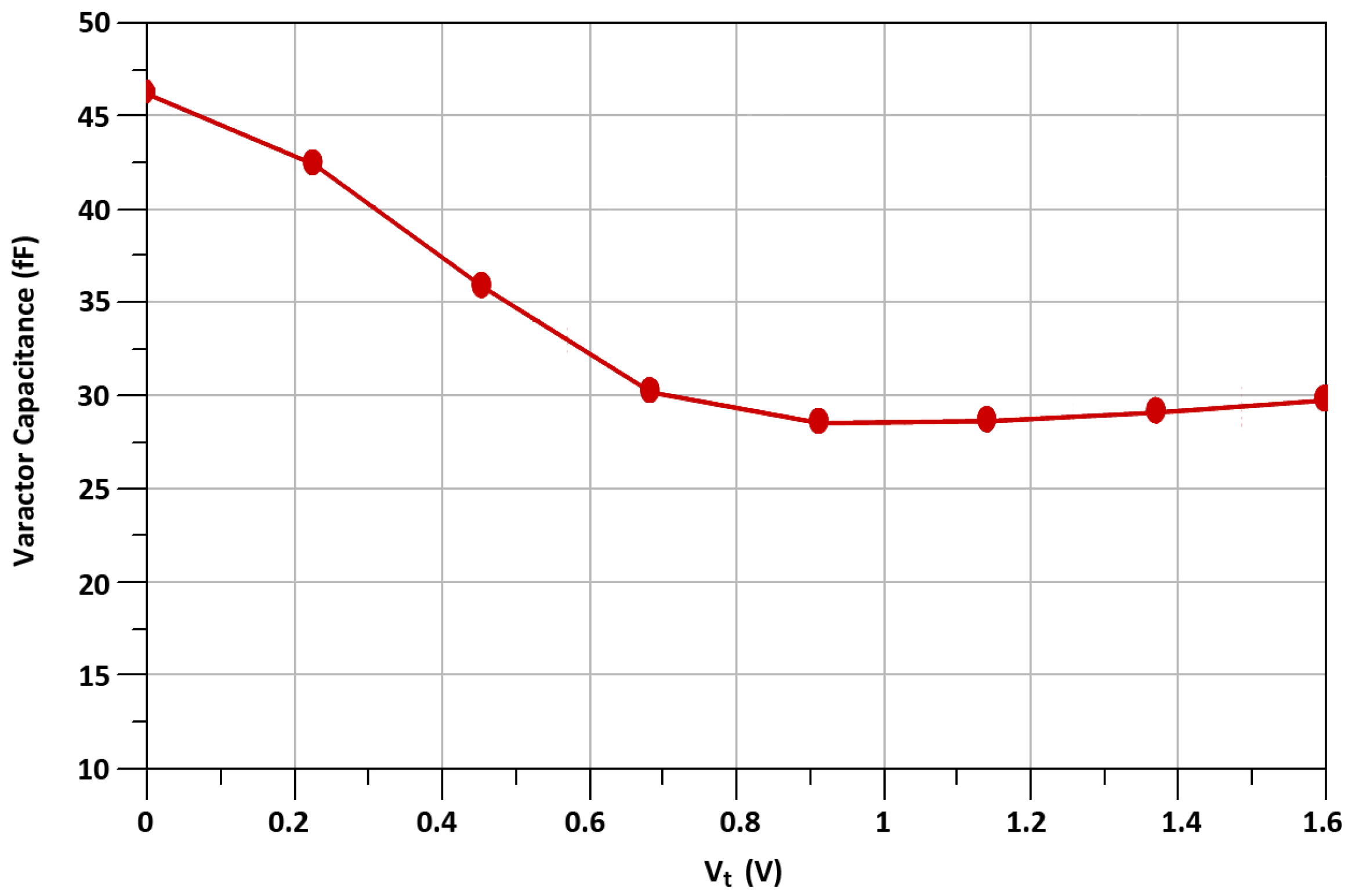
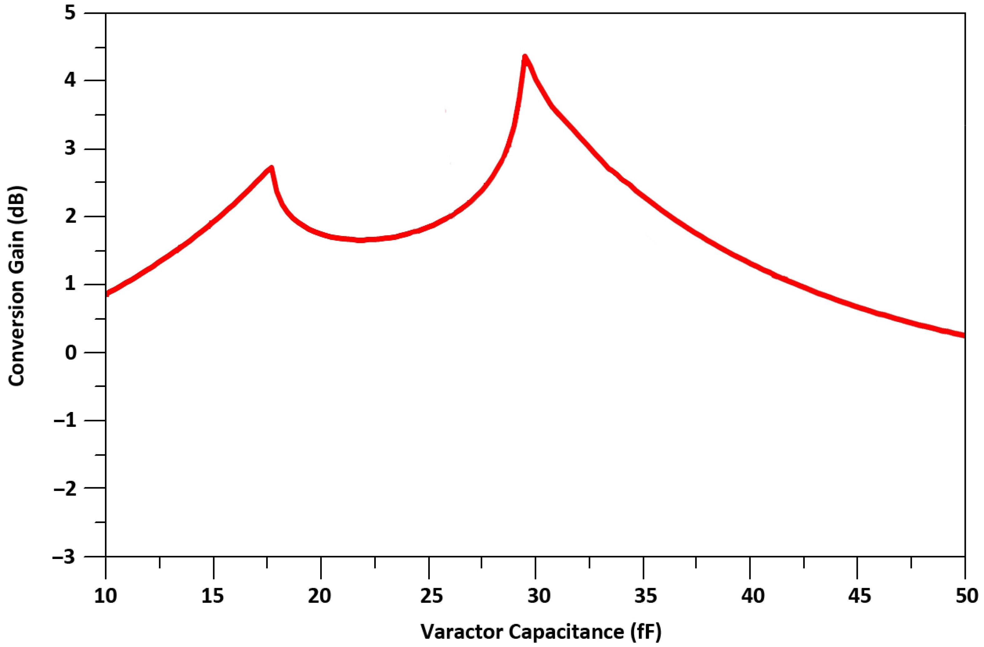
Equation (1) shows that when varactor’s capacitance Cv1 is equal to Cgd1, the stability factor is maximum. As we use a varactor’s capacitance, to neutralize the Cgd, which can be controlled externally, the PVT variations do not affect the stability of M1. The simulated varactor capacitance versus the voltage, Vt, is shown in Figure 10. The gain, G, of TCC-CS of the transconductance stage is expressed in Equation (2) and the calculated result of G versus the varator capacitance is shown in Figure 11.
Figure 10.
Varactor capacitance versus voltage Vt.
Figure 11.
Theoretical result of G.
Equation (2) shows that the TCC-CS along with stabilization also enhances the gain of the designed mixer. The device sizes of the designed mixer are shown in Table 1.
Table 1.
Designed mixer circuit component values.
2.1. Linearity Analysis
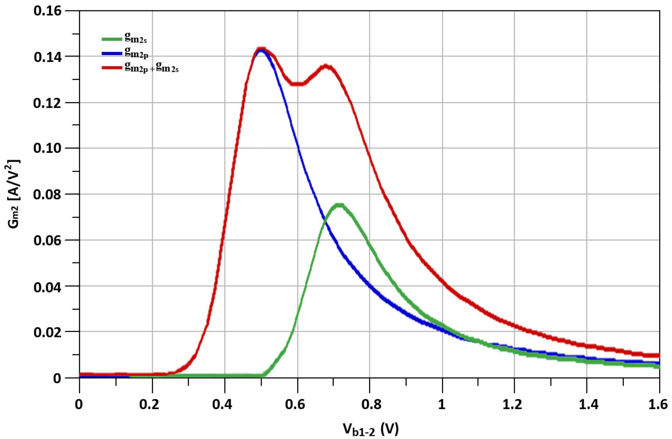
The simulated fundamental transconductances (gm), represented as, “gm1s”, “gm1p” and “gm1s + gm1p” of transistors Ms, Mp, the second-order transconductance (gm’) mentioned as “gm2s”, “gm2p” and “gm2s + gm2p” of transistosr Ms, Mp, and the third-order transconductance (gm”) noted as, “gm3s”, “gm3p” and “gm3s + gm3p” of transistors Ms, Mp with respect to biasing voltage, Vb, are shown in Figure 12, Figure 13 and Figure 14, respectively.
Figure 12.
The simulated gm1s, gm1p and gm1s + gm1p of Mp and Ms transistors.
Figure 13.
The simulated gm2s, gm2p and gm2s + gm2p of Mp and Ms transistors.
Figure 14.
The simulated gm3s, gm3p and gm3s + gm3p of Mp and Ms transistors.
When it works in the saturation region, the operating region of the CMOS transistor is classified into three different regions: weak/moderate/strong inversion regions. The primary reason for non-linearity in the CMOS transistor is the transconductance (gm) []. In the weak-inversion region, the operational speed of the CMOS transistor is slow, but the ratio of gm and drain current (Id) is high, while it is reversed in the case of the strong-inversion region of the CMOS transistor. The moderate-inversion region exhibits good operational speed and a good gm/Id ratio. The drain to source current (Ids) of a CS transistor is shown in Equation (3) [].
The gm2 and gm3 are the primary factors on which the IIP3 of the CMOS transistor depends. The IIP3 for the I-DS technique is shown in Equation (4).
where Cgss and Cgsp represent the parasitic gate-source capacitances of Ms, Mp transistors of I-DS. It is shown from Equation (4) that, by selecting proper values for Ls1 and Ls2, the effects of gm2 on the IIP3 can be reduced, which helps to improve the linearity of the designed mixer.
By carefully determining the sizes of transistors, source-degenerated inductors of the I-DS technique and with proper biasing conditions, the linearity of the proposed mixer is improved. Ls1 and Ls2 tune out the second-order non-linear components. At the same time, the third-order non-linear components can be diminished by choosing proper I-DS transistor sizes and biasing conditions [].
2.2. Layout Issues
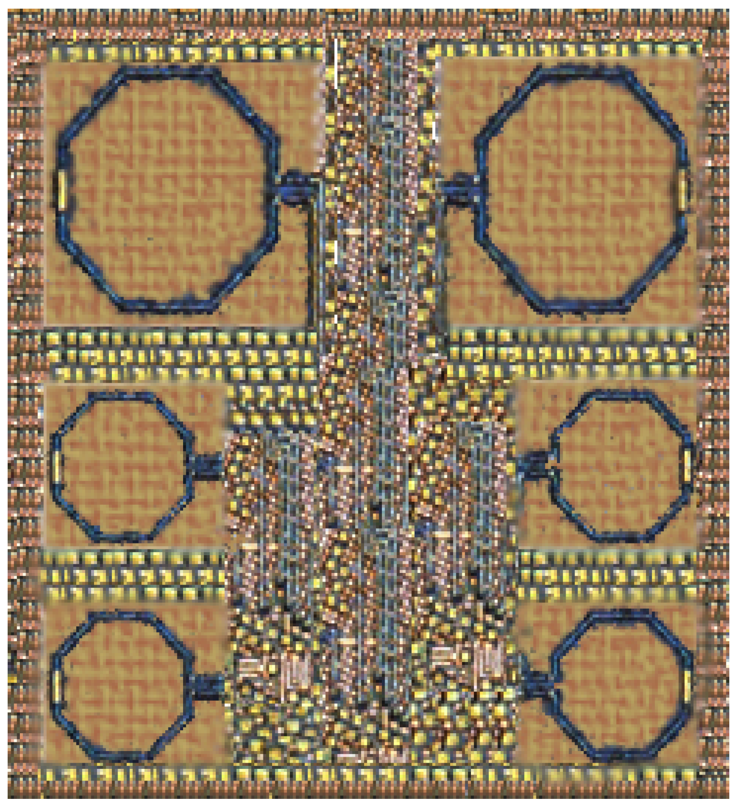
The proposed mixer, which comprises the TCC-CS, I-DS technique, is fabricated in 65 nm CMOS technology. The mixer chip microphotograph is shown in Figure 15. The mixer’s chip size is 0.4 mm (0.71 × 0.57 mm), with the exclusion of chip pads. Chip layout is carried out to ensure the stable permanence of the mixer and to reduce the parasitic resistive, capacitive and inductive effects of interconnecting lines and the parasitic capacitive effects of multiple diffusion strips. The size of transistors is divided into multiple fingers to decrease the series resistance and parasitic capacitances of the gate of transistors. Furthermore, due to multiple finger transistors, the nonlinearity due to shunt capacitance decreases and high gain is achieved. The proposed mixer’s ground layer is designed with a multi-layer technique by using different metal layers to develop a low inductive and resistive ground path. Thick and large power lines are designed to achieve the good analog current (AC) coupling between the ground and also to prevent a voltage drop. The metal insulator metal (MIM) with a capacitance of 2.2 fF/m is used to design a capacitor. Meanwhile, inductors of the mixer with a quality factor (Q) equal to 12 are designed by using metal layer 5 of 65 nm CMOS technology with 12 m thickness. To mitigate the electromagnetic interference (EMI) in between the inductors, a 16 m ground plane shield from the inductor coil is implemented.
Figure 15.
Microphotography of the up-conversion mixer.
3. Results and Discussion
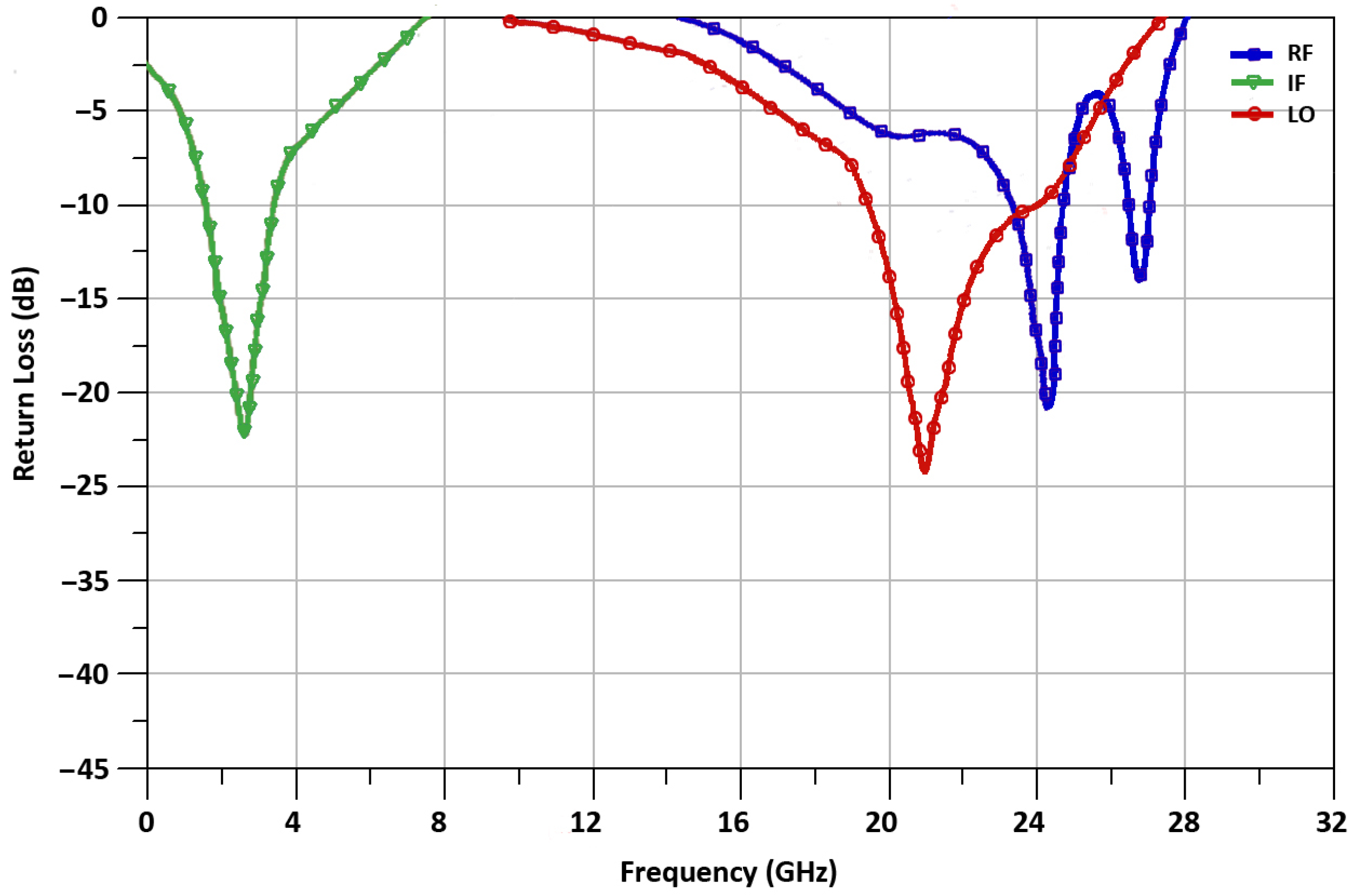
The up-conversion mixer is fabricated in 65 nm CMOS technology and the operating characteristics of the mixer are simulated and measured. The measuring probes with a ground–signal–ground–signal–ground (GSGSG) pattern are used to measure the characteristics of the mixer. The mixer operates at 1.2 V dc voltage supply, while it consumes power equal to 4.9 mW. The measured return loss of the proposed mixer is depicted in Figure 16. The IF port of the mixer at 2.4 GHz shows a return loss of −22.6 dB, the RF port of the mixer at 24 GHz shows a return loss of −20.7 dB and the LO-port of the mixer at 21.6 GHz shows a return loss of −24.8 dB.
Figure 16.
Measured return loss.
The isolation between LO-port to RF-port, RF-port to IF-port, and LO-port to IF-port of the mixer at 24 GHz is −35.1 dB, −27.3 dB, −40 dB, respectively, and it is shown in Figure 17.
Figure 17.
Isolations between mixer’s ports.
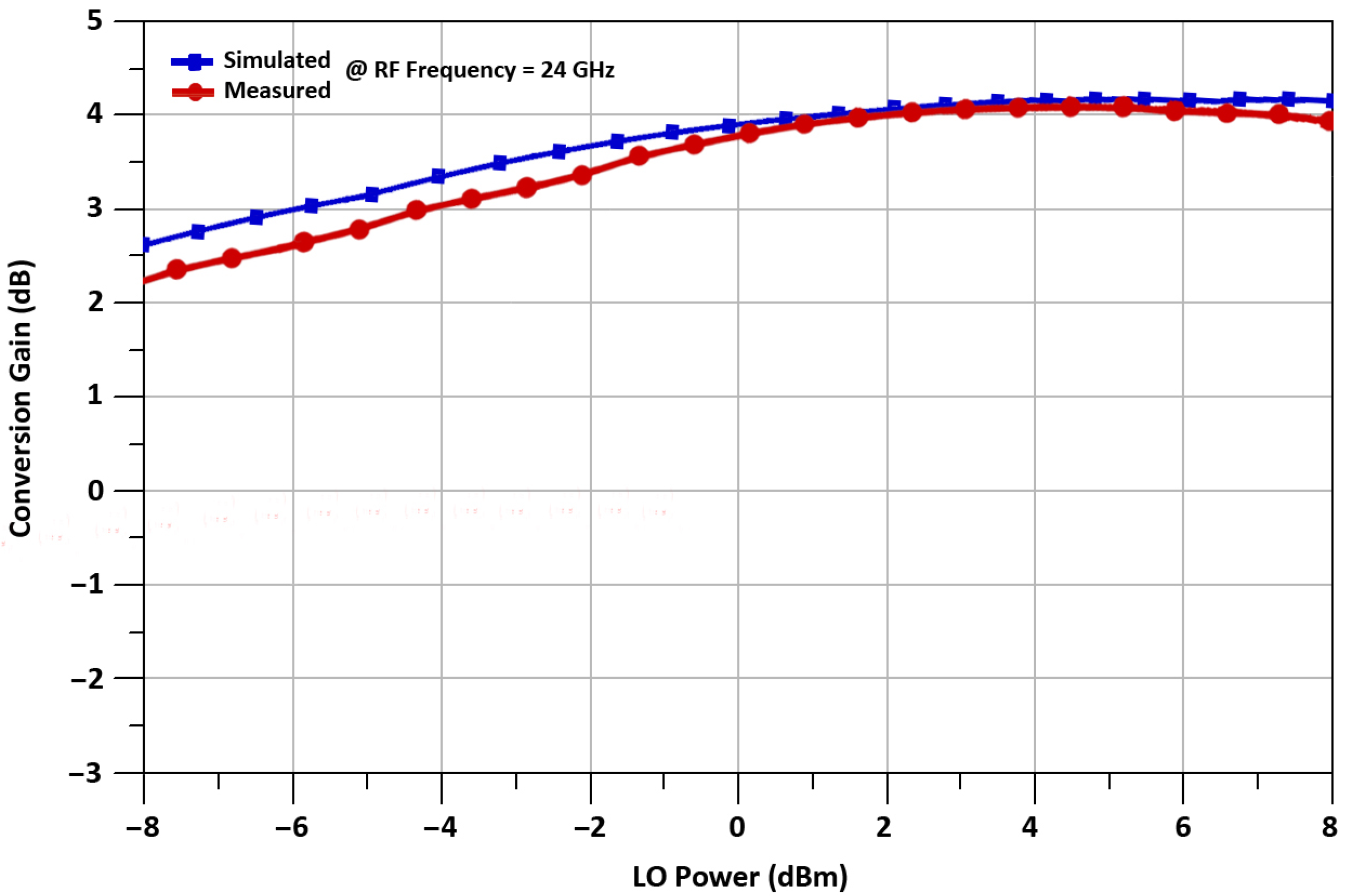
The proposed mixer’s conversion gain is simulated and measured for 24 GHz up-converted RF frequency, with the 21.6 GHz LO frequency, and 2.4 GHz IF frequency. The conversion gain increases with the increment of the LO power, but for low power operation, LO is selected to be 2 dBm. The maximum measured conversion gain at 24 GHz RF frequency is 4.1 dB. The conversion gain of a mixer is equal to 3.2 ± 0.9 dB, versus frequency from 20 to 30 GHz is illustrated in Figure 18, while conversion gain versus LO power from −8 dBm to 8 dBm is shown in Figure 19.
Figure 18.
Conversion gain vs. frequency of the mixer.
Figure 19.
Conversion gain vs. LO power of the mixer.
The linearity result of the proposed up-conversion mixer is illustrated in Figure 20, which shows input power versus output power curves. The mixer shows a measured OP1dB of 4.1 dBm, and the IP1dB is 0.67 dBm, respectively, demonstrating good linear performance.
Figure 20.
RF output power vs. IF input power.
The noise figure (NF) performance of the mixer is indicated in Figure 21. The NF of 3.8 dB at RF frequency of 24 GHz is achieved. The NF is comparatively high because of the insertion of extra transistors of I-DS transistors. The up-converted RFout+ and RFout- transient wave-forms of the designed mixer are shown in Figure 22, where up-converted RF output signal is 24 GHz. The peak–peak voltage swing of RF signal of the mixer is equal to 80 mV.
Figure 21.
Measured noise figure versus RF frequency.
Figure 22.
Output voltage waveform.
Proposed Mixer vs. State-of-the-Art Designs
The result summary of the mixer is listed in Table 2 and compared to already-published state-of-the-art designs of CMOS mixers.
Table 2.
Comparison summary for recently reported results.
4. Conclusions
A 24 GHz up-conversion mixer using 65 nm CMOS technology is proposed for 5G automobile radar applications. This paper aimed to simultaneously increase mixer gain and linearity in the 24 GHz frequency range. Therefore, we proposed a new tunable capacitive cross-coupled common source technique and linearizing I-DS technique. By using TCC-CS in the transconductance stage of the mixer, the gain and stability of the mixer were improved. Furthermore, the I-DS mitigates the third-order nonlinear coefficient and enhances linearity. The measured OP1dB of the designed mixer is 4.1 dBm, with a conversion gain of 4.1 dB at 24 GHz and 3.2 ± 0.9 dB, at frequencies from 20 to 30 GHz, and a noise figure of 3.8 dB at 24 GHz. The mixer only consumes 4.9 mW at 1.2 V. We believe that the proposed mixer has high linearity, high gain, and low DC power consumption at 24 GHz, and is best suitable for low-power 5G automobile radar applications.
Author Contributions
Conceptualization, A.S. and T.S.D.; methodology, A.S. and T.S.D.; validation, A.S. and A.H.; formal analysis, A.S.; investigation, A.S. and T.S.D.; resources, A.S. and J.-Y.R.; data curation, A.S. and M.R.B.; writing—original draft preparation, A.S., T.S.D. and P.B.; writing—review and editing, A.S., A.H. and J.-Y.R.; supervision, A.S., A.H. and J.-Y.R.; funding acquisition, J.-Y.R. All authors have read and agreed to the published version of the manuscript.
Funding
We are thankful to the Sejong University research department for supervising and sponsoring this research publication.
Institutional Review Board Statement
Not applicable.
Informed Consent Statement
Not applicable.
Data Availability Statement
Not applicable.
Acknowledgments
This research was supported by the Basic Science Research Program through the *National Research Foundation of Korea* (NRF) funded by the Ministry of Education (2018R1D1A1B07043286).
Conflicts of Interest
The authors declare no conflict of interest.
References
- Qayyum, J.A.; Albrecht, J.D.; Ulusoy, A.C. A compact V-band upconversion mixer with −1.4 dBm OP1dB in SiGe HBT technology. IEEE Microw. Wirel. Components Lett. 2019, 29, 276–278. [Google Scholar] [CrossRef]
- Ayesha, A.; Rahman, M.; Haider, A.; Majeed Chaudhry, S. On Self-Interference Cancellation and Non-Idealities Suppression in Full-Duplex Radio Transceivers. Mathematics 2021, 9, 1434. [Google Scholar] [CrossRef]
- Siddique, A.; Delwar, T.S.; Kurbanov, M.; Ryu, J.Y. Low-power low-phase noise VCO for 24 GHz applications. Microelectron. J. 2020, 97, 104720. [Google Scholar] [CrossRef]
- Chen, Q.B.; Schaeffer, J.K. 22FDX Embracing IoT, 5G, and Automotive Applications-A Perspective through Global Research. In Proceedings of the 2019 IEEE SOI-3D-Subthreshold Microelectronics Technology Unified Conference (S3S), San Jose, CA, USA, 14–17 October 2019; pp. 1–5. [Google Scholar]
- Siddique, A.; Ryu, J.Y. A 24 GHz frequency synthesizer for automotive collision avoidance radar. Int. J. Electron. Lett. 2020, 8, 1–16. [Google Scholar] [CrossRef]
- Li, D.; Xia, Q.; Huang, J.; Li, J.; Chang, H.; Sun, B.; Liu, H. A 24 GHz Direct Conversion Receiver for FMCW Ranging Radar Based on Low Flicker Noise Mixer. Electronics 2021, 10, 722. [Google Scholar] [CrossRef]
- Voltti, M.; Koivisto, T.; Tiiliharju, E. Comparison of active and passive mixers. In Proceedings of the 2007 18th European Conference on Circuit Theory and Design, Seville, Spain, 27–30 August 2007; pp. 890–893. [Google Scholar]
- El-Desouki, M.M.; Qasim, S.M.; BenSaleh, M.S.; Deen, M.J. Toward realization of 2.4 GHz balunless narrowband receiver front-end for short range wireless applications. Sensors 2015, 15, 10791–10805. [Google Scholar] [CrossRef] [PubMed] [Green Version]
- Zumbahlen, H. Linear Circuit Design Handbook; Newnes/Elsevier: Wilmington, MA, USA, 2008. [Google Scholar]
- Siddiqi, A.A. Design Methodology and Investigation of GHz Range CMOS RF Mixers. Master’s Thesis, Carleton University, Ottawa, ON, Canada, 2000. [Google Scholar]
- Asad, B.Z.J. Low-Noise 24 GHz 0.15 μm GaAs pHEMT Gilbert Cell Mixer for Intelligent Transportation System Radar Receiver. Master’s Thesis, Ottawa-Carleton Institute for Electrical and Computer Engineering, Ottawa, ON, Canada, 2014. [Google Scholar]
- Arun, J.; Ezra, K.; Nithin, M.; Ravi, S. Design and Analysis of Double Balanced Gilbert Cell CMOS Mixer for Heterodyne receivers. Int. J. Appl. Eng. Res. 2013, 8, 2413–2416. [Google Scholar]
- Hu, X. RF CMOS Tunable Gilbert Mixer with Wide Tuning Frequency and Controllable Bandwidth: Design Sythesis and Verification. Master’s Thesis, Department of Electrical Engineering, Wright State University, Dayton, OH, USA, 2017. [Google Scholar]
- Ellinger, F.; Rodoni, L.C.; Sialm, G.; Kromer, C.; von Buren, G.; Schmatz, M.L.; Menolfi, C.; Toifl, T.; Morf, T.; Kossel, M.; et al. 30–40-GHz drain-pumped passive-mixer MMIC fabricated on VLSI SOI CMOS technology. IEEE Trans. Microw. Theory Technol. 2004, 52, 1382–1391. [Google Scholar] [CrossRef]
- Yang, H.-Y.; Tsai, J.-H.; Huang, T.-W.; Wang, H. Analysis of a new 33–58-GHz doubly balanced drain mixer in 90-nm CMOS technology. IEEE Trans. Microw. Theory Technol. 2012, 60, 1057–1068. [Google Scholar] [CrossRef]
- Sedighi, S.; Hashemipour, O.; Dousti, M. A 2.4-GHz highly linear derivative superposition Gilbert cell mixer. Turk. J. Electr. Eng. Comput. Sci. 2016, 24, 571–579. [Google Scholar] [CrossRef]
- Murad, S.A.Z.; Shahimin, M.M.; Pokharel, R.K.; Kanaya, H.; Yoshida, K. Linearity improvement of 5.2-GHz CMOS up-conversion mixer for wireless applications. Microw. Opt. Technol. Lett. 2012, 54, 923–925. [Google Scholar] [CrossRef]
- Zhang, F.; Skafidas, E.; Shieh, W.; Yang, B.; Wicks, B.N.; Liu, Z. A 60-GHz double-balanced mixer for direct up-conversion transmitter on 130-nm CMOS. In Proceedings of the 2008 IEEE Compound Semiconductor Integrated Circuits Symposium, Monterey, CA, USA, 12–15 October 2008; pp. 1–4. [Google Scholar]
- Won, Y.S.; Kim, C.H.; Lee, S.G. A 24 GHz Highly Linear Up-Conversion Mixer in CMOS 0.13 μm Technology. IEEE Microw. Wirel. Components Lett. 2015, 25, 400–402. [Google Scholar] [CrossRef]
- Wan, Q.; Wang, C.; Sun, J. Design of a low voltage highly linear 2.4 GHz up-conversion mixer in 0.18 μm CMOS technology. Wirel. Pers. Commun. 2013, 70, 57–68. [Google Scholar] [CrossRef]
- Siddique, A.; Delwar, T.S.; Ryu, J.Y. A high-linearity high-gain up-conversion mixer for 24 GHz automotive radar applications. Electron. Lett. 2021, 57, 48–50. [Google Scholar] [CrossRef]
- Xavier, B.A.; Sullivan, P.J.; Fransis, B.; Ku, W. A 0.9 V 960 MHz CMOS radio front end employing a doubly balanced transconductance mixer. In Proceedings of the Solid-State Circuits Conference, Southampton, UK, 16–18 September 1997; pp. 404–407. [Google Scholar]
- Lin, Y.S.; Wen, W.C.; Wang, C.C. 13.6 mW 79 GHz CMOS up-conversion mixer with 2.1 dB gain and 35.9 dB LO-RF isolation. IEEE Microw. Wirel. Components Lett. 2013, 24, 126–128. [Google Scholar] [CrossRef]
- Chen, A.Y.K.; Baeyens, Y.; Chen, Y.K.; Lin, J. An 80 GHz High Gain Double-Balanced Active Up-Conversion Mixer Using 0.18 μm SiGe BiCMOS Technology. IEEE Microw. Wirel. Components Lett. 2011, 21, 326–328. [Google Scholar] [CrossRef]
- Lee, C.P.; Behzad, A.; Ojo, D.; Kappes, M.; Au, S.; Pan, M.A.; Carter, K.; Tian, S. A highly linear direct-conversion transmit mixer transconductance stage with local oscillation feedthrough and I/Q imbalance cancellation scheme. In Proceedings of the 2006 IEEE International Solid State Circuits Conference—Digest of Technical Papers, San Francisco, CA, USA, 6–9 February 2006; pp. 1450–1459. [Google Scholar]
- Syu, J.-S.; Meng, C. 2.4/5.7 GHz dual-band high linearity Gilbert upconverter utilizing bias-offset TCA and LC current combiner. IEEE Microw. Compon. Lett. 2007, 17, 876–878. [Google Scholar] [CrossRef]
- Chiou, H.-K.; Chou, H.-T. A 0.4 V microwatt power consumption current-reused up-conversion mixer. IEEE Microw. Compon. Lett. 2013, 23, 40–42. [Google Scholar] [CrossRef]
- Codega, N.; Rossi, P.; Pirola, A.; Liscidini, A.; Castello, R. A currentmode, low out-of-band noise LTE transmitter with a class-A/B power mixer. IEEE J. Solid-State Circuits 2014, 49, 1627–1638. [Google Scholar] [CrossRef]
- Li, J.; Gu, Q.J. Harmonic-based nonlinearity factorization of switching behavior in up-conversion mixers. IEEE Trans. Circuits Syst. Reg. Pap. 2019, 66, 2468–2477. [Google Scholar] [CrossRef]
- Wang, X.; Dengi, A.; Kiaei, S. A high IIP3 -band BiCMOS mixer for radar applications. Proc. Int. Circuits Syst. Symp. 2004, 1, I-113–I-116. [Google Scholar]
- Gilbert, B. The micromixer: A highly linear variant of the Gilbert mixer using a bisymmetric class-AB input stage. IEEE Solid-State Circuits 1997, 32, 1412–1423. [Google Scholar] [CrossRef]
- Tseng, S.C.; Meng, C.C.; Chang, C.-H.; Wu, C.-K.; Huang, G.-W. Monolithic broadband Gilbert micromixer with an integrated Marchand balun using standard silicon ic process. IEEE Trans. Microw. Theory Technol. 2006, 54, 4362–4371. [Google Scholar] [CrossRef] [Green Version]
- Sivonen, P.; Vilander, A.; Parssinen, A. Cancellation of second orderintermodulation distortion and enhancement of IIP2 in common source and common-emitter RF transconductors. IEEE Trans. Circuits Syst. Reg. Pap. 2005, 52, 305–317. [Google Scholar] [CrossRef]
- Bao, M.; Li, Y.; Cathelin, A. A 23 GHz active mixer with integrated diode linearizer in SiGe BiCMOS technology. In Proceedings of the 33rd European Microwave Conference Proceedings (IEEE Cat. No.03EX723C), Munich, Germany, 7 October 2003; pp. 391–393. [Google Scholar]
- Tseng, S.-C.; Meng, C.C.; Wu, C.-K. GaInP/GaAs HBT wideband transformer Gilbert downconverter with low voltage supply. Electron. Lett. 2008, 44, 127–128. [Google Scholar] [CrossRef] [Green Version]
- Chen, J.H.; Kuo, C.C.; Hsin, Y.M.; Wang, H. A 15–50 GHz broadband resistive FET ring mixer using 0.18 μm CMOS technology. In Proceedings of the 2010 IEEE MTT-S International Microwave Symposium, Anaheim, CA, USA, 23–28 May 2010; pp. 784–787. [Google Scholar]
- Lai, I.C.; Fujishima, M. An integrated 20–26 GHz CMOS up-conversion mixer with low power consumption. In Proceedings of the 32nd European Solid-State Circuits Conference, Montreaux, Switzerland, 19–21 September 2006; pp. 400–403. [Google Scholar]
- Comeau, J.P.; Cressler, J.D. A 28-GHz SiGe up-conversion mixer using a series-connected triplet for higher dynamic range and improved IF port return loss. IEEE J. Solid-State Circuits 2006, 41, 560–565. [Google Scholar] [CrossRef]
- Lin, Y.H.; Li, Y.C.; Lin, W.J.; Tsai, J.H.; Alshehri, A.; Almalki, M.; Sayed, A.; Huang, T.W. A Ka-band High Linearity Up-Conversion Mixer with LO Boosting Linearization Technique. In Proceedings of the 2018 48th European Microwave Conference (EuMC), Madrid, Spain, 23–27 September 2018; pp. 259–262. [Google Scholar]
- Madihian, M.; Desclos, L.; Maruhashi, K.; Onda, K.; Kuzuhara, M. A monolithic AlGaAs/InGaAs upconverter IC for K-Band wireless networks. IEEE Trans. Microw. Theory Tech. 1995, 43, 2773–2777. [Google Scholar] [CrossRef]
- Tsai, J.-H.; Lin, W.-H.; Huang, C.-J. Design of 15–34 GHz low-power up-conversion ring mixer using 0.18 μm CMOS technology. In Proceedings of the 2016 IEEE International Symposium on Radio-Frequency Integration Technology (RFIT), Taipei, Taiwan, 24–26 August 2016; pp. 1–3. [Google Scholar]
- Aparin, V.; Larson, L.E. Modified derivative superposition method for linearizing FET low-noise amplifiers. IEEE Trans. Microw. Theory Tech. 2005, 53, 571–581. [Google Scholar] [CrossRef]
- Chen, Z.; Liu, Z.; Jiang, Z.; Liu, P.; Liu, H.; Wu, Y.; Zhao, C.; Kang, K. A 27.5–43.5 GHz high linearity up-conversion CMOS mixer for 5G communication. In Proceedings of the 2017 IEEE Electrical Design of Advanced Packaging and Systems Symposium (EDAPS), Haining, China, 14–16 December 2017; pp. 1–3. [Google Scholar]
- Valdes-Garcia, A.; Reynolds, S.; Plouchart, J.-O. 60 GHz transmitter circuits in 65 nm CMOS. In Proceedings of the 2008 IEEE Radio Frequency Integrated Circuits Symposium, Atlanta, GA, USA, 15–17 June 2008; pp. 641–644. [Google Scholar]
- Verma, A.; O, K.K.; Lin, J. A low-power up conversion CMOS mixer for 22–29-GHz ultra-wideband applications. IEEE Trans. Microw. Theory Tech. 2006, 54, 3295–3300. [Google Scholar] [CrossRef]
- Zhu, F.; Wang, K.; Wu, K. A reconfigurable low-voltage and low-power millimeter-wave dual-band mixer in 65-nm CMOS. IEEE Access 2019, 7, 33359–33368. [Google Scholar] [CrossRef]
- Motieifar, A.; Pour, Z.A.; Bridges, G.; Shafai, C.; Shafai, L. An ultra wideband mixer with integrated impedance-matching circuit. In Proceedings of the 2006 12th International Symposium on Antenna Technology and Applied Electromagnetics and Canadian Radio Sciences Conference, Montreal, QC, Canada, 17–19 July 2006; pp. 1–4. [Google Scholar]
- Wan, Q.; Wang, C.; Yu, F. Design of a 2.4 GHz High-Performance Up-Conversion Mixer with Current Mirror Topology. Radioengineering 2012, 21, 752–757. [Google Scholar]
- Sapone, G.; Palmisano, G. A 1.5-V 0.25-μm CMOS up-converter for 3–5 GHz low-power WPANs. Microw. Opt. Technol. Lett. 2007, 49, 2209–2212. [Google Scholar] [CrossRef]
Publisher’s Note: MDPI stays neutral with regard to jurisdictional claims in published maps and institutional affiliations. |
© 2021 by the authors. Licensee MDPI, Basel, Switzerland. This article is an open access article distributed under the terms and conditions of the Creative Commons Attribution (CC BY) license (https://creativecommons.org/licenses/by/4.0/).