
Design of SiC-Doped Piezoresistive Pressure Sensor for High-Temperature Applications


 , and
, and
Abstract
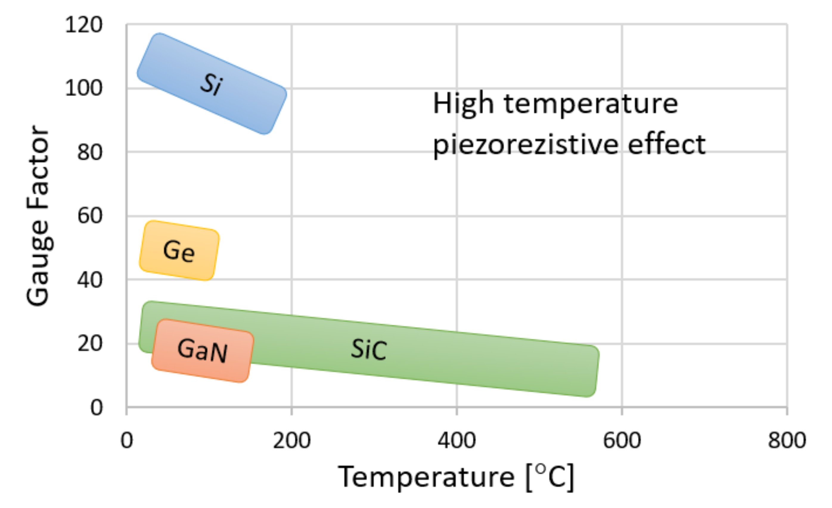
:1. Introduction
2. Materials and Methods
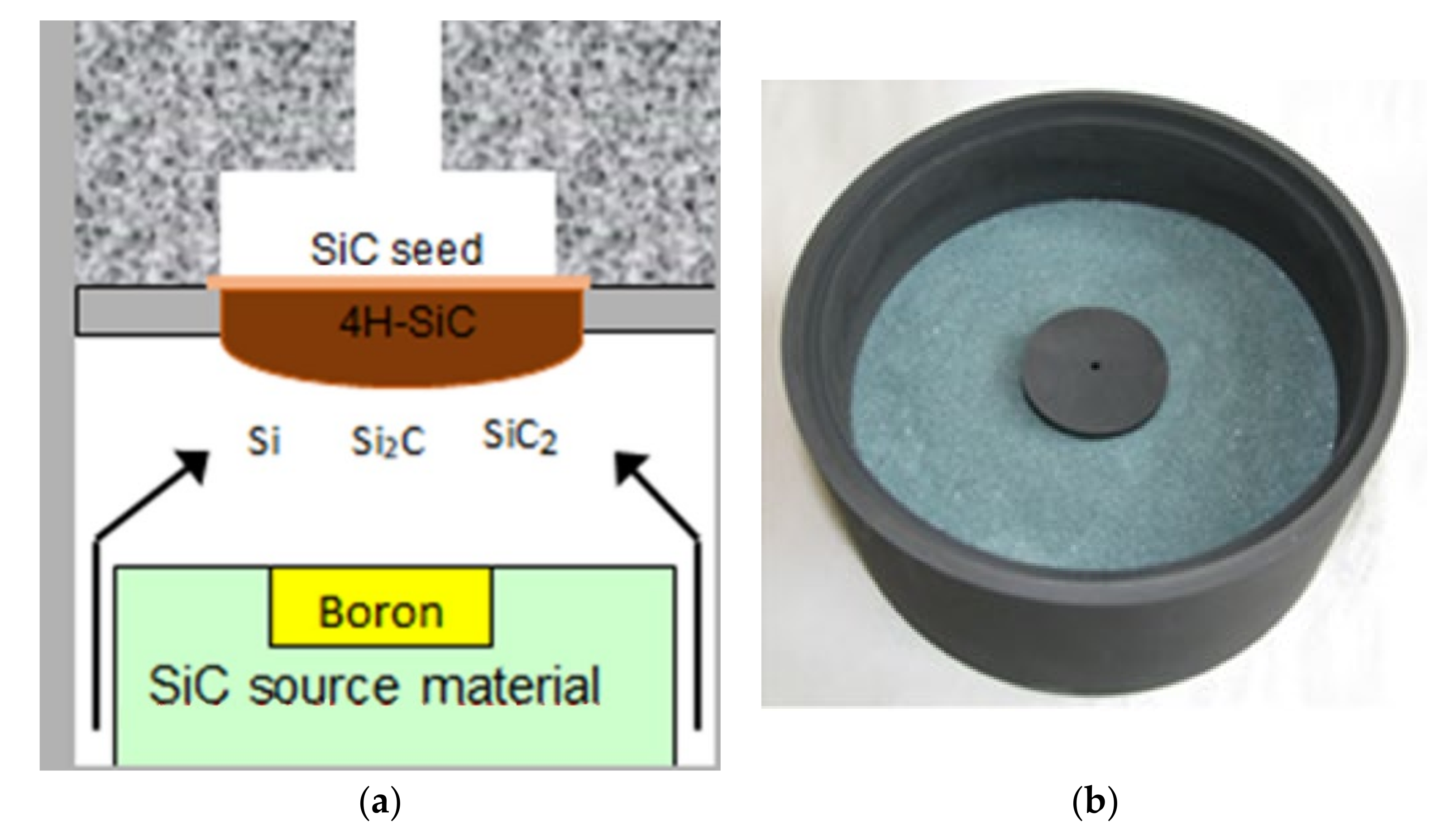
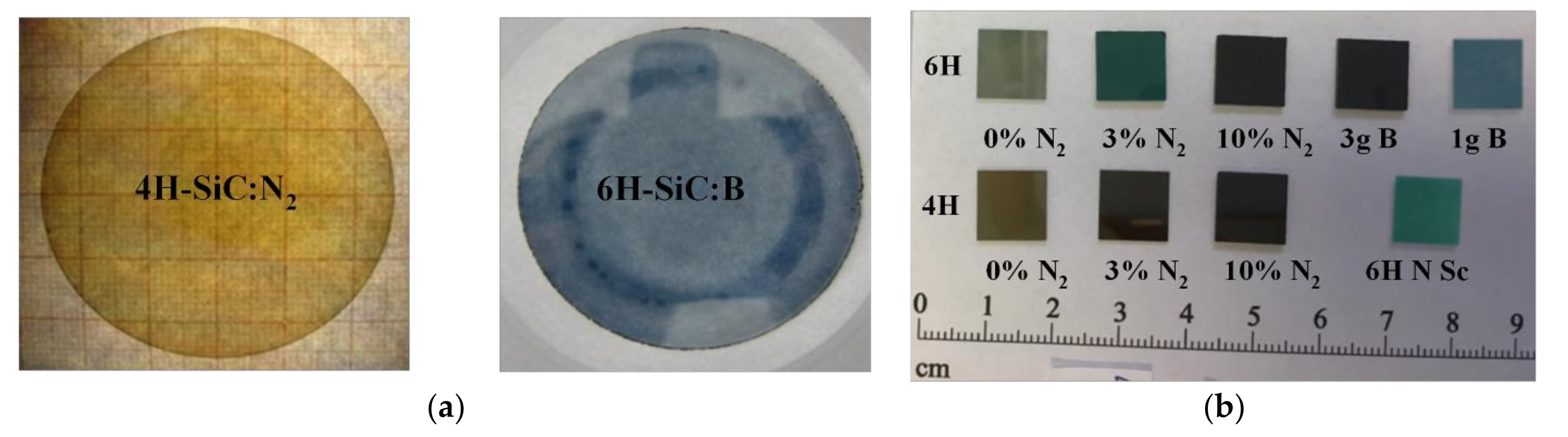
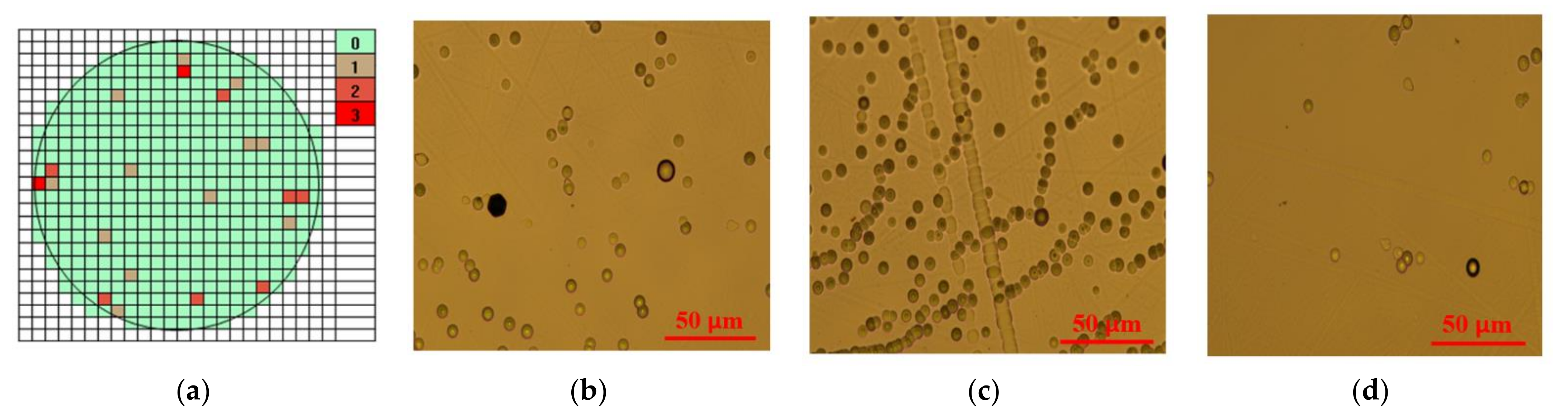
2.1. Bulk Crystals Manufacturing and Characterization
2.2. Layered Materias Fabrication and Characterization
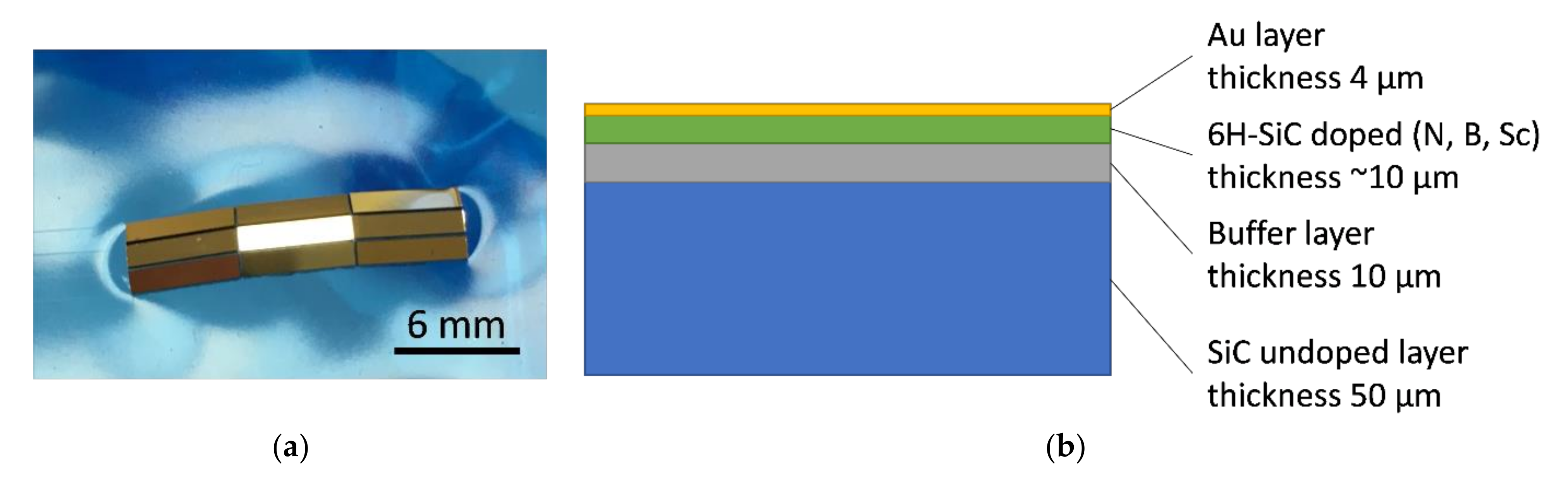
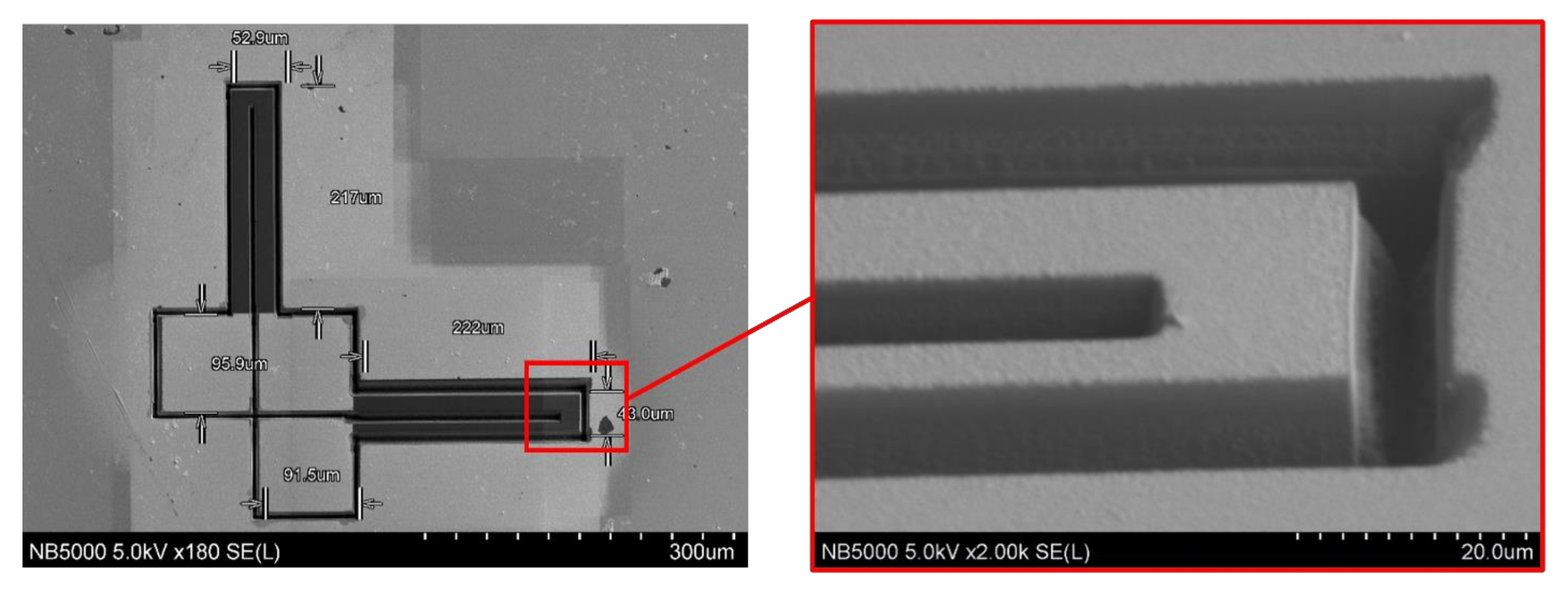
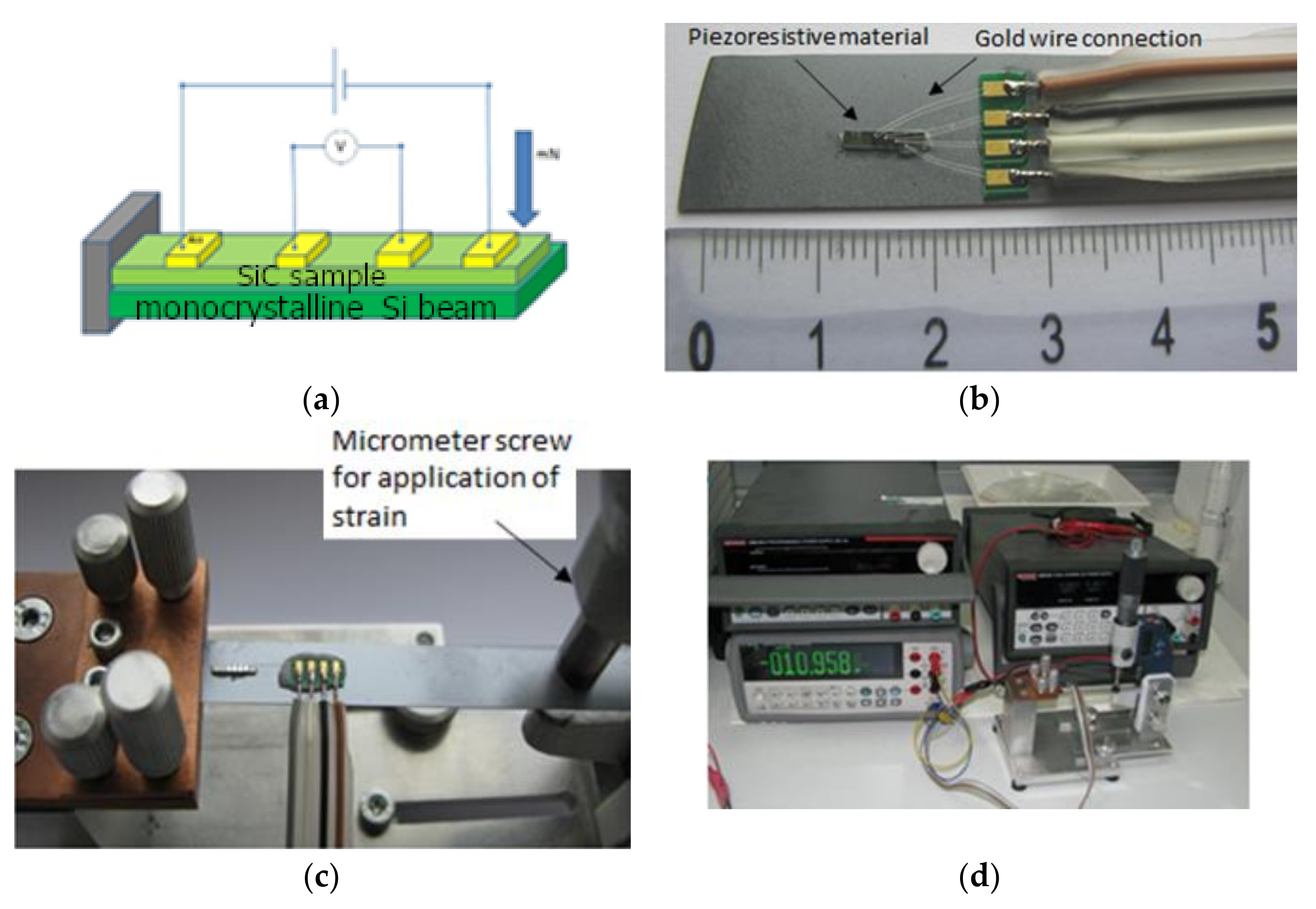
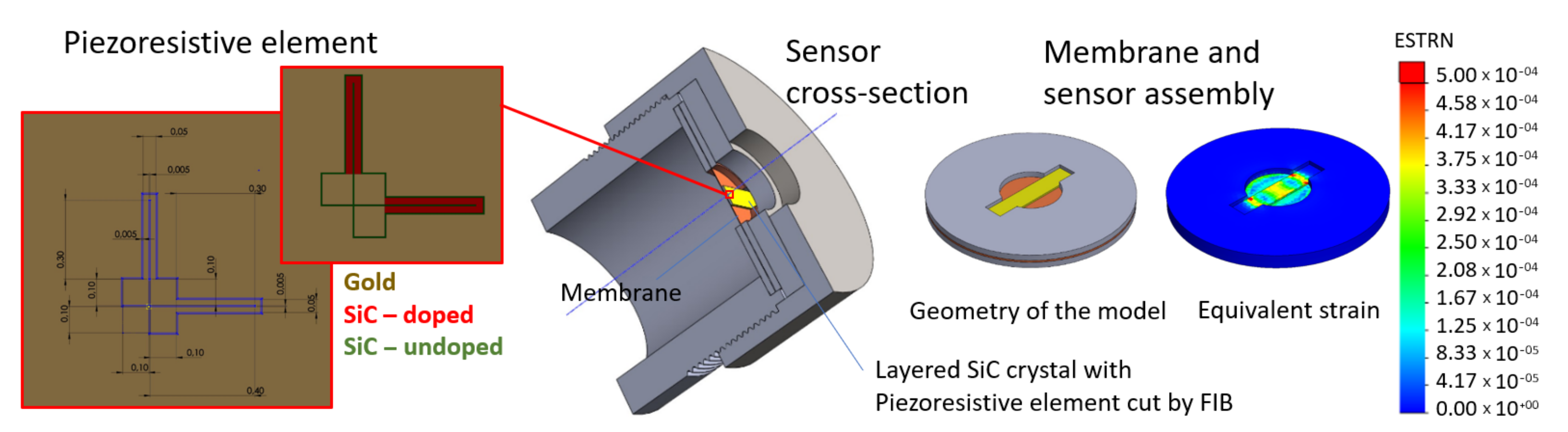
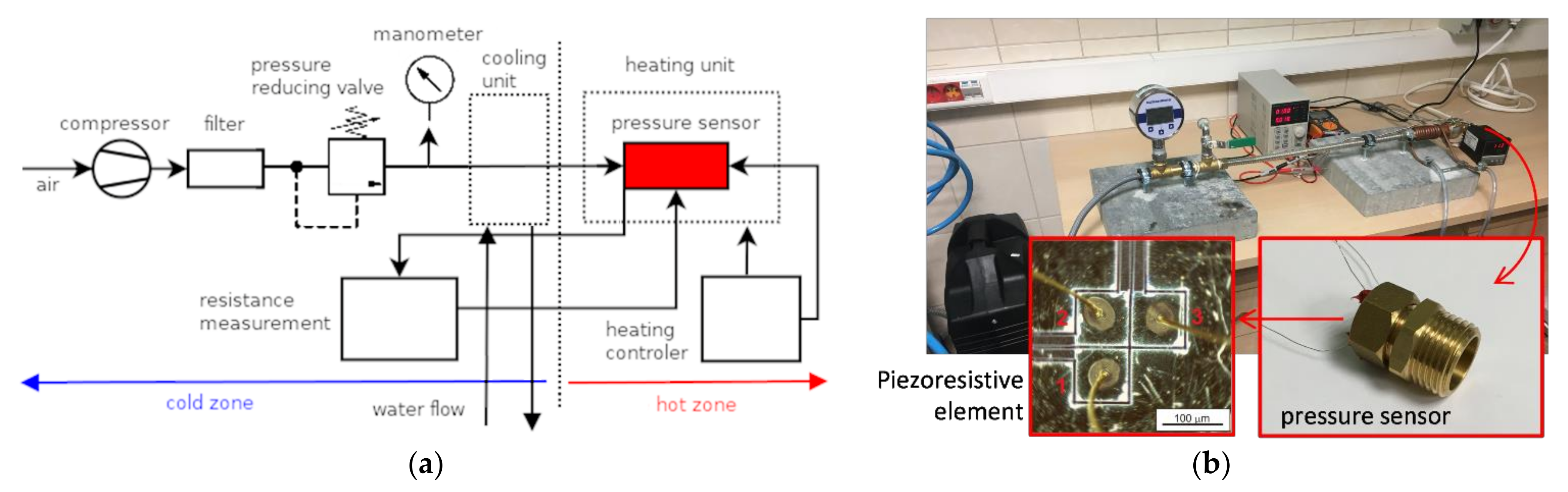
2.3. Design, Fabrication, and Characterization of Pressure Sensors
3. Results and Discussion
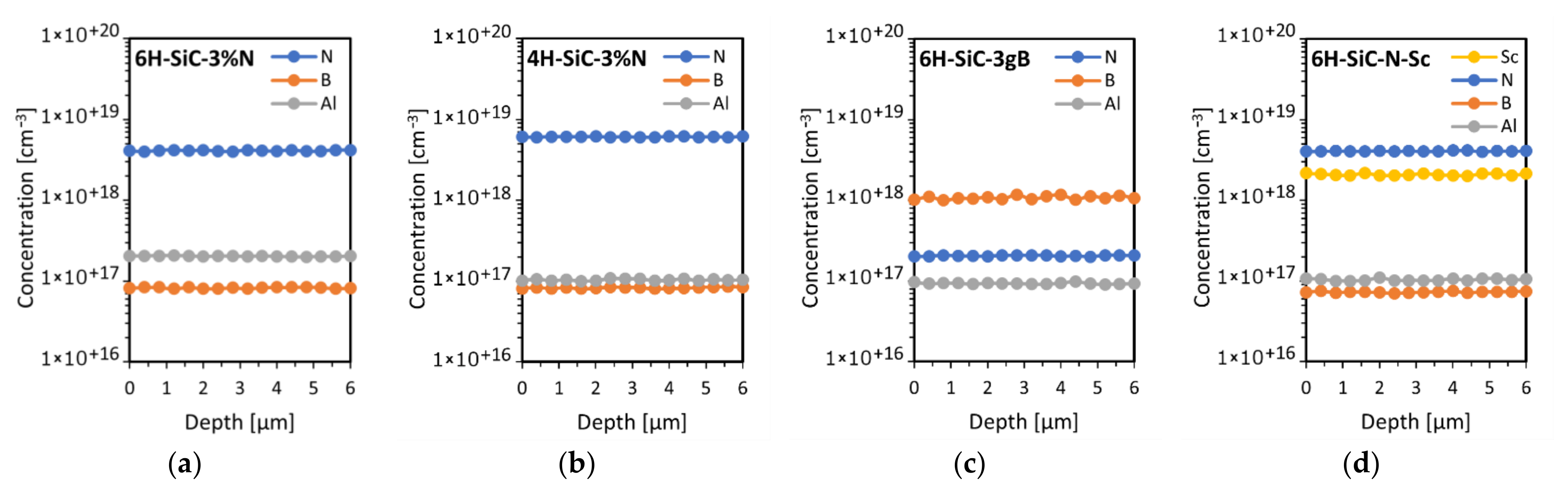
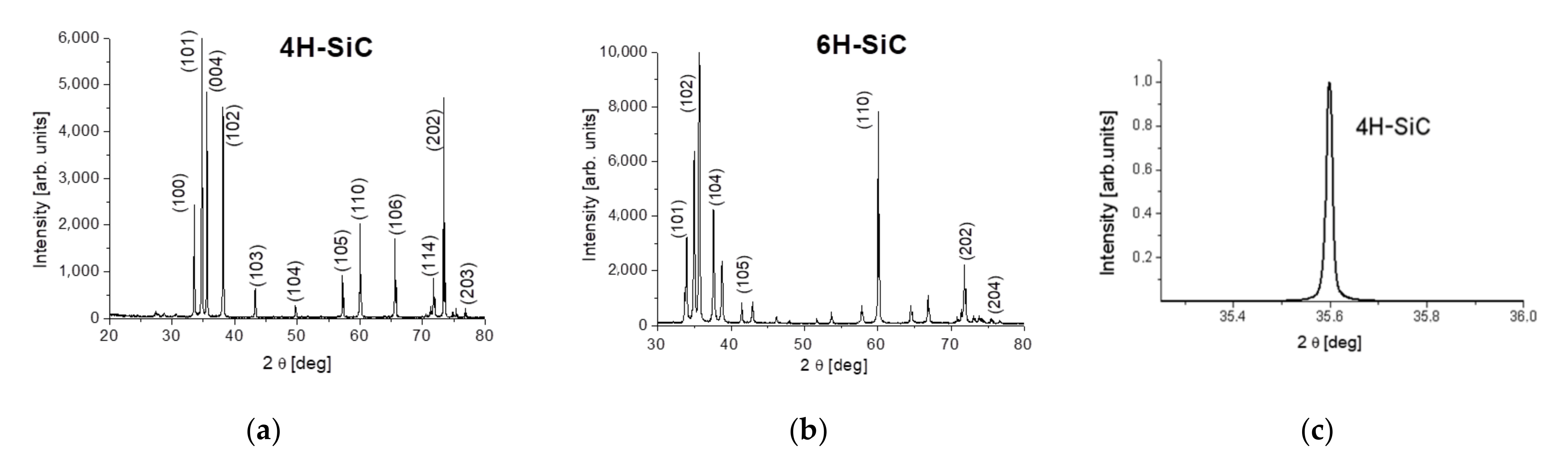
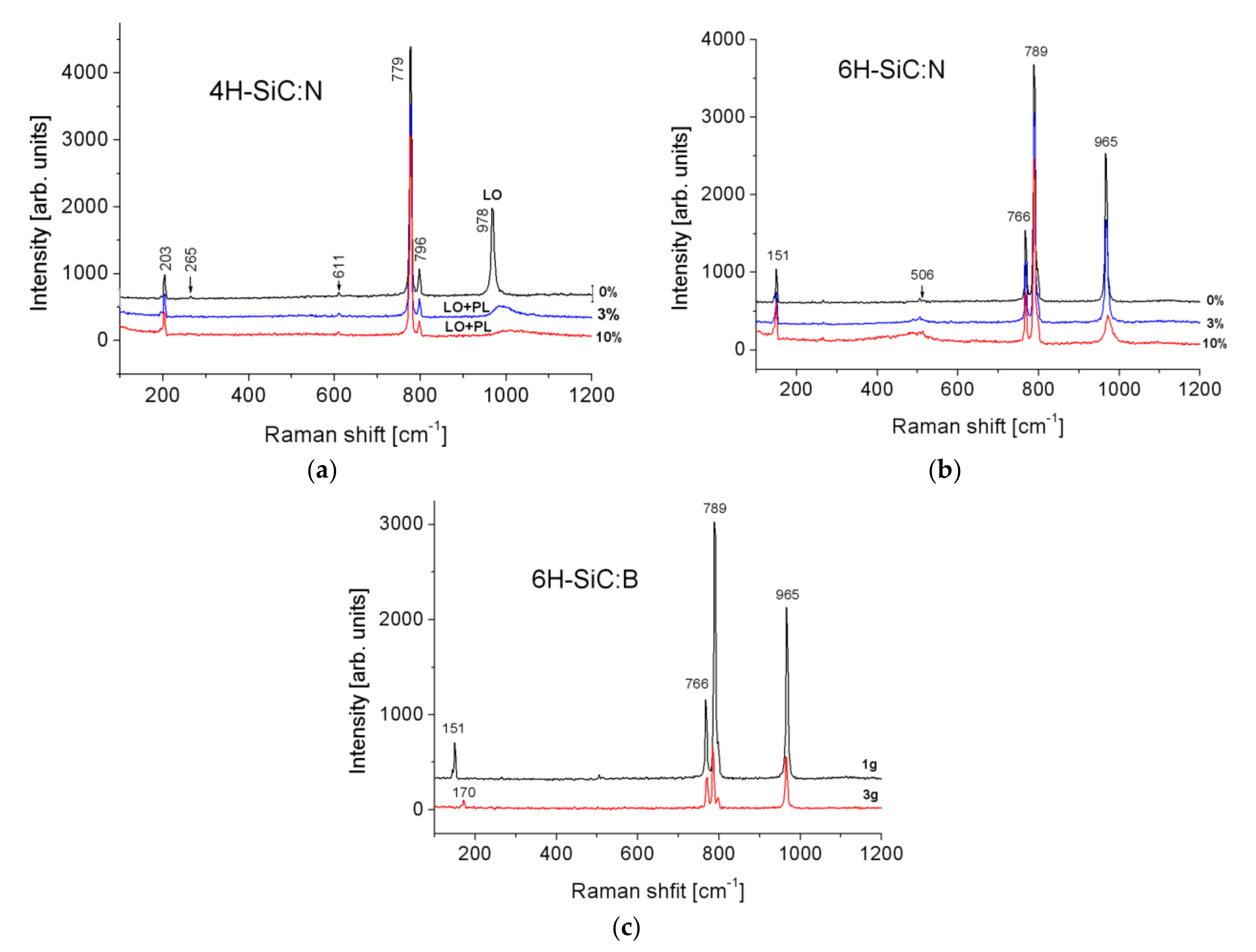
3.1. STRUCTURE and Properties of Doped Bulk SiC
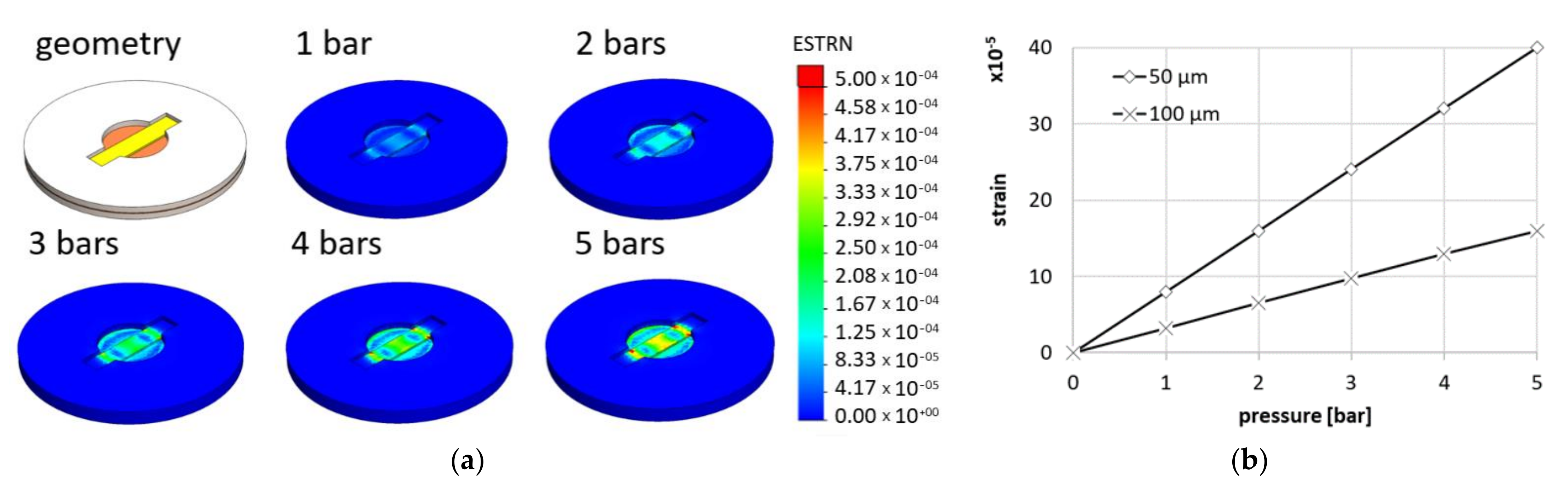
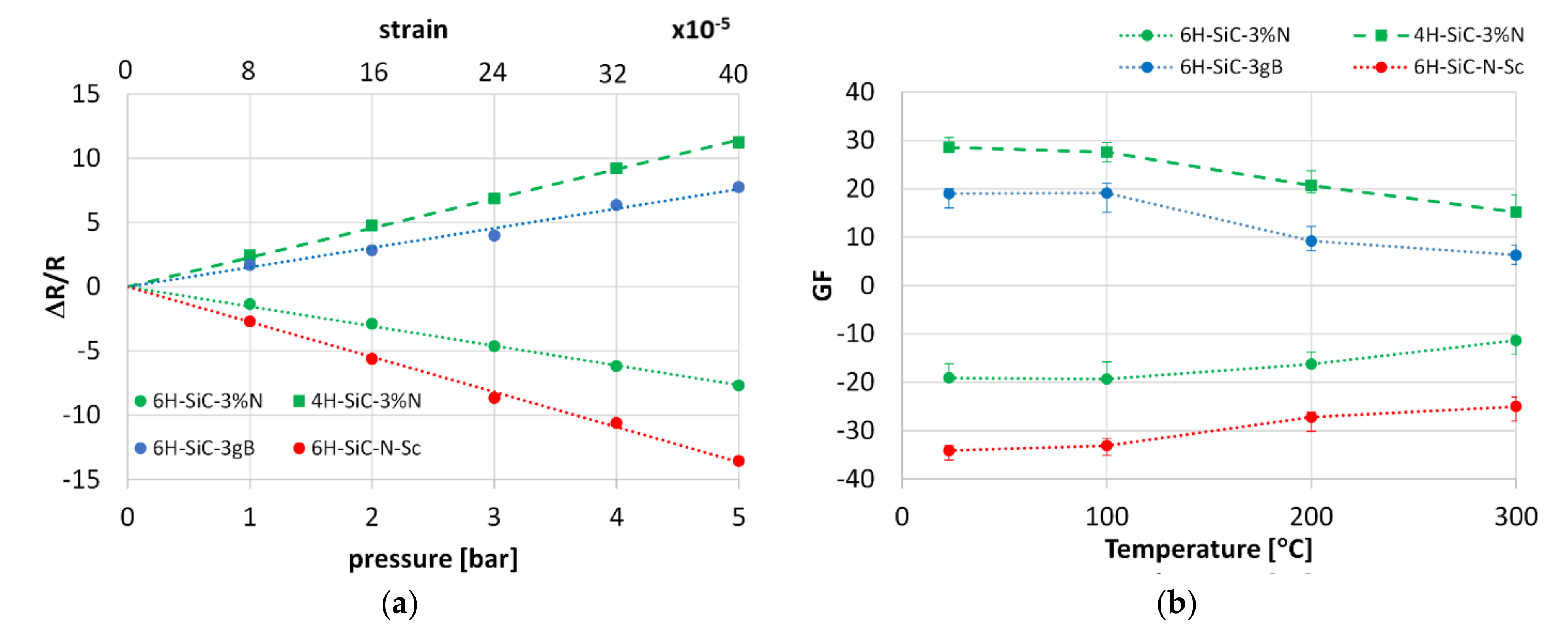
3.2. Pressure Sensor Based on Thin Film Doped SiC
4. Summary and Conclusions
Author Contributions
Funding
Institutional Review Board Statement
Informed Consent Statement
Conflicts of Interest
References
- Thomson, W. On the Electro-Dynamic Qualities of Metals: Effects of Magnetization on the Electric Conductivity of Nickel and of Iron on JSTOR. Proc. R Soc. Lond. 1857, 546–550. Available online: https://www.jstor.org/stable/111415?seq=1#metadata_info_tab_contents (accessed on 18 May 2021).
- Kumar, S.S.; Pant, B.D. Design principles and considerations for the “ideal” silicon piezoresistive pressure sensor: A focused review. Microsyst. Technol. 2014, 20, 1213–1247. [Google Scholar] [CrossRef]
- Toriyama, T.; Sugiyama, S. Analysis of piezoresistance in n-type β-SiC for high-temperature mechanical sensors. Appl. Phys. Lett. 2002, 81, 2797–2799. [Google Scholar] [CrossRef]
- Phan, H.P.; Dao, D.V.; Nakamura, K.; Dimitrijev, S.; Nguyen, N.T. The Piezoresistive Effect of SiC for MEMS Sensors at High Temperatures: A Review. J. Microelectromech. Syst. 2015, 24, 1663–1677. [Google Scholar] [CrossRef] [Green Version]
- Fraga, M.A.; Furlan, H.; Massi, M.; Oliveira, I.C.; Koberstein, L.L. Fabrication and characterization of a SiC/SiO2/Si piezoresistive pressure sensor. Procedia Eng. 2010, 5, 609–612. [Google Scholar] [CrossRef]
- Shor, J.S.; Bemis, L.; Kurtz, A.D. Characterization of Monolithic n-Type 6H-SiC Piezoresistive Sensing Elements. IEEE Trans. Electron. Devices 1994, 41, 661–665. [Google Scholar] [CrossRef]
- Toriyama, T. Piezoresistance consideration on n-type 6H SiC for MEMS-based piezoresistance sensors. J. Micromech. Microeng. 2004, 14, 1445–1448. [Google Scholar] [CrossRef]
- Sarro, P.M. Silicon carbide as a new MEMS technology. Sens. Actuators A Phys. 2000, 82, 210–218. [Google Scholar] [CrossRef]
- Barlian, A.A.; Park, W.T.; Mallon, J.R.; Rastegar, A.J.; Pruitt, B.L. Review: Semiconductor piezoresistance for microsystems. Proc. IEEE 2009, 97, 513–552. [Google Scholar] [CrossRef] [Green Version]
- Mehregany, M.; Zorman, C.A.; Rajan, N.; Wu, C.H. Silicon carbide MEMS for harsh environments. Proc. IEEE 1998, 86, 1594–1609. [Google Scholar] [CrossRef]
- Wright, N.G.; Horsfall, A.B. SiC sensors: A review. J. Phys. D Appl. Phys. 2007, 40, 6345–6354. [Google Scholar] [CrossRef]
- Niu, Z.; Zhao, Y.; Tian, B. Design optimization of high pressure and high temperature piezoresistive pressure sensor for high sensitivity. Rev. Sci. Instrum. 2014, 85. [Google Scholar] [CrossRef] [PubMed]
- Okojie, R.S.; Lukco, D.; Nguyen, V.; Savrun, E. 4H-SiC piezoresistive pressure sensors at 800 °C with observed sensitivity recovery. IEEE Electron. Device Lett. 2015, 36, 174–176. [Google Scholar] [CrossRef]
- Jain, S.; Bhatia, D. A novel design of tactile sensor using piezoresistive cantilever for robotic application. In Proceedings of the 2016 IEEE 7th Power India International Conference (PIICON), Bikaner, India, 25–27 November 2016; Institute of Electrical and Electronics Engineers Inc.: Piscataway, NJ, USA, 2017. [Google Scholar] [CrossRef]
- Rivera, K.; Gregory, O.J. Strain Gages for SiC–SiC Ceramic Matrix Composite Engine Components. IEEE Sens. Lett. 2018, 2, 1–4. [Google Scholar] [CrossRef]
- Boubekri, R.; Cambril, E.; Couraud, L.; Bernardi, L.; Madouri, A.; Portail, M.; Chassagne, T.; Moisson, C.; Zielinski, M.; Jiao, S.; et al. Electrothermally driven high-frequency piezoresistive SiC cantilevers for dynamic atomic force microscopy. J. Appl. Phys. 2014, 116, 54304. [Google Scholar] [CrossRef] [Green Version]
- Xie, H.; Vitard, J.; Haliyo, S.; Régnier, S.; Boukallel, M. Calibration of lateral force measurements in atomic force microscopy with a piezoresistive force sensor. Rev. Sci. Instrum. 2008, 79. [Google Scholar] [CrossRef] [PubMed]
- Tosolini, G.; Villanueva, L.G.; Perez-Murano, F.; Bausells, J. Fast on-wafer electrical, mechanical, and electromechanical characterization of piezoresistive cantilever force sensors. Rev. Sci. Instrum. 2012, 83. [Google Scholar] [CrossRef] [Green Version]
- Tortonese, M.; Barrett, R.C.; Quate, C.F. Atomic resolution with an atomic force microscope using piezoresistive detection. Appl. Phys. Lett. 1993, 62, 834–836. [Google Scholar] [CrossRef]
- Basov, M. High sensitive, linear and thermostable pressure sensor utilizing bipolar junction transistor for 5 kPa. Phys. Scr. 2021, 96, 065705. [Google Scholar] [CrossRef]
- Basov, M. High-sensitivity MEMS pressure sensor utilizing bipolar junction transistor with temperature compensation. Sens. Actuators A Phys. 2020, 303, 111705. [Google Scholar] [CrossRef]
- Tran, A.V.; Zhang, X.; Zhu, B. Mechanical Structural Design of a Piezoresistive Pressure Sensor for Low-Pressure Measurement: A Computational Analysis by Increases in the Sensor Sensitivity. Sensors 2018, 18, 2023. [Google Scholar] [CrossRef] [PubMed] [Green Version]
- Basov, M.; Prigodskiy, D. Development of high-sensitivity piezoresistive pressure sensors for −0.5…+0.5 kPa. J. Micromech. Microeng. 2020, 30, 105006. [Google Scholar] [CrossRef]
- Mackowiak, P.; Schiffer, M.; Xu, X.; Obermeier, E.; Ngo, H. Design and simulation of ultra high sensitive piezoresistive MEMS sensor with structured membrane for low pressure applications. In Proceedings of the 2010 12th Electronics Packaging Technology Conference, Singapore, 8–10 December 2010; pp. 757–761. [Google Scholar] [CrossRef]
- Suzuki, K.; Hasegawa, H.; Kanda, Y. Origin of the linear and nonlinear piezoresistance effects in p-type silicon. Jpn. J. Appl. Phys. 1984, 23, 871–874. [Google Scholar] [CrossRef]
- Phan, H.P.; Kozeki, T.; Dinh, T.; Fujii, T.; Qamar, A.; Zhu, Y.; Namazu, T.; Nguyen, N.T.; Dao, D.V. Piezoresistive effect of p-type silicon nanowires fabricated by a top-down process using FIB implantation and wet etching. RSC. Adv. 2015, 5, 82121–82126. [Google Scholar] [CrossRef] [Green Version]
- Kozlovskiy, S.I.; Sharan, N.N. Piezoresistive effect in p-type silicon classical nanowires at high uniaxial strains. J. Comput. Electron. 2011, 10, 258–267. [Google Scholar] [CrossRef]
- Wang, X.; Zhou, J.; Song, J.; Liu, J.; Xu, N.; Wang, Z.L. Piezoelectric field effect transistor and nanoforce sensor based on a single ZnO nanowire. Nano Lett. 2006, 6, 2768–2772. [Google Scholar] [CrossRef]
- Yang, Y.; Guo, W.; Qi, J.; Zhang, Y. Flexible piezoresistive strain sensor based on single Sb-doped ZnO nanobelts. Appl. Phys. Lett. 2010, 97. [Google Scholar] [CrossRef]
- Yeo, Y.-C.; King, T.-J.; Hu, C. Metal-dielectric band alignment and its implications for metal gate complementary metal-oxide-semiconductor technology. J. Appl. Phys. 2002, 92, 7266–7271. [Google Scholar] [CrossRef] [Green Version]
- Bi, J.; Wei, G.; Shang, M.; Gao, F.; Tang, B.; Yang, W. Piezoresistance in Si3N4 nanobelts: Toward highly sensitive and reliable pressure sensors. J. Mater. Chem. C 2014, 2, 10062–10066. [Google Scholar] [CrossRef]
- Kang, I.; Schulz, M.J.; Kim, J.H.; Shanov, V.; Shi, D. A carbon nanotube strain sensor for structural health monitoring. Smart Mater. Struct. 2006, 15, 737–748. [Google Scholar] [CrossRef]
- Nishio, T.; Miyato, Y.; Kobayashi, K.; Matsushige, K.; Yamada, H. Piezoresistive properties of carbon nanotubes under radial force investigated by atomic force microscopy. Appl. Phys. Lett. 2008, 92. [Google Scholar] [CrossRef] [Green Version]
- Lamba, M.; Chaudhary, H.; Singh, K. Graphene piezoresistive flexible force sensor for harsh condition. In AIP Conference Proceedings; American Institute of Physics Inc.: College Park, MD, USA, 2020; Volume 2294, p. 020008. [Google Scholar] [CrossRef]
- Nag, M.; Kumar, A.; Singh, K.; Pratap, B. Graphene based flexible piezoresistive pressure sensor for electric vehicles applications. In AIP Conference Proceedings; American Institute of Physics Inc.: College Park, MD, USA, 2020; Volume 2294. [Google Scholar] [CrossRef]
- Zhu, S.E.; Krishna Ghatkesar, M.; Zhang, C.; Janssen, G.C.A.M. Graphene based piezoresistive pressure sensor. Appl. Phys. Lett. 2013, 102. [Google Scholar] [CrossRef] [Green Version]
- Kimoto, T.; Cooper, J.A. Fundamentals of Silicon Carbide Technology: Growth, Characterization, Devices and Application; John Wiley & Sons: Hoboken, NJ, USA, 2014; Volume 9781118313. [Google Scholar] [CrossRef]
- Wright, N.G.; Horsfall, A.B.; Vassilevski, K. Prospects for SiC electronics and sensors. Mater. Today 2008, 11, 16–21. [Google Scholar] [CrossRef]
- Jiang, L.; Cheung, R. A review of silicon carbide development in MEMS applications. Int. J. Comput. Mater. Sci. Surf. Eng. 2009, 2, 227–242. [Google Scholar] [CrossRef] [Green Version]
- Baliga, B.J. Silicon Carbide Power Devices; World Scientific: Singapore, 2006. [Google Scholar] [CrossRef]
- Akiyama, T.; Briand, D.; De Rooij, N.F. Design-dependent gauge factors of highly doped n-type 4H-SiC piezoresistors. J. Micromech. Microeng. 2012, 22. [Google Scholar] [CrossRef]
- Okojie, R.S.; Ned, A.A.; Kurtz, A.D.; Carr, W.N. Characterization of highly doped n- and p-type 6H-SiC piezoresistors. IEEE Trans. Electron. Devices 1998, 45, 785–790. [Google Scholar] [CrossRef]
- Shor, J.S.; Goldstein, D.; Kurtz, A.D. Characterization of n-Type β-SiC as a Piezoresistor. IEEE Trans. Electron. Devices 1993, 40, 1093–1099. [Google Scholar] [CrossRef]
- Wu, C.H.; Zorman, C.A.; Mehregany, M. Fabrication and testing of bulk micromachined silicon carbide piezoresistive pressure sensors for high temperature applications. IEEE Sens. J. 2006, 6, 316–323. [Google Scholar] [CrossRef]
- Yasui, K.; Miura, H.; Takata, M.; Akahane, T. SiCOI structure fabricated by catalytic chemical vapor deposition. Thin Solid Film. 2008, 516, 644–647. [Google Scholar] [CrossRef]
- Eickhoff, M.; Stutzmann, M. Influence of crystal defects on the piezoresistive properties of 3C-SiC. J. Appl. Phys. 2004, 96, 2878–2888. [Google Scholar] [CrossRef]
- Strass, J.; Eickhoff, M.; Kroetz, G. Influence of crystal quality on the piezoresistive effect of β-SiC between RT and 450 °C measured by using microstructures. In International Conference Solid State Sensors Actuators Proceedings, Chicago, IL, USA, 19 June 1997; IEEE: Piscataway, NJ, USA, 1997; Volume 2, pp. 1439–1442. [Google Scholar] [CrossRef]
- Phan, H.P.; Viet Dao, D.; Tanner, P.; Wang, L.; Nguyen, N.T.; Zhu, Y.; Dimitrijev, S. Fundamental piezoresistive coefficients of p-type single crystalline 3C-SiC. Appl. Phys. Lett. 2014, 104. [Google Scholar] [CrossRef]
- Phan, H.P.; Dao, D.V.; Tanner, P.; Han, J.; Nguyen, N.T.; Dimitrijev, S.; Walker, G.; Wang, L.; Zhu, Y. Thickness dependence of the piezoresistive effect in p-type single crystalline 3C-SiC nanothin films. J. Mater. Chem. C 2014, 2, 7176–7179. [Google Scholar] [CrossRef] [Green Version]
- Phan, H.P.; Dinh, T.; Kozeki, T.; Qamar, A.; Namazu, T.; Dimitrijev, S.; Nguyen, N.T.; Dao, D.V. Piezoresistive effect in p-Type 3C-SiC at high temperatures characterized using Joule heating. Sci. Rep. 2016, 6, 1–9. [Google Scholar] [CrossRef]
- Eickhoff, M.; Möller, M.; Kroetz, G.; Stutzmann, M. Piezoresistive properties of single crystalline, polycrystalline, and nanocrystalline n-type 3C-SiC. J. Appl. Phys. 2004, 96, 2872–2877. [Google Scholar] [CrossRef]
- Homma, T.; Kamimura, K.; Cai, H.Y.; Onuma, Y. Preparation of polycrystalline SiC films for sensors used at high temperature. Sens. Actuators A Phys. 1994, 40, 93–96. [Google Scholar] [CrossRef]
- Phan, H.P.; Dao, D.V.; Wang, L.; Dinh, T.; Nguyen, N.T.; Qamar, A.; Tanner, P.; Dimitrijev, S.; Zhu, Y. The effect of strain on the electrical conductance of p-type nanocrystalline silicon carbide thin films. J. Mater. Chem. C 2015, 3, 1172–1176. [Google Scholar] [CrossRef] [Green Version]
- Fraga, M.A.; Massi, M.; Furlan, H.; Oliveira, I.C.; Rasia, L.A.; Mateus, C.F.R. Preliminary evaluation of the influence of the temperature on the performance of a piezoresistive pressure sensor based on a-SiC film. Microsyst. Technol. 2011, 17, 477–480. [Google Scholar] [CrossRef]
- Fraga, M.A.; Furlan, H.; Pessoa, R.S.; Rasia, L.A.; Mateus, C.F.R. Studies on SiC, DLC and TiO2 thin films as piezoresistive sensor materials for high temperature application. Microsyst. Technol. 2012, 18, 1027–1033. [Google Scholar] [CrossRef]
- Kim, K.J.; Lim, K.Y.; Kim, Y.W.; Kim, H.C. Temperature Dependence of Electrical Resistivity (4–300 K) in Aluminum- and Boron-Doped SiC Ceramics. J. Am. Ceram. Soc. 2013, 96, 2525–2530. [Google Scholar] [CrossRef]
- Ser, C.T.; Mak, A.M.; Wejrzanowski, T.; Tan, T.L. Designing piezoresistive materials from first-principles: Dopant effects on 3C-SiC. Comput. Mater. Sci. 2021, 186, 110040. [Google Scholar] [CrossRef]
- Matsunami, H.; Kimoto, T. Step-controlled epitaxial growth of SiC: High quality homoepitaxy. Mater. Sci. Eng. R Rep. 1997, 20, 125–166. [Google Scholar] [CrossRef]
- Tymicki, E.; Grasza, K.; Racka, K.; Łukasiewicz, T.; Piersa, M.; Kościewicz, K.; Teklińska, D.; Diduszko, R.; Skupiński, P.; Jakieła, R.; et al. Effect of nitrogen doping on the growth of 4H polytype on the 6H-SiC seed by PVT method. In Materials Science Forum; Trans Tech Publications Ltd.: Freienbach, Switzerland, 2012; Volume 717–720, pp. 29–32. [Google Scholar] [CrossRef]
- Phan, H.P.; Dinh, T.; Kozeki, T.; Nguyen, T.K.; Qamar, A.; Namazu, T.; Nguyen, N.T.; Dao, D.V. The Piezoresistive Effect in Top-Down Fabricated p-Type 3C-SiC Nanowires. IEEE Electron. Device Lett. 2016, 37, 1029–1032. [Google Scholar] [CrossRef]
- Rowe, A.C.H. Piezoresistance in silicon and its nanostructures. J. Mater. Res. 2014, 29, 731–744. [Google Scholar] [CrossRef] [Green Version]
- Tymicki, E.; Grasza, K.; Racka, K.; Raczkiewicz, M.; Łukasiewicz, T.; Gała, M.; Kościewicz, K.; Diduszko, R.; Bożek, R. Growth of 4H-SiC Single Crystals on 6H-SiC Seeds with an Open Backside by PVT Method. Mater. Sci. Forum 2009, 615–617, 15–18. [Google Scholar] [CrossRef]
- Nakashima, S.; Harima, H. Characterization of Defects in SiC Crystals by Raman Scattering. In Silicon Carbide; Springer: Berlin, Heidelberg, 2004; pp. 585–605. [Google Scholar] [CrossRef]
- Phan, H.P.; Tanner, P.; Dao, D.V.; Wang, L.; Nguyen, N.T.; Zhu, Y.; Dimitrijev, S. Piezoresistive effect of p-type single crystalline 3C-SiC thin film. IEEE Electron. Device Lett. 2014, 35, 399–401. [Google Scholar] [CrossRef] [Green Version]
- Iwata, H.; Itoh, K.M. Donor and acceptor concentration dependence of the electron Hall mobility and the Hall scattering factor in n-type 4H– and 6H–SiC. J. Appl. Phys. 2001, 89, 6228. [Google Scholar] [CrossRef] [Green Version]
- Li, X.B.; Chen, Z.Z.; Shi, E.W. Effect of doping on the Raman scattering of 6H-SiC crystals. Phys. B Condens. Matter 2010, 405, 2423–2426. [Google Scholar] [CrossRef]
- Dao, D.V.; Phan, H.P.; Qamar, A.; Dinh, T. Piezoresistive effect of p-type single crystalline 3C-SiC on (111) plane. RSC Adv. 2016, 6, 21302–21307. [Google Scholar] [CrossRef] [Green Version]
- Nguyen, T.K.; Phan, H.P.; Han, J.; Dinh, T.; Foisal, A.R.M.; Dimitrijev, S.; Zhu, Y.; Nguyen, N.T.; Dao, D.V. Highly sensitive p-Type 4H-SiC van der Pauw sensor. RSC Adv. 2018, 8, 3009–3013. [Google Scholar] [CrossRef] [Green Version]
- Wei, J.; Magnani, S.; Sarro, P.M. Suspended submicron silicon-beam for high sensitivity piezoresistive force sensing cantilevers. Sens. Actuators A Phys. 2012, 186, 80–85. [Google Scholar] [CrossRef]
- Belwanshi, V.; Topkar, A. Quantitative analysis of temperature effect on SOI piezoresistive pressure sensors. Microsyst. Technol. 2017, 23, 2719–2725. [Google Scholar] [CrossRef]
- Mohammed, A.; Moussa, W.A.; Lou, E. High Sensitivity MEMS Strain Sensor: Design and Simulation. Sensors 2008, 8, 2642–2661. [Google Scholar] [CrossRef] [PubMed] [Green Version]
- Kulha, P.; Babchenko, O.; Kromka, A.; Husaka, M.; Haenen, K. Design and fabrication of piezoresistive strain gauges based on nanocrystalline diamond layers. Vacuum 2012, 86, 689–692. [Google Scholar] [CrossRef]


| Polytype | Dopant Type/Element | Growth | Carrier Concentration | Gauge Factor | Orientation | Stress | |
|---|---|---|---|---|---|---|---|
| Room Temp | High Temp | ||||||
| Single 4H-SiC [41] | n/N | - | 1.5 × 10¹⁹ | 20.8 | - | (0001) | uniaxial |
| Single 6H-SiC [6] | n/N | - | 3.8 × 10¹⁸ | −29.4 | −17 (250 °C) | (0001) | uniaxial |
| Single 6H-SiC [42] | n/N | - | 2 × 10¹⁹ | −22 | −11 (250 °C) | (0001) | uniaxial |
| Single 6H-SiC [42] | p/Al | - | 2 × 10¹⁹ | 27 | 12 (250 °C) | (0001) | uniaxial |
| Single 3C-SiC [43] | n/N | APCVD | 1018 | −31.8 | −18 (450 °C) | [100] | uniaxial |
| Single 3C-SiC [44] | n/N | HMCVD | 1018 | −27 | - | [100] | uniaxial |
| Single 3C-SiC [45] | n/N | APCVD | - | −18 | −7 (400 °C) | [100] | biaxial |
| Single 3C-SiC [46] | n/N | LPCVD | 0.4–2 × 10¹⁹ | −24.8 | −11 (450 °C) | [100] | biaxial |
| Single 3C-SiC [47] | n/N | APCVD | highly doped | −16 | −12.5 (400 °C) | [100] | uniaxial |
| Single 3C-SiC [48] | p/Al | LPCVD | 5 × 10¹⁸ | 30.3 | - | [110] | uniaxial |
| Single 3C-SiC [49] | p/Al | LPCVD | 1.3–10 × 1018 | 20–30 | - | [110] | uniaxial |
| Single 3C-SiC [50] | p/Al | LPCVD | highly doped | 28 | 25 (300 °C) | [110] | uniaxial |
| Poly 3C-SiC [51] | n/N | LPCVD | low doped | −10 | - | - | biaxial |
| Poly 3C-SiC [44] | n/N | LPCVD | - | −2.1 | - | - | biaxial |
| Poly 3C-SiC [52] | p/B | LPCVD | 1018–1020 | 10 | 7 (200 °C) | - | uniaxial |
| Nanocrystalline SiC [53] | p/Al | LPCVD | 2 × 10¹⁸ | 14.5 | - | - | uniaxial |
| Amorphous SiC [54,55] | n/N | PECVD | - | 49 | - | - | uniaxial |
| n/N | Sputtering | - | 31 | - | - | uniaxial | |
| Sample | n [cm−3] | ρ [Ωcm] | µ [cm2/Vs] | Type | GF |
|---|---|---|---|---|---|
| 4H 0%N | 5.64 × 10¹⁷ | 4.64 × 10⁻² | 2.38 × 10² | n | 2.1 ± 0.4 |
| 4H 3%N | 5.00 × 10¹⁸ | 1.60 × 10⁻² | 7.78 × 101 | n | 6.4 ± 2.5 |
| 4H 10%N | 9.28 × 10¹⁸ | 1.16 × 10⁻² | 5.81 × 101 | n | 4.8 ± 1.3 |
| 6H 0%N | 2.34 × 10¹⁶ | 8.78 × 10⁻¹ | 2,12 × 10² | n | −1.2 ± 0.3 |
| 6H 3%N | 1.28 × 10¹⁸ | 3.82 × 10⁻² | 1.28 × 10² | n | −5.8 ± 2.3 |
| 6H 10%N | 6.15 × 10¹⁸ | 1.85 × 10⁻² | 5.49 × 101 | n | −2.8 ± 0.7 |
| 6H B 1g | 1.08 × 10¹⁶ | 2.39 × 10⁻¹ | 2.41 × 101 | p | 4.4 ± 1.6 |
| 6H B 3g | 4.12 × 10¹⁷ | 3.34 × 10⁻² | 1.28 × 101 | p | 4.6 ± 1.4 |
| 6H N Sc | 4.60 × 10¹⁸ | 1.81 × 10⁻² | 6.12 × 101 | n | 7.2 ± 2.6 |
Publisher’s Note: MDPI stays neutral with regard to jurisdictional claims in published maps and institutional affiliations. |
© 2021 by the authors. Licensee MDPI, Basel, Switzerland. This article is an open access article distributed under the terms and conditions of the Creative Commons Attribution (CC BY) license (https://creativecommons.org/licenses/by/4.0/).
Share and Cite
Wejrzanowski, T.; Tymicki, E.; Plocinski, T.; Bucki, J.J.; Tan, T.L. Design of SiC-Doped Piezoresistive Pressure Sensor for High-Temperature Applications. Sensors 2021, 21, 6066. https://doi.org/10.3390/s21186066
Wejrzanowski T, Tymicki E, Plocinski T, Bucki JJ, Tan TL. Design of SiC-Doped Piezoresistive Pressure Sensor for High-Temperature Applications. Sensors. 2021; 21(18):6066. https://doi.org/10.3390/s21186066
Chicago/Turabian StyleWejrzanowski, Tomasz, Emil Tymicki, Tomasz Plocinski, Janusz Józef Bucki, and Teck Leong Tan. 2021. "Design of SiC-Doped Piezoresistive Pressure Sensor for High-Temperature Applications" Sensors 21, no. 18: 6066. https://doi.org/10.3390/s21186066
APA StyleWejrzanowski, T., Tymicki, E., Plocinski, T., Bucki, J. J., & Tan, T. L. (2021). Design of SiC-Doped Piezoresistive Pressure Sensor for High-Temperature Applications. Sensors, 21(18), 6066. https://doi.org/10.3390/s21186066