
An Instrument for the Characterization and Calibration of Optical Sensors


 , ,
, , 

Abstract
:1. Introduction
- -
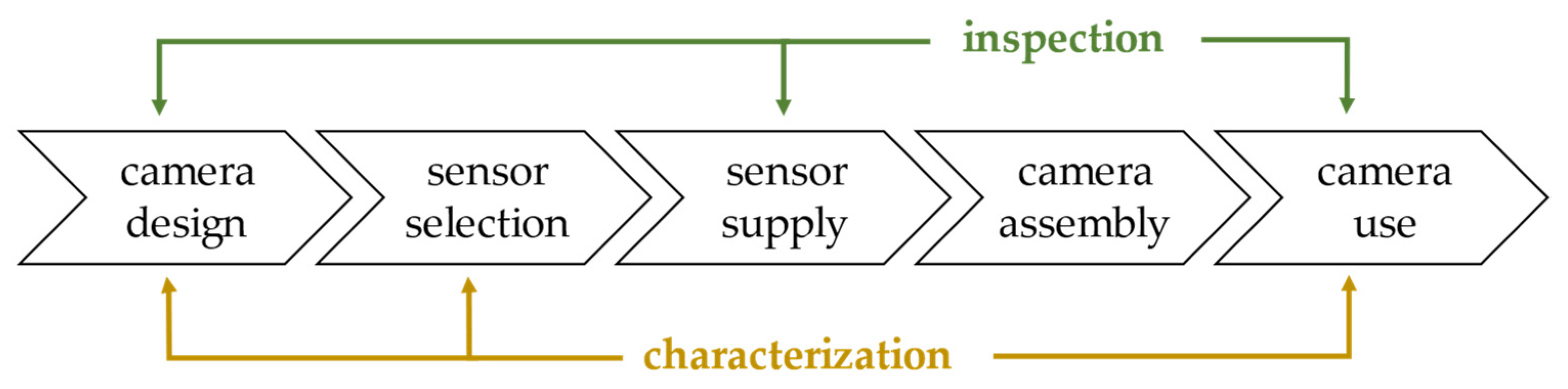
- As an individual component during the sensor manufacturing for process control or before delivery.
- -
- During the manufacturing of the integrated product (e.g., industrial, professional, mobile cameras), after supply by acceptance testing or sampling, at various assembly stages, and final testing.
- -
- By the system integrator (e.g., a vision system or an optical instrument) for the firmware/software development and the final testing of the integrated system.
- -
- By the final user (e.g., a factory or a laboratory) for setup, maintenance, and periodic calibration.
1.1. Literature
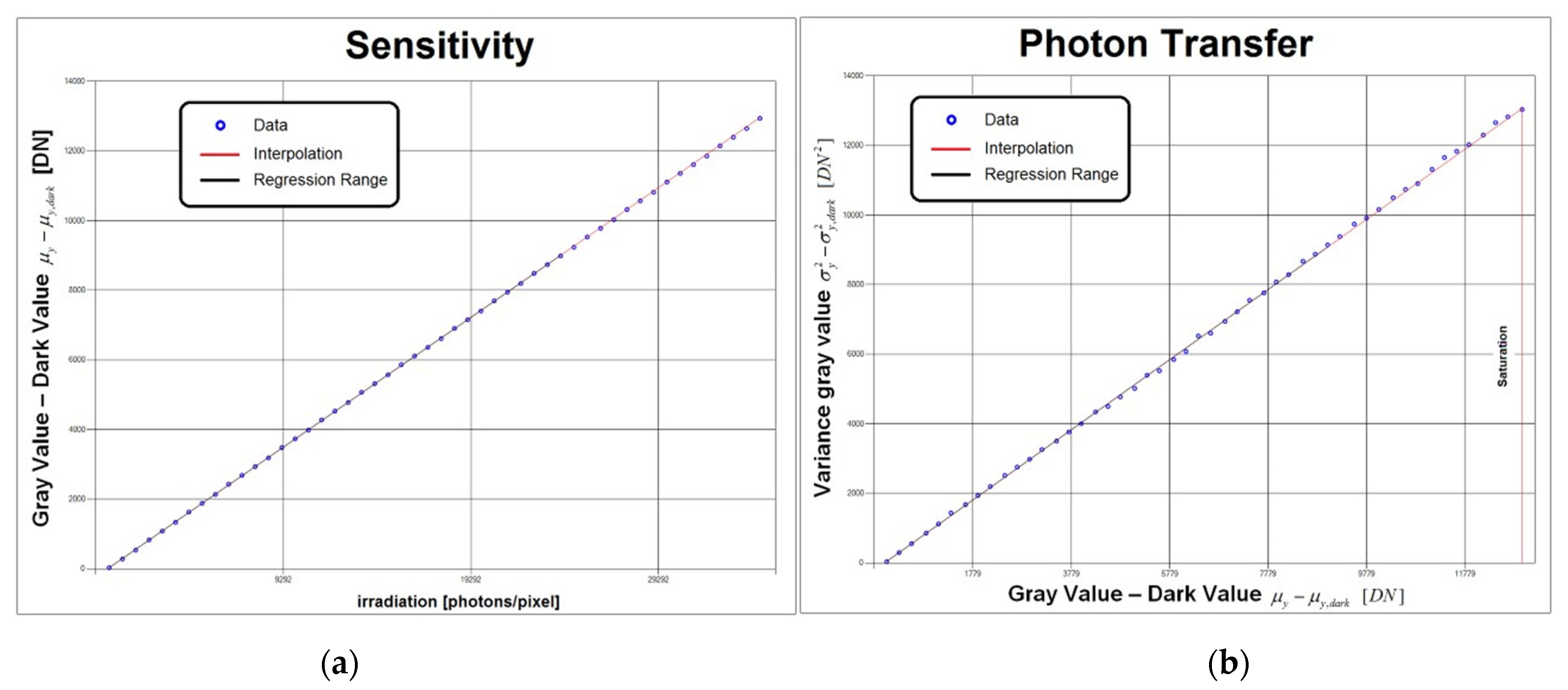
1.2. EMVA 1288 Standard
- -
- The sensor is linear, i.e., the digital output signal increases linearly with the number of photons.
- -
- The number of photons collected by a pixel depends on the product of irradiance E (units W/m2) and exposure time texp (units s), i.e., the radiative energy density E*texp at the sensor plane.
- -
- All noise sources are wide sense stationary and white concerning time and space. In other words, the parameters describing the noise are invariant with respect to time and space.
- -
- Only the total quantum efficiency is wavelength dependent. Therefore, the effects caused by light of different wavelengths can be linearly superimposed.
- -
- Only the dark current is temperature dependent.
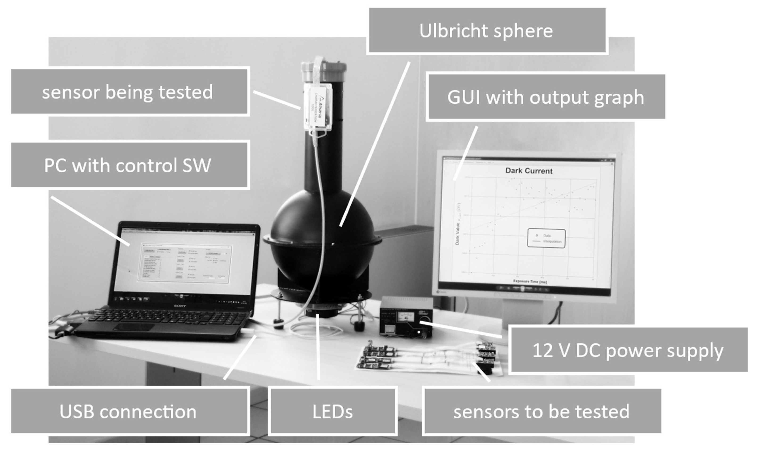
2. Development of the Proposed Instrument
- -
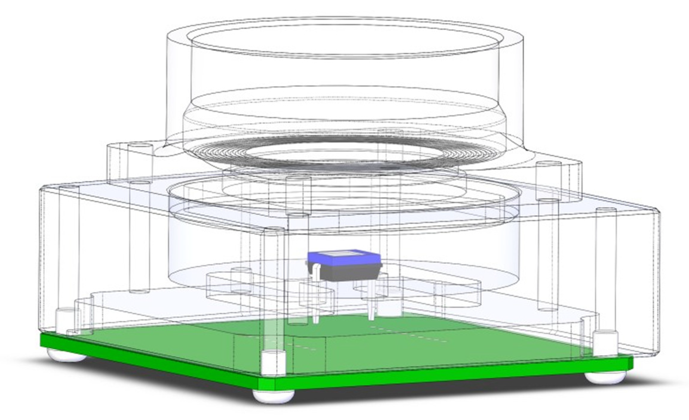
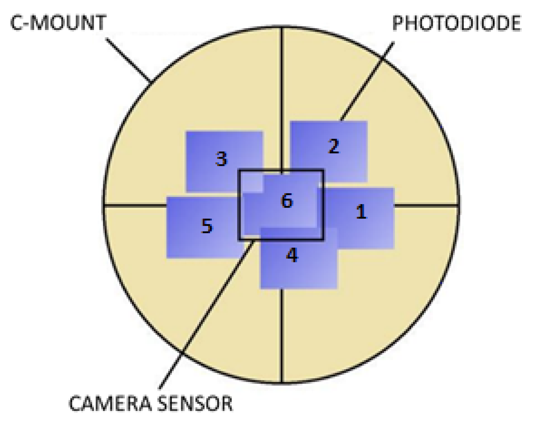
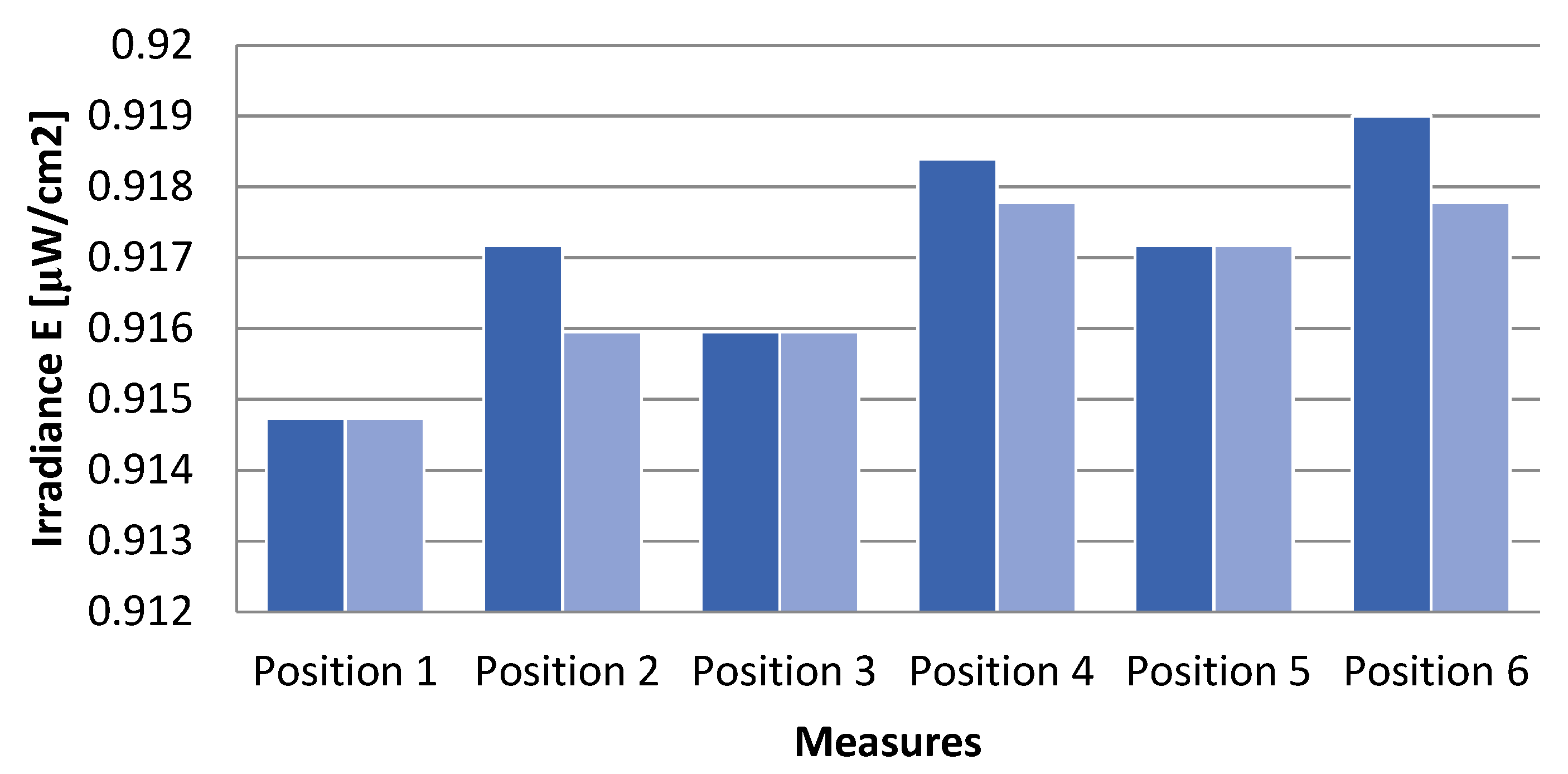
- Sphere (Figure 2: ①–②): diffuses the light internally. Only the light rays perpendicular to the sensitive surface of the camera at the top of the tube (Figure 2: ⑪) can reach the sensor because the tube is coated internally with a non reflective material. More details are provided in Section 2.1. The experimental method to evaluate the light uniformity measurement is described in Section 4.
- -
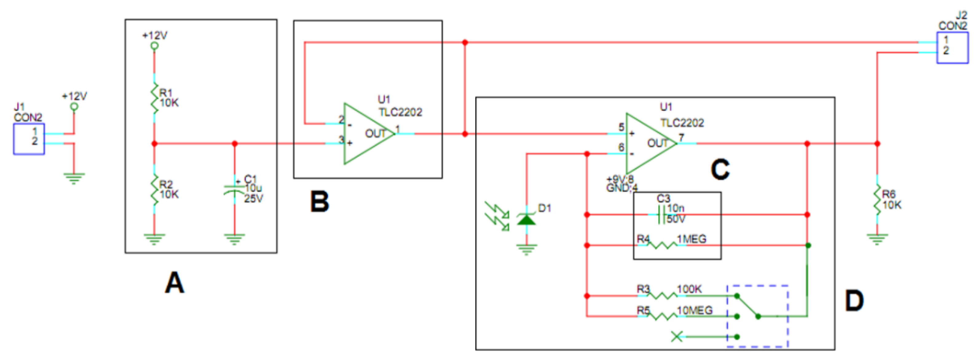
- Photodiode circuit (Figure 2: ⑬) to be inserted in the place of the camera to be tested to measure the number of photons reaching the sensor plane (detailed in Section 2.2).
- -
- Illuminator with three Red, Green, and Blue (RGB) LEDs controlled via an FT232BL chip converting Universal Serial Bus (USB) to RS232 serial connection from the PC, detailed in (Section 2.3). The LEDs are placed in the lower part of the sphere (Figure 2: ⑨), opposite the sensor and thermally regulated by an air cooling system (Figure 2: ⑩).
- -
- Control software on a Personal Computer (PC): controls the on/off switching of the individual LEDs of the illuminator, receives the grabbed images, processes images, and provides a report with numerical information, including the graphs required by the EMVA 1288 standard tests (Section 2.4).
2.1. Sphere
2.2. Photodiode
2.3. Illuminator
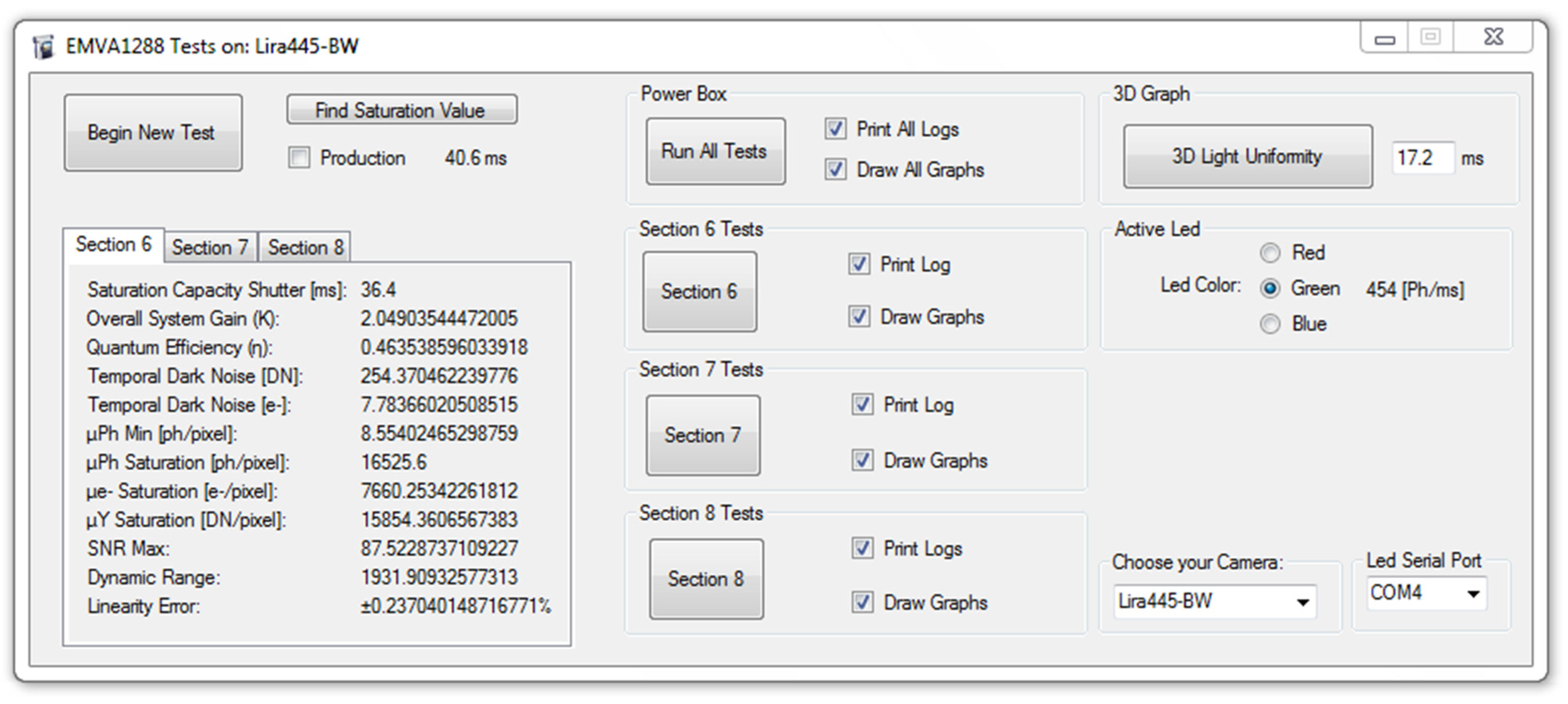
2.4. Control Software
- The camera characterization requires many samples, allowing accurate evaluation of the camera properties.
- The inspection mode is used in production with lower testing time.
3. Experimental
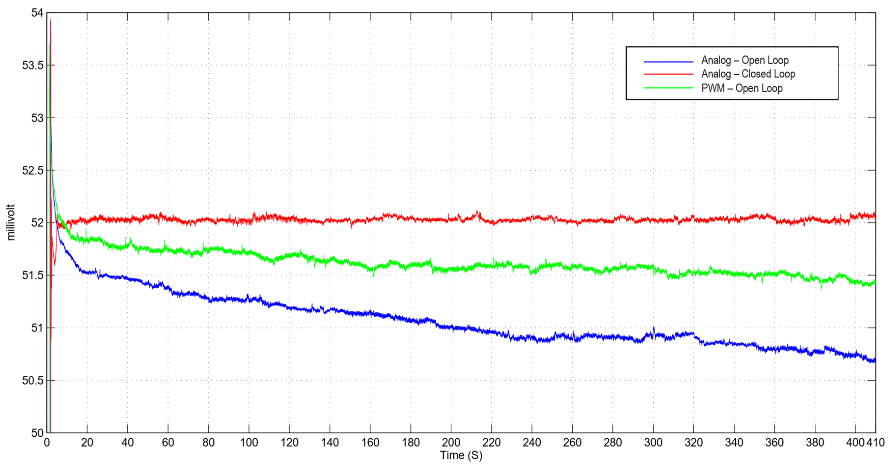
- -
- it is more efficient from a thermal point of view thanks to the digital components that require less power;
- -
- the system has simpler components than the analog board;
- -
- it can be easily controlled remotely.
4. Instrument Validation Method
5. Conclusions
- -
- A calibration procedure for verifying the effects of hardware and software changes of the camera in real time. This can be achieved using an iterative testing method in the design phase that allows tweaking the hardware by quickly converging towards an optimal solution.
- -
- Using a real radiometer instead of the Vishay photodiode would allow the certification of the results produced and greater accuracy in detecting the number of photons incident on the sensor.
- -
- Extending the spectral analysis using a series of LEDs at different wavelengths or a broad spectrum illuminator with a bank of filters at set wavelengths, particularly for color sensors.
- -
- Addition of a temperature sensor and control to increase the instrument productivity, speed up the LED warming, and prevent the risk of overheating. This would also allow characterizing the dependence of the dark current on the temperature.
- -
- Scaling the instrument in size by a modular design accommodates the downsizing of sensors, e.g., by additive manufacturing for design and part replacement flexibility and checking the potential effect of geometric accuracy [24].
Author Contributions
Funding
Institutional Review Board Statement
Informed Consent Statement
Data Availability Statement
Acknowledgments
Conflicts of Interest
References
- Radhakrishna, M.V.V.; Govindh, M.V.; Krishna Veni, P. A Review on Image Processing Sensor. J. Phys. Conf. Ser. 2021, 1714, 12055. [Google Scholar] [CrossRef]
- Pirzada, M.; Altintas, Z. Recent progress in optical sensors for biomedical diagnostics. Micromachines 2020, 11, 356. [Google Scholar] [CrossRef] [PubMed] [Green Version]
- Mehta, S.; Patel, A.; Mehta, J. CCD or CMOS Image sensor for photography. In Proceedings of the 2015 International Conference on Communication and Signal Processing (ICCSP 2015), Melmaruvathur, India, 2–4 April 2015; Institute of Electrical and Electronics Engineers Inc.: Piscataway, NJ, USA, 2015; pp. 291–294. [Google Scholar] [CrossRef]
- Dittrich, P.-G.; Bichra, M.; Stiehler, D.; Pfützenreuter, C.; Radtke, L.; Rosenberger, M.; Notni, G. Extended characterization of multispectral resolving filter-on-chip snapshot-mosaic CMOS cameras. SPIE 2019, 10986, 17. [Google Scholar] [CrossRef]
- Valencia-Jimenez, N.; Leal-Junior, A.; Avellar, L.; Vargas-Valencia, L.; Caicedo-Rodríguez, P.; Ramírez-Duque, A.A.; Lyra, M.; Marques, C.; Bastos, T.; Frizera, A. A Comparative Study of Markerless Systems Based on Color-Depth Cameras, Polymer Optical Fiber Curvature Sensors, and Inertial Measurement Units: Towards Increasing the Accuracy in Joint Angle Estimation. Electronics 2019, 8, 173. [Google Scholar] [CrossRef] [Green Version]
- Bisti, F.; Alexeev, I.; Lanzetta, M.; Schmidt, M. A simple laser beam characterization apparatus based on imaging. J. Appl. Res. Technol. 2021, 19, 98–116. [Google Scholar] [CrossRef]
- Ljung, L. System Identification. In Wiley Encyclopedia of Electrical and Electronics Engineering; John Wiley & Sons, Inc.: Hoboken, NJ, USA, 2017; pp. 1–19. [Google Scholar] [CrossRef]
- EMVA. Standard 1288 Standard for Characterization of Image Sensors and Cameras; EMVA: Barcelona, Spain, 2016. [Google Scholar]
- HOME—Alkeria Machine Vision Cameras. Available online: https://www.alkeria.com/it/ (accessed on 9 June 2021).
- Rosenberger, M.; Zhang, C.; Votyakov, P.; Preißler, M.; Celestre, R.; Notni, G. EMVA 1288 Camera characterisation and the influences of radiometric camera characteristics on geometric measurements. Acta IMEKO 2016, 5, 81–87. [Google Scholar] [CrossRef] [Green Version]
- Wong, K.Y.K.; Zhang, G.; Chen, Z. A stratified approach for camera calibration using spheres. IEEE Trans. Image Process. 2011, 20, 305–316. [Google Scholar] [CrossRef] [PubMed] [Green Version]
- Sun, J.; Chen, X.; Gong, Z.; Liu, Z.; Zhao, Y. Accurate camera calibration with distortion models using sphere images. Opt. Laser Technol. 2015, 65, 83–87. [Google Scholar] [CrossRef]
- Lanzetta, M.; Culpepper, M.L. Integrated visual nanometric three-dimensional positioning and inspection in the automated assembly of AFM probe arrays. CIRP Ann.Manuf. Technol. 2010, 59, 13–16. [Google Scholar] [CrossRef] [Green Version]
- Ducharme, A.; Daniels, A.; Grann, E.; Boreman, G. Design of an integrating sphere as a uniform illumination source. IEEE Trans. Educ. 1997, 40, 131–134. [Google Scholar] [CrossRef]
- Carr, K.F. Integrating Sphere Theory and Applications. Surf. Coat. Int. 2017, 80, 380–385. [Google Scholar] [CrossRef]
- Feng, W.; He, Y.; Shi, F.G. Investigation of LED light output performance characteristics under different alternating current regulation modes. IEEE J. Sel. Top. Quantum Electron. 2011, 17, 720–723. [Google Scholar] [CrossRef]
- Liao, T.J.; Chen, C.L. Robust LED backlight driver with low output voltage drop and hig output current accuracy. In Proceedings of the 2008 IEEE International Conference on Sustainable Energy Technologies (ICSET 2008), Singapore, 24–27 November 2008; pp. 63–66. [Google Scholar] [CrossRef]
- Oh, I.H. An analysis of current accuracies in peak and hysteretic current controlled power LED drivers. In Proceedings of the Conference Proceedings—IEEE Applied Power Electronics Conference and Exposition (APEC), Austin, TX, USA, 24–28 February 2008; pp. 572–577. [Google Scholar] [CrossRef]
- Radtke, L.; Notni, G.; Rosenberger, M.; Graf-Batuchtin, I. Adaptive test bench for characterizing image processing sensors. SPIE 2018, 10656, 62. [Google Scholar] [CrossRef]
- Ritt, G.; Schwarz, B.; Eberle, B. Estimation of Lens Stray Light with Regard to the Incapacitation of Imaging Sensors. Sensors 2020, 20, 6308. [Google Scholar] [CrossRef] [PubMed]
- Camera and Sensor Measuring—Digital Image Processing. Available online: https://www.aeon.de/camera_sensormeasuring.html#Services (accessed on 20 July 2021).
- BPW34, BPW34S Silicon PIN Photodiode|Vishay. Available online: https://www.vishay.com/product?docid=81521 (accessed on 16 June 2021).
- TLC2202 Data Sheet, Product Information. Available online: https://www.ti.com/product/TLC2202 (accessed on 16 June 2021).
- Rossi, A.; Chiodi, S.; Lanzetta, M. Minimum Centroid Neighborhood for Minimum Zone Sphericity. Precis. Eng. 2014, 38, 337–347. [Google Scholar] [CrossRef]


| Data | Symbol | Typical | DevStd | Quantity |
|---|---|---|---|---|
| Quantum Efficiency 1,2 | η | 37.55 | 0.52 | % |
| System Gain Inverse | 1/K | 1.0034 | 0.0149 | e−/DN |
| Inverse of Photon Transfer | 1/ηK | 2.67 | 0.02 | p~/DN |
| Temporal Dark Noise | 157 | 24 | DN2 | |
| 12.57 | 1.12 | e− | ||
| Dark Signal Non Uniformity | DSNU1288 | 0.8337 | 0.59 | DN |
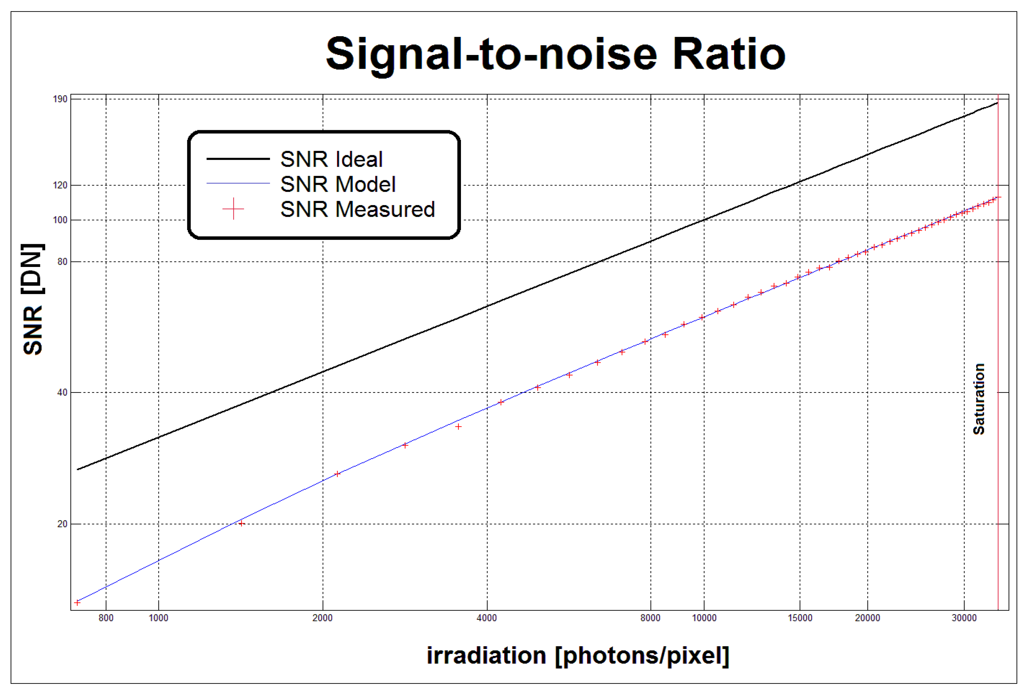
| Maximum achievable SNR 3 | SNRmax | 121.2 | 0.88 | DN |
| 41.67 | 0.06 | dB | ||
| 6.92 | 0.01 | bit | ||
| Inverse of Max Achievable SNR | SNRmax−1 | 0.825 | 0.006 | % |
| Photo Response Non Uniformity | PRNU1288 | 0.1966 | 0.04 | % |
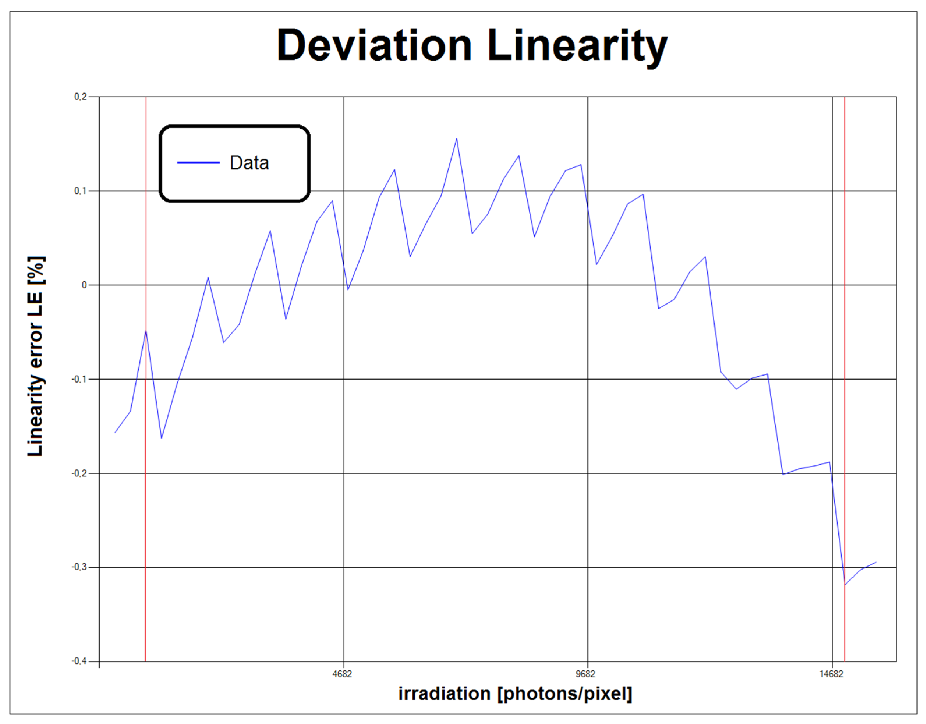
| Non Linearity Error | LE | ±0.253 | 0.036 | % |
| Absolute Sensitivity Limit 1 | µe,min | 6.3 | 0.2 | e− |
| µp,min | 16.75 | 0.379 | p~ | |
| Saturation Capability 1 | µe,sat | 14688 | 212 | e− |
| Saturation Irradiance 1 | µp,sat | 39117 | 354 | p~ |
| Dynamic Range | 2336 | 65.14 | DN | |
| 67.37 | 0.24 | dB | ||
| DRbit | 11.19 | 0.04 | bit | |
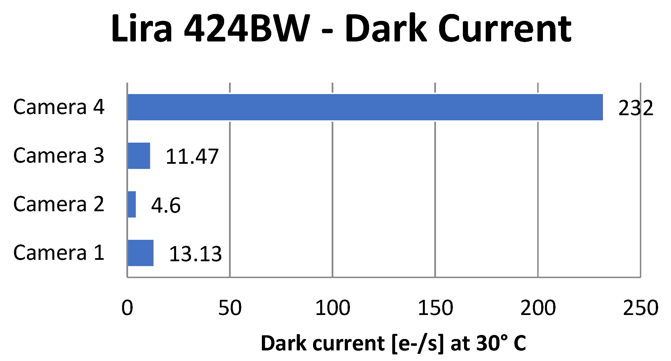
| Dark Current | 63 | 108 | DN/s | |
| 65 | 111 | e−/s |
| Parameters | Alkeria Lira 424 BW | Basler scA640-70 gm |
|---|---|---|
| Temporal Dark Noise σd | 12.57 [e−] | 11 [e−] |
| Saturation Capacity | 14688 [e−] | 14000 [e−] |
| Absolute Sensitivity Limit | 16.75 p~ | 25 p~ |
| Dynamic Range | 11.19 bit | 10.3 bit |
| SNRmax | 41.67 dB | 41.6 dB |
| DSNU1288 | 0.8365 [DN] | 2.9 [DN] |
| PRNU1288 | 0.1966% | 0.5% |
Publisher’s Note: MDPI stays neutral with regard to jurisdictional claims in published maps and institutional affiliations. |
© 2021 by the authors. Licensee MDPI, Basel, Switzerland. This article is an open access article distributed under the terms and conditions of the Creative Commons Attribution (CC BY) license (https://creativecommons.org/licenses/by/4.0/).
Share and Cite
Gastasini, E.; Capecci, N.; Lupi, F.; Gagliardi, A.; Saponara, S.; Lanzetta, M. An Instrument for the Characterization and Calibration of Optical Sensors. Sensors 2021, 21, 5141. https://doi.org/10.3390/s21155141
Gastasini E, Capecci N, Lupi F, Gagliardi A, Saponara S, Lanzetta M. An Instrument for the Characterization and Calibration of Optical Sensors. Sensors. 2021; 21(15):5141. https://doi.org/10.3390/s21155141
Chicago/Turabian StyleGastasini, Enrico, Niccolò Capecci, Francesco Lupi, Alessio Gagliardi, Sergio Saponara, and Michele Lanzetta. 2021. "An Instrument for the Characterization and Calibration of Optical Sensors" Sensors 21, no. 15: 5141. https://doi.org/10.3390/s21155141
APA StyleGastasini, E., Capecci, N., Lupi, F., Gagliardi, A., Saponara, S., & Lanzetta, M. (2021). An Instrument for the Characterization and Calibration of Optical Sensors. Sensors, 21(15), 5141. https://doi.org/10.3390/s21155141