
Single Photon Avalanche Diode Arrays for Time-Resolved Raman Spectroscopy


Abstract
:1. Introduction
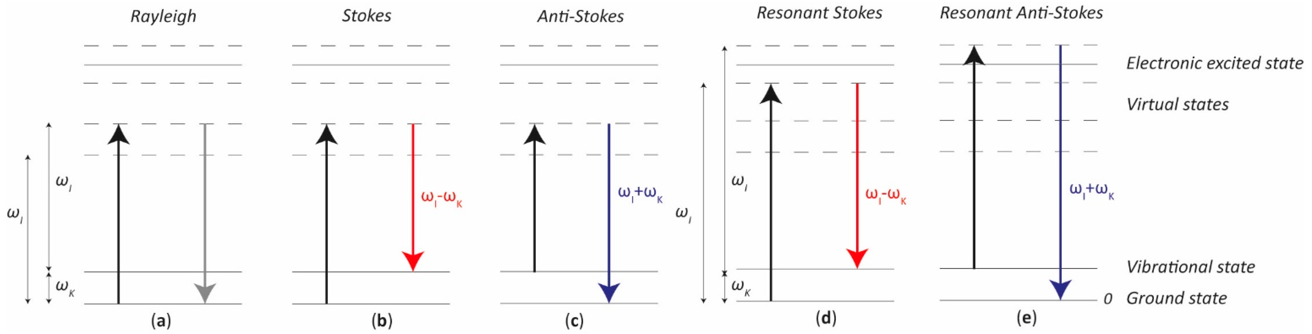
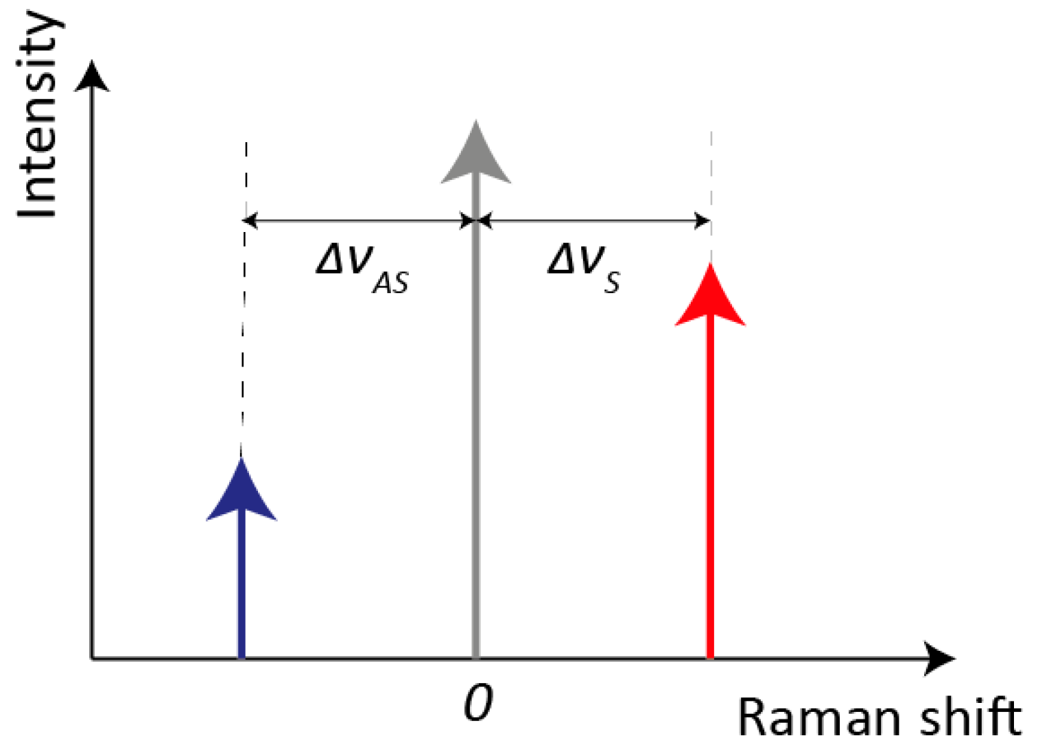
1.1. Raman Effect
1.2. Raman Spectra
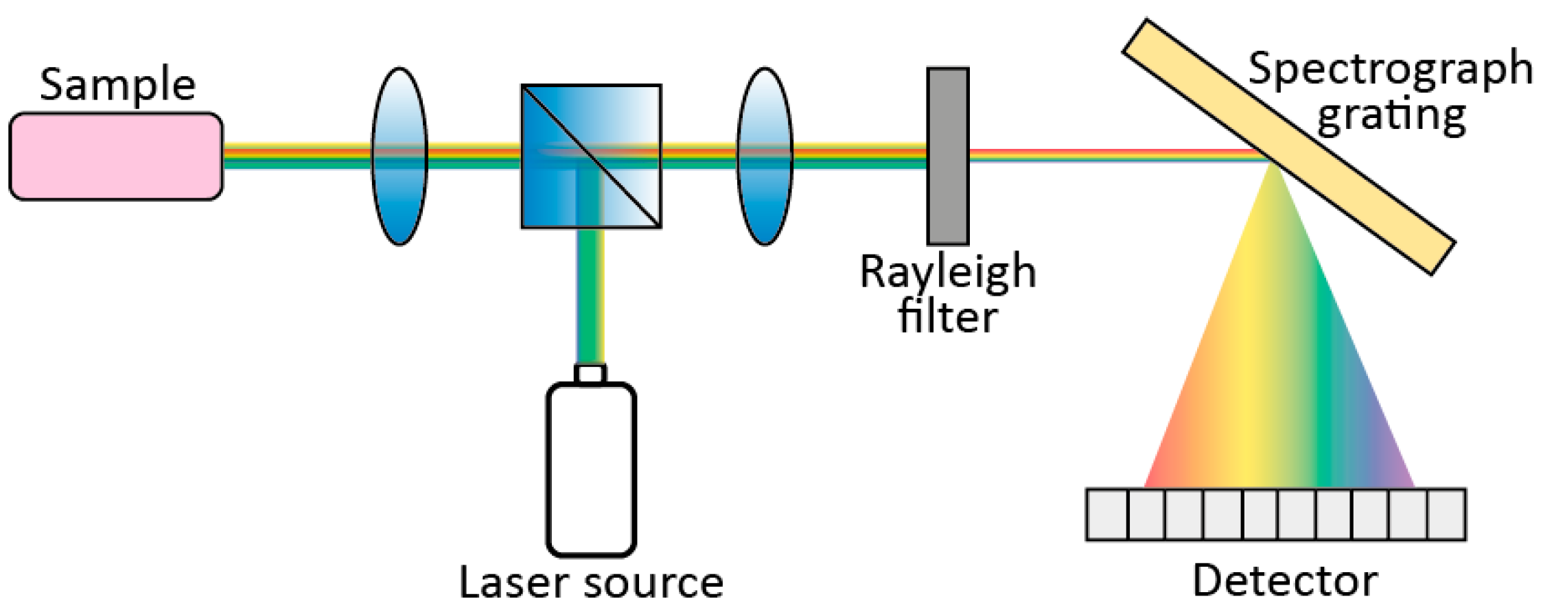
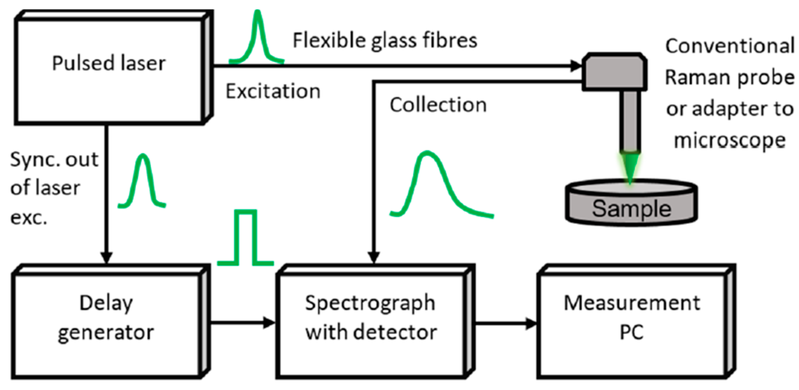
1.3. Raman Spectrometer System
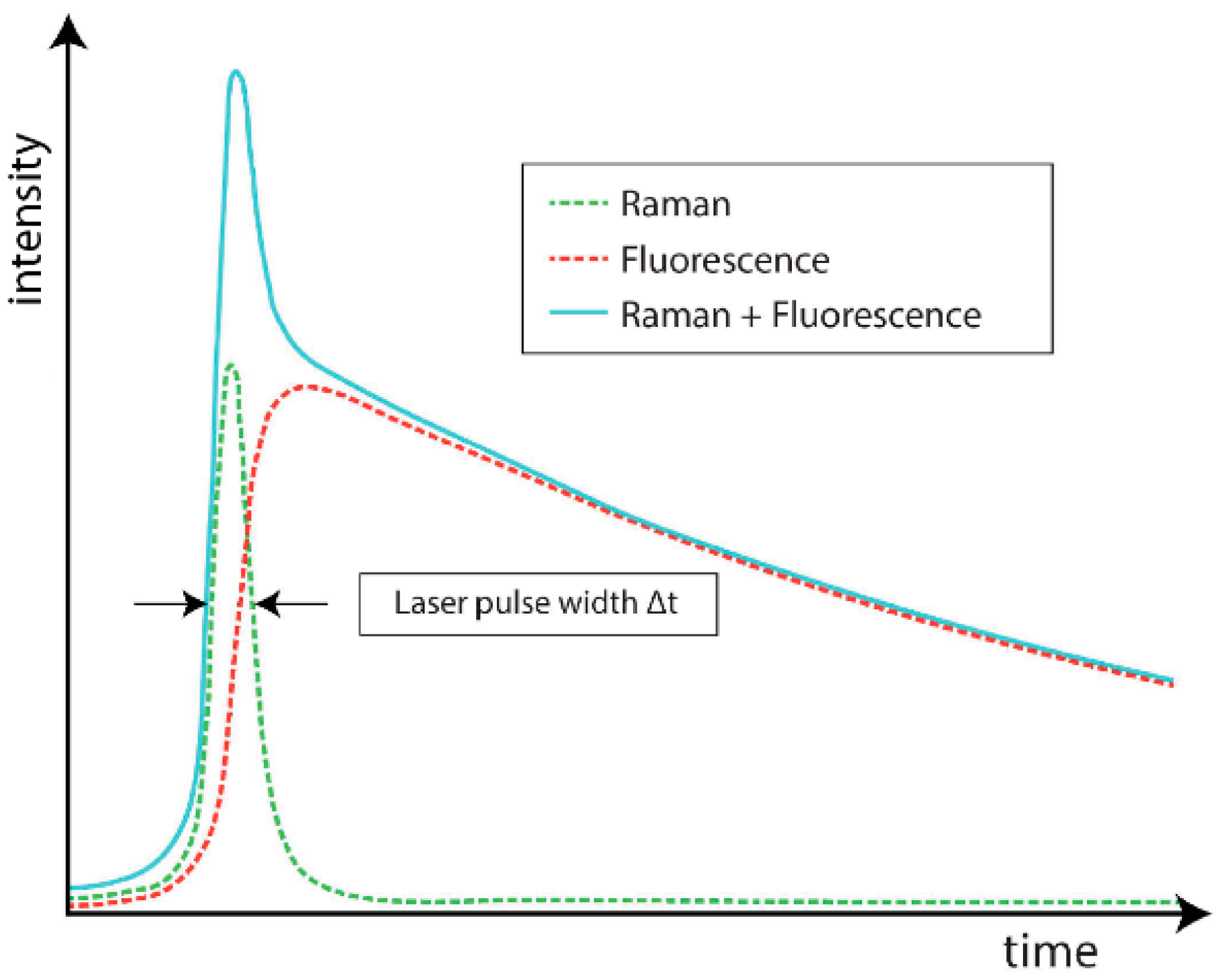
2. Detectors
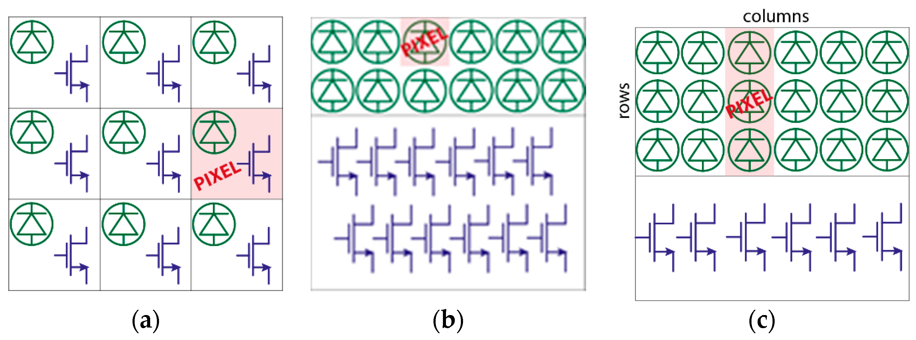
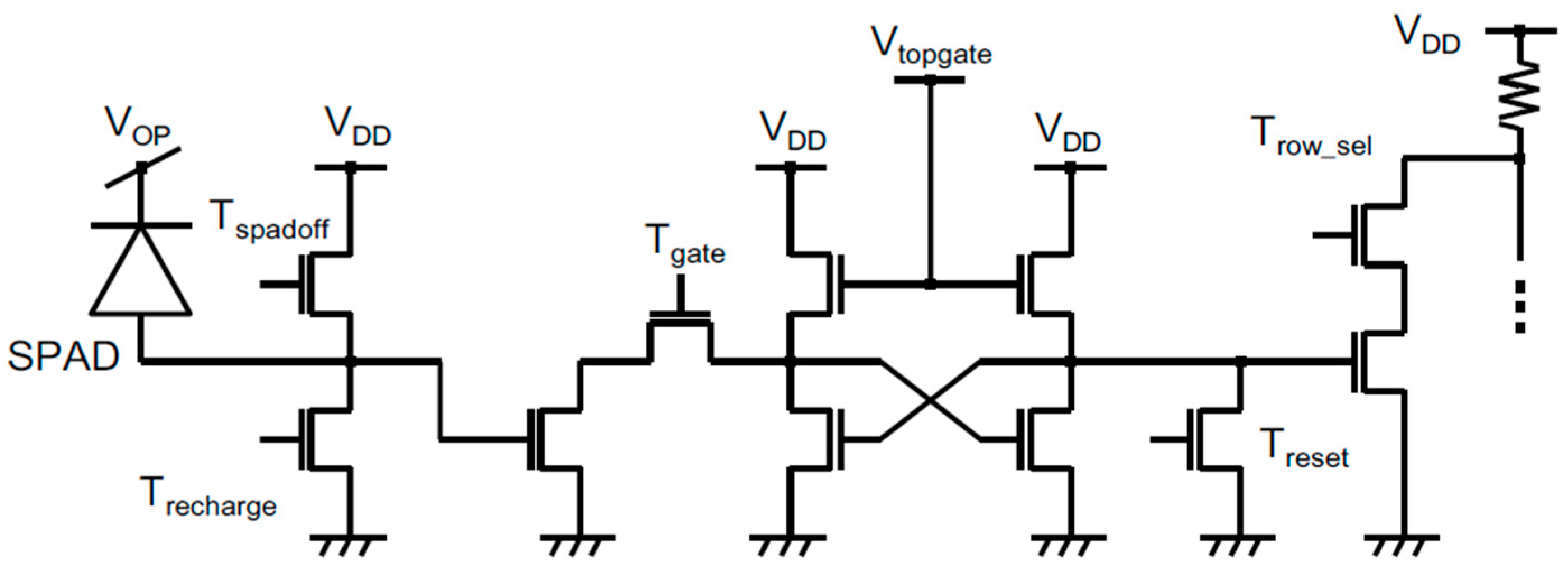
3. SPAD Array Requirements for TG Raman Spectroscopy
4. Review of SPAD Arrays for Raman Spectroscopy
4.1. 128 × 128 SPAD Camera
4.2. 1024 × 8 SPAD Line Sensor
4.3. 128 × 1 Multiphase Time-Gated SPAD Line Detector
4.4. 256 × 2 TRFS Line Sensor
4.5. 256 LinoSPAD Camera
4.6. 16 × 256 TDC-Based SPAD Line Detector
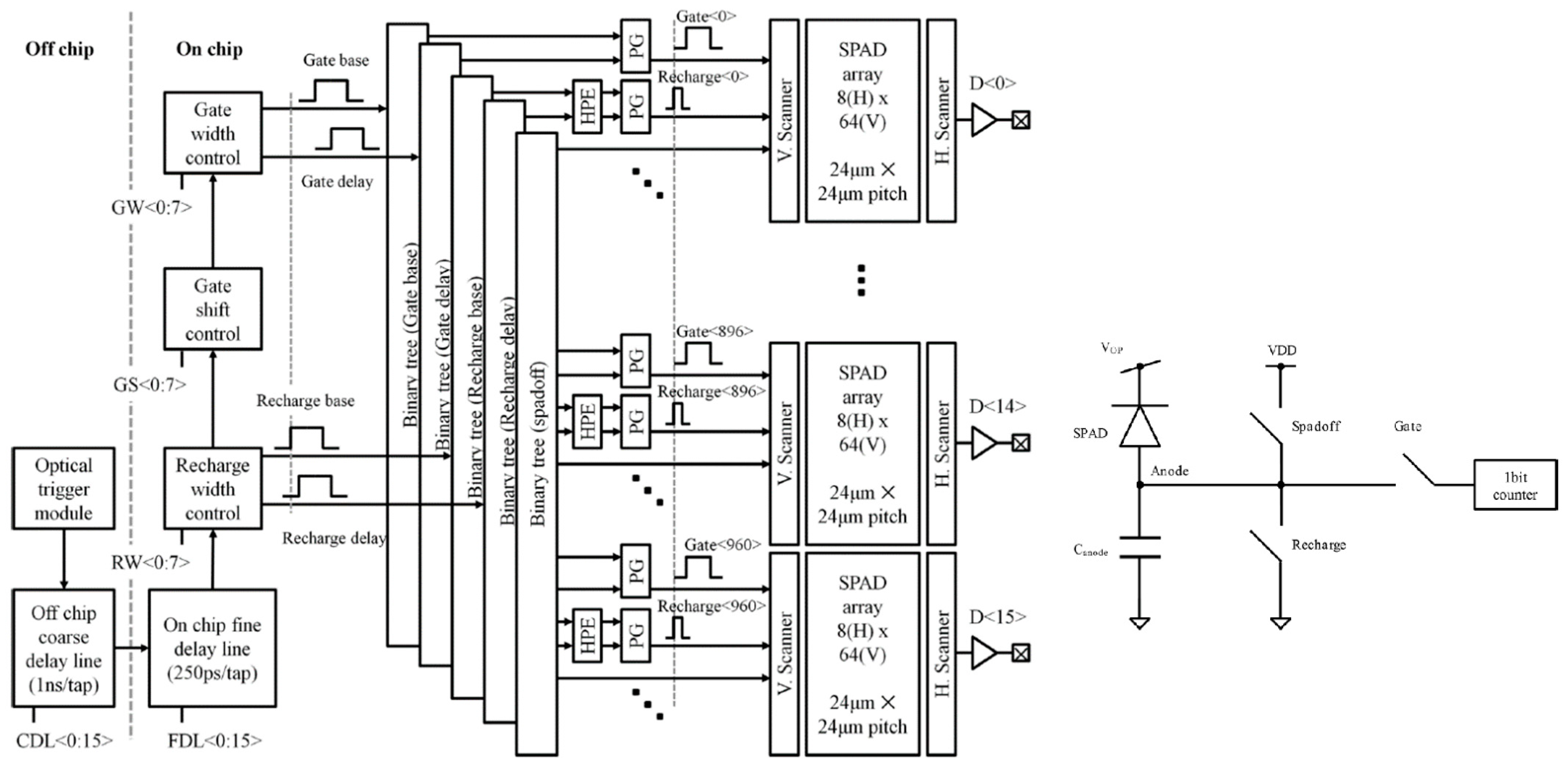
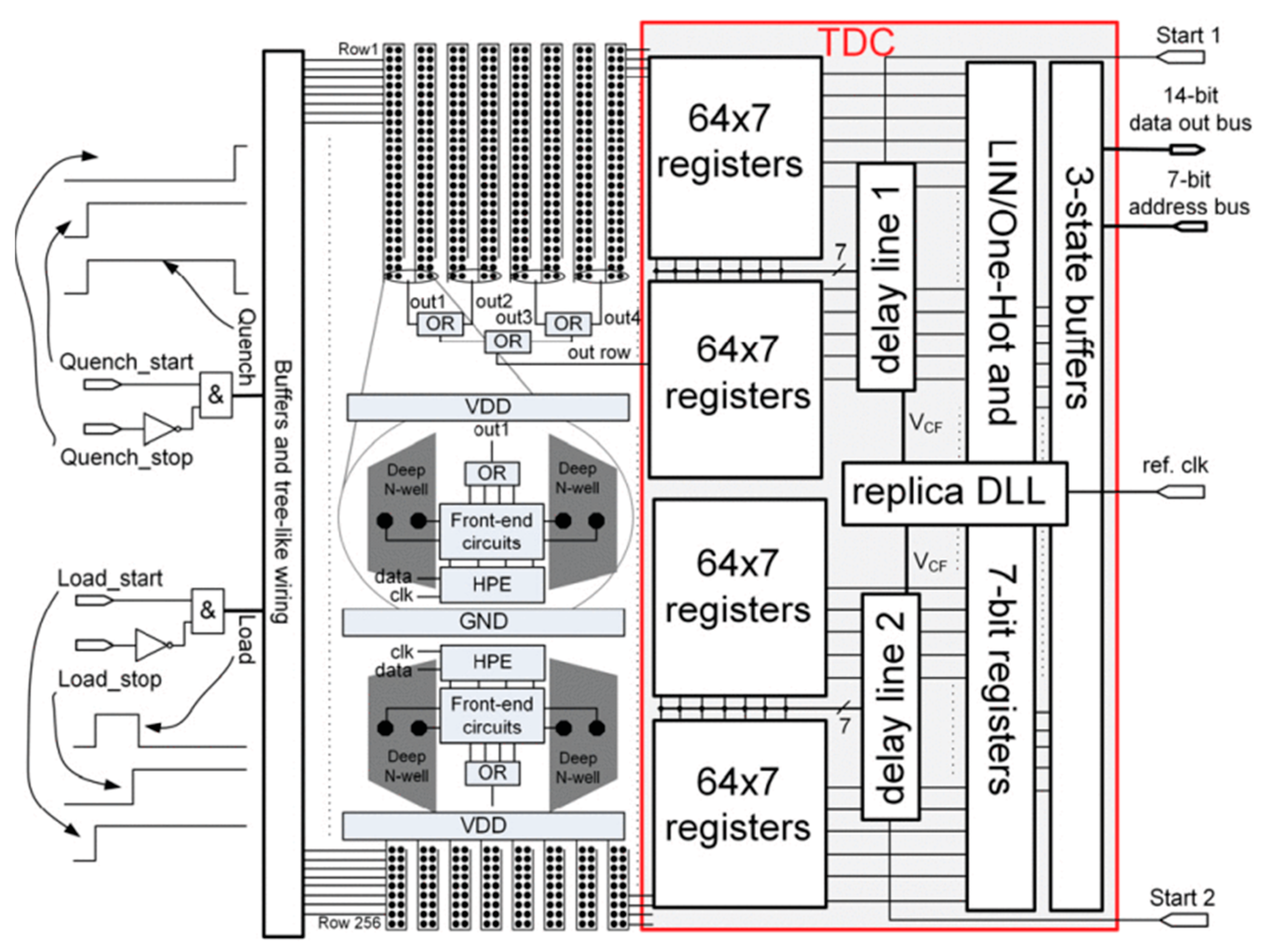
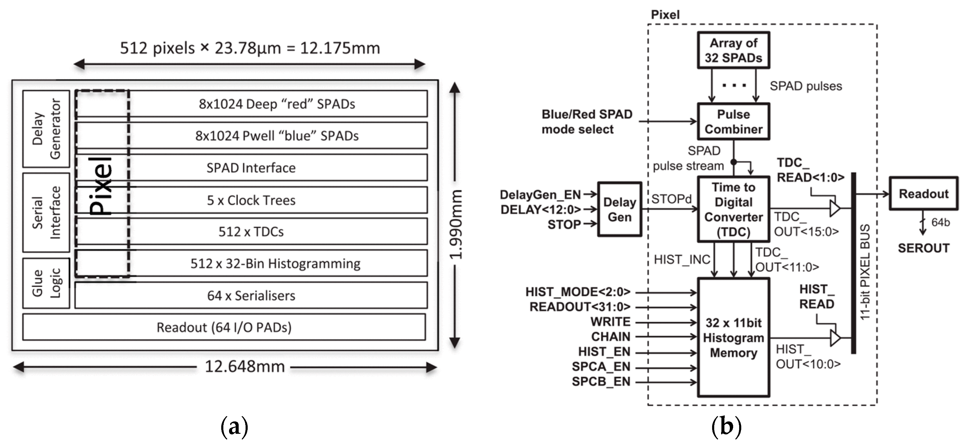
4.7. 512 × 16 SPAD Line Sensor with Per-Pixel Histogramming TDC
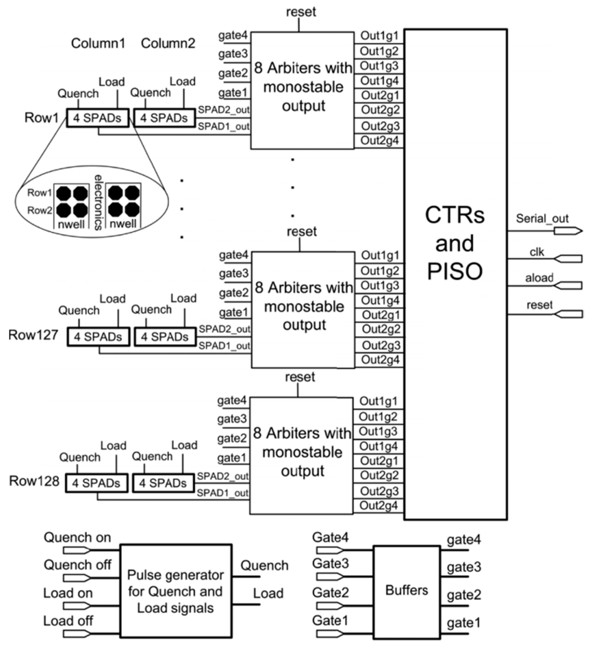
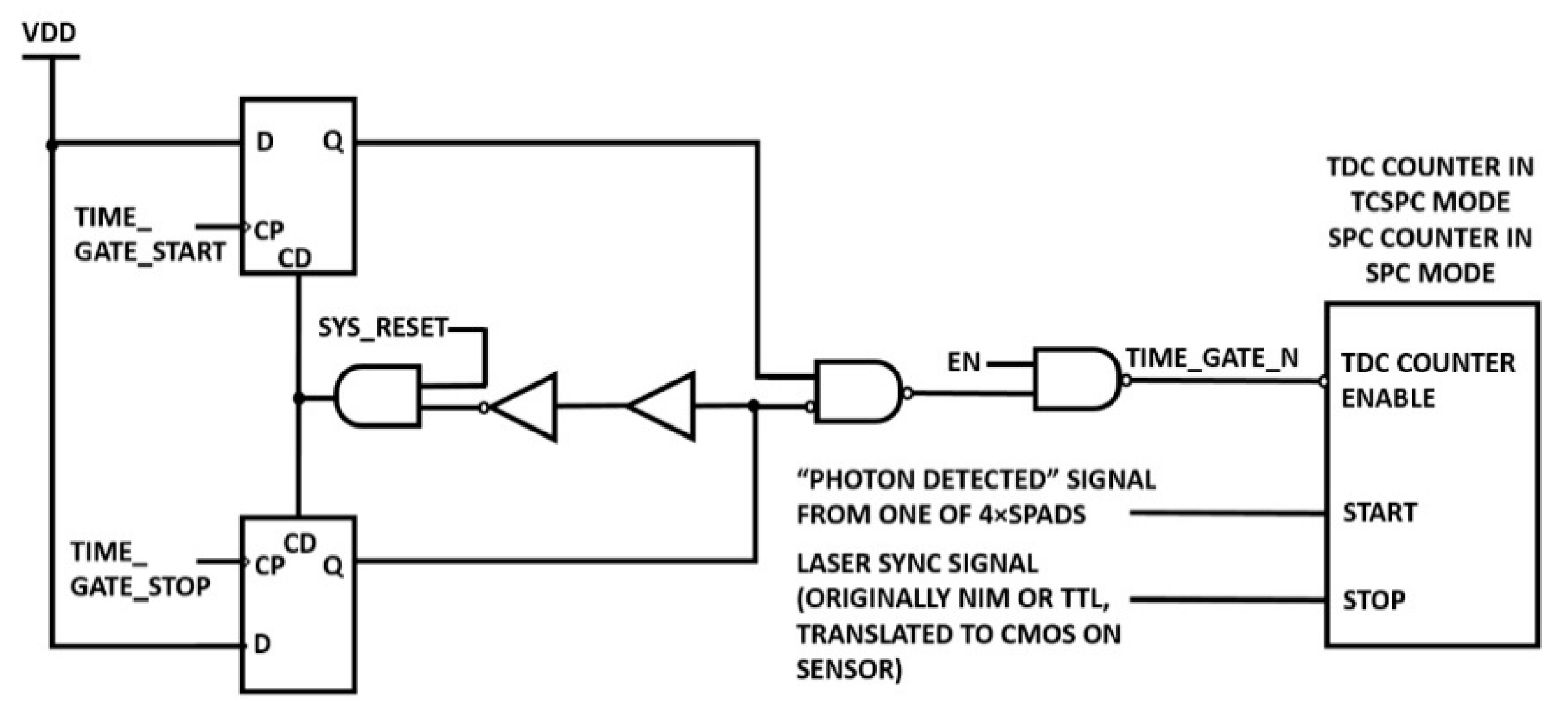
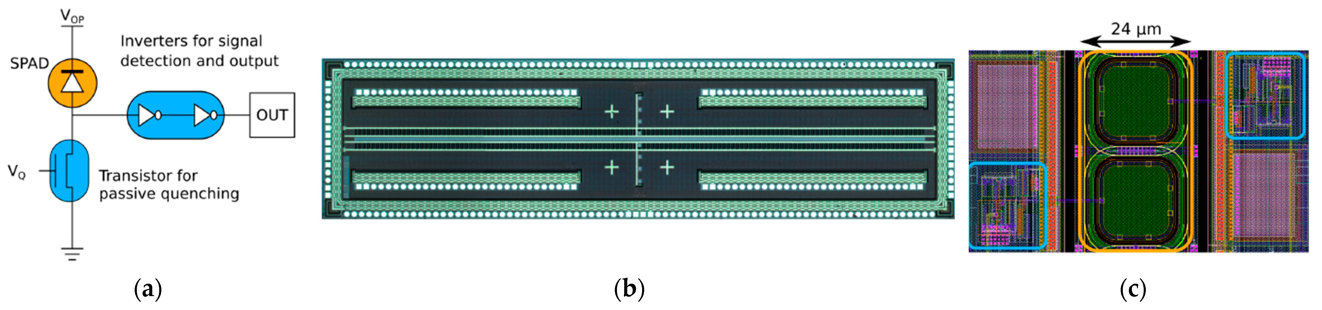
4.8. 128 × 1 Time-Gated SPAD Array
5. Discussion
6. Conclusions
Author Contributions
Funding
Conflicts of Interest
References
- Choo-Smith, L.-P.; Edwards, H.G.M.; Endtz, H.P.; Kros, J.M.; Heule, F.; Barr, H.; Robinson, J.S., Jr.; Bruining, H.A.; Puppels, G.J. Medical applications of Raman spectroscopy: From proof of principle to clinical implementation. Biopolymers 2002, 67, 1–9. [Google Scholar] [CrossRef]
- Kong, K.; Kendall, C.; Stone, N.; Notingher, I. Raman spectroscopy for medical diagnostics—From in-vitro biofluid assays to in-vivo cancer detection. Adv. Drug Deliv. Rev. 2015, 89, 121–134. [Google Scholar] [CrossRef] [Green Version]
- Ember, K.J.I.; Hoeve, M.A.; McAughtrie, S.L.; Bergholt, M.S.; Dwyer, B.J.; Stevens, M.M.; Faulds, K.; Forbes, S.J.; Campbell, C.J. Raman spectroscopy and regenerative medicine: A review. NPJ Regen. Med. 2017, 2, 12. [Google Scholar] [CrossRef] [PubMed]
- McMillan, P.F. Raman Spectroscopy in Mineralogy and Geochemistry. Annu. Rev. Earth Planet. Sci. 1989, 17, 255–279. [Google Scholar] [CrossRef]
- Nasdala, L.; Schmidt, C. Applications of Raman Spectroscopy in Mineralogy and Geochemistry. Elements 2020, 16, 99–104. [Google Scholar] [CrossRef]
- Vankeirsbilck, T.; Vercauteren, A.; Baeyens, W.; Van der Weken, G.; Verpoort, F.; Vergote, G.; Remon, J.P. Applications of Raman spectroscopy in pharmaceutical analysis. TrAC Trends Anal. Chem. 2002, 21, 869–877. [Google Scholar] [CrossRef]
- Fini, G. Applications of Raman spectroscopy to pharmacy. J. Raman Spectrosc. 2004, 35, 335–337. [Google Scholar] [CrossRef]
- Gala, U.; Chauhan, H. Principles and applications of Raman spectroscopy in pharmaceutical drug discovery and development. Expert Opin. Drug Discov. 2015, 10, 187–206. [Google Scholar] [CrossRef]
- Blacksberg, J.; Rossman, G.R.; Gleckler, A. Time-resolved Raman spectroscopy for in situ planetary mineralogy. Appl. Opt. 2010, 49, 4951–4962. [Google Scholar] [CrossRef] [Green Version]
- Angel, S.M.; Gomer, N.R.; Sharma, S.K.; McKay, C. Remote Raman Spectroscopy for Planetary Exploration: A Review. Appl. Spectrosc. 2012, 66, 137–150. [Google Scholar] [CrossRef] [Green Version]
- Veneranda, M.; Lopez-Reyes, G.; Manrique-Martinez, J.A.; Sanz-Arranz, A.; Medina, J.; Pérez, C.; Quintana, C.; Moral, A.; Rodríguez, J.A.; Zafra, J.; et al. Raman spectroscopy and planetary exploration: Testing the ExoMars/RLS system at the Tabernas Desert (Spain). Microchem. J. 2021, 165, 106149. [Google Scholar] [CrossRef]
- Raman, C.V.; Krishnan, K.S. A New Type of Secondary Radiation. Nature 1928, 121, 501–502. [Google Scholar] [CrossRef]
- Mandelstam, G.; Landsberg, L. Eine neue Erscheinung bei der Lichtzerstreuung in Krystallen. Naturwissenschaften 1928, 16, 557–558. [Google Scholar] [CrossRef]
- Gordon, R.G.; Klemperer, W.; Steinfeld, J.I. Vibrational and Rotational Relaxation. Annu. Rev. Phys. Chem. 1968, 19, 215–250. [Google Scholar] [CrossRef]
- Zhu, X.; Xu, T.; Lin, Q.; Duan, Y. Technical development of raman spectroscopy: From instrumental to advanced combined technologies. Appl. Spectrosc. Rev. 2014, 49, 64–82. [Google Scholar] [CrossRef]
- Blacksberg, J.; Alerstam, E.; Maruyama, Y.; Cochrane, C.J.; Rossman, G.R. Miniaturized time-resolved Raman spectrometer for planetary science based on a fast single photon avalanche diode detector array. Appl. Opt. 2016, 55, 739. [Google Scholar] [CrossRef] [Green Version]
- Kauffmann, T.H.; Kokanyan, N.; Fontana, M.D. Use of Stokes and anti-Stokes Raman scattering for new applications. J. Raman Spectrosc. 2019, 50, 418–424. [Google Scholar] [CrossRef]
- Lakowicz, J. (Ed.) Principles of Fluorescence Spectroscopy, 3rd ed.; Springer: Boston, MA, USA, 1983. [Google Scholar]
- Grabarnik, S.; Emadi, A.; Sokolova, E.; Vdovin, G.; Wolffenbuttel, R.F. Optimal implementation of a microspectrometer based on a single flat diffraction grating. Appl. Opt. 2008, 47, 2082–2090. [Google Scholar] [CrossRef] [Green Version]
- Long, D.A. The Raman Effect: A Unified Treatment of the Theory of Raman Scattering by Molecules; John Wiley & Sons, Ltd.: Chichester, West Sussex, UK, 2002. [Google Scholar]
- Villa, F.; Bronzi, D.; Zou, Y.; Scarcella, C.; Boso, G.; Tisa, S.; Tosi, A.; Zappa, F.; Durini, D.; Weyers, S.; et al. CMOS SPADs with up to 500 μm diameter and 55% detection efficiency at 420 nm. J. Mod. Opt. 2014, 61, 102–115. [Google Scholar] [CrossRef]
- Abbey, W.J.; Bhartia, R.; Beegle, L.W.; De Flores, L.; Paez, V.; Sijapati, K.; Sijapati, S.; Williford, K.; Tuite, M.; Hug, W.; et al. Deep UV Raman spectroscopy for planetary exploration: The search for in situ organics. Icarus 2017, 290, 201–214. [Google Scholar] [CrossRef]
- Macdonald, A.M.; Wyeth, P. On the use of photobleaching to reduce fluorescence background in Raman spectroscopy to improve the reliability of pigment identification on painted textiles. J. Raman Spectrosc. 2006, 37, 830–835. [Google Scholar] [CrossRef] [Green Version]
- Wei, D.; Chen, S.; Liu, Q. Review of Fluorescence Suppression Techniques in Raman Spectroscopy. Appl. Spectrosc. Rev. 2015, 50, 387–406. [Google Scholar] [CrossRef]
- Hooijschuur, J.-H.; Iping Petterson, I.E.; Davies, G.R.; Gooijer, C.; Ariese, F. Time resolved Raman spectroscopy for depth analysis of multi-layered mineral samples. J. Raman Spectrosc. 2013, 44, 1540–1547. [Google Scholar] [CrossRef]
- Rojalin, T.; Kurki, L.; Laaksonen, T.; Viitala, T.; Kostamovaara, J.; Gordon, K.C.; Galvis, L.; Wachsmann-Hogiu, S.; Strachan, C.J.; Yliperttula, M. Fluorescence-suppressed time-resolved Raman spectroscopy of pharmaceuticals using complementary metal-oxide semiconductor (CMOS) single-photon avalanche diode (SPAD) detector. Anal. Bioanal. Chem. 2016, 408, 761–774. [Google Scholar] [CrossRef]
- Oracz, J.; Westphal, V.; Radzewicz, C.; Sahl, S.J.; Hell, S.W. Photobleaching in STED nanoscopy and its dependence on the photon flux applied for reversible silencing of the fluorophore. Sci. Rep. 2017, 7, 11354. [Google Scholar] [CrossRef] [Green Version]
- Angel, S.M.; DeArmond, M.K.; Hanck, K.W.; Wertz, D.W. Computer-controlled instrument for the recovery of a resonance Raman spectrum in the presence of strong luminescence. Anal. Chem. 1984, 56, 3000–3001. [Google Scholar] [CrossRef]
- Zhao, J.; Lui, H.; McLean, D.I.; Zeng, H. Automated Autofluorescence Background Subtraction Algorithm for Biomedical Raman Spectroscopy. Appl. Spectrosc. 2007, 61, 1225–1232. [Google Scholar] [CrossRef] [PubMed]
- Zhang, Z.-M.; Chen, S.; Liang, Y.-Z.; Liu, Z.-X.; Zhang, Q.-M.; Ding, L.-X.; Ye, F.; Zhou, H. An intelligent background-correction algorithm for highly fluorescent samples in Raman spectroscopy. J. Raman Spectrosc. 2010, 41, 659–669. [Google Scholar] [CrossRef]
- Cadusch, P.J.; Hlaing, M.M.; Wade, S.A.; McArthur, S.L.; Stoddart, P.R. Improved methods for fluorescence background subtraction from Raman spectra. J. Raman Spectrosc. 2013, 44, 1587–1595. [Google Scholar] [CrossRef] [Green Version]
- Kögler, M.; Heilala, B. Time-gated Raman spectroscopy—A review. Meas. Sci. Technol. 2020, 32, 012002. [Google Scholar] [CrossRef]
- Rank, D.H.; Pfister, R.J.; Coleman, P.D. Photoelectric Detection and Intensity Measurement in Raman Spectra. J. Opt. Soc. Am. 1942, 32, 390–396. [Google Scholar] [CrossRef]
- Matsuoka, K.; Hirose, S.; Iijima, T.; Inami, K.; Kato, Y.; Kobayashi, K.; Maeda, Y.; Omori, R.; Suzuki, K. Extension of the MCP-PMT lifetime. Nucl. Instrum. Methods Phys. Res. Sect. A Accel. Spectrometers Detect. Assoc. Equip. 2017, 876, 93–95. [Google Scholar] [CrossRef]
- Murray, C.A.; Dierker, S.B. Use of an unintensified charge-coupled device detector for low-light-level Raman spectroscopy. J. Opt. Soc. Am. A 1986, 3, 2151–2159. [Google Scholar] [CrossRef]
- Burke, B.; Jorden, P.; Vu, P. CCD Technology. Exp. Astron. 2005, 19, 69–102. [Google Scholar] [CrossRef]
- Baraga, J.J.; Feld, M.S.; Rava, R.P. Rapid Near-Infrared Raman Spectroscopy of Human Tissue with a Spectrograph and CCD Detector. Appl. Spectrosc. 1992, 46, 187–190. [Google Scholar] [CrossRef]
- Matousek, P.; Towrie, M.; Ma, C.; Kwok, W.M.; Phillips, D.; Toner, W.T.; Parker, A.W. Fluorescence suppression in resonance Raman spectroscopy using a high-performance picosecond Kerr gate. J. Raman Spectrosc. 2001, 32, 983–988. [Google Scholar] [CrossRef]
- Tahara, T.; Hamaguchi, H.-O. Picosecond Raman Spectroscopy Using a Streak Camera. Appl. Spectrosc. 1993, 47, 391–398. [Google Scholar] [CrossRef]
- Cester, L.; Lyons, A.; Braidotti, M.C.; Faccio, D. Time-of-Flight Imaging at 10 ps Resolution with an ICCD Camera. Sensors 2019, 19, 180. [Google Scholar] [CrossRef] [Green Version]
- Martyshkin, D.V.; Ahuja, R.C.; Kudriavtsev, A.; Mirov, S.B. Effective suppression of fluorescence light in Raman measurements using ultrafast time gated charge coupled device camera. Rev. Sci. Instrum. 2004, 75, 630–635. [Google Scholar] [CrossRef] [Green Version]
- Chiuri, A.; Angelini, F. Fast gating for Raman spectroscopy. Sensors 2021, 21. [Google Scholar] [CrossRef] [PubMed]
- Gulinatti, A.; Ceccarelli, F.; Ghioni, M.; Rech, I. Custom silicon technology for SPAD-arrays with red-enhanced sensitivity and low timing jitter. Opt. Express 2021, 29, 4559–4581. [Google Scholar] [CrossRef]
- Ceccarelli, F.; Acconcia, G.; Gulinatti, A.; Ghioni, M.; Rech, I.; Osellame, R. Recent Advances and Future Perspectives of Single-Photon Avalanche Diodes for Quantum Photonics Applications. Adv. Quantum Technol. 2021, 4, 2000102. [Google Scholar] [CrossRef]
- Dautet, H.; Deschamps, P.; Dion, B.; MacGregor, A.D.; MacSween, D.; McIntyre, R.J.; Trottier, C.; Webb, P.P. Photon counting techniques with silicon avalanche photodiodes. Appl. Opt. 1993, 32, 3894–3900. [Google Scholar] [CrossRef] [Green Version]
- Acerbi, F.; Anti, M.; Tosi, A.; Zappa, F. Design Criteria for InGaAs/InP Single-Photon Avalanche Diode. IEEE Photonics J. 2013, 5, 6800209. [Google Scholar] [CrossRef] [Green Version]
- Tosi, A.; Ruggeri, A.; Villa, F.; Sanzaro, M.; Buttafava, M.; Calandri, N.; Zappa, F. Short-gate techniques for high-speed photon counting with InGaAs/InP SPADs. In Proceedings of the 2016 Conference on Lasers and Electro-Optics (CLEO), San Jose, CA, USA, 5–10 June 2016; pp. 1–2. [Google Scholar]
- Aminian, M.; Sammak, A.; Qi, L.; Nanver, L.K.; Charbon, E. A Ge-on-Si single-photon avalanche diode operating in Geiger mode at infrared wavelengths. In Proceedings of the SPIE, Baltimore, MD, USA, 22 May 2012; Volume 8375. [Google Scholar]
- Dumas, D.C.S.; Kirdoda, J.; Vines, P.; Kuzmenko, K.; Millar, R.W.; Buller, G.S.; Paul, D.J. Ge-On-Si High Efficiency Spads at 1310 nm. In Proceedings of the 2019 Conference on Lasers and Electro-Optics Europe & European Quantum Electronics Conference (CLEO/Europe-EQEC), Munich, Germany, 23–27 June 2019; p. 1. [Google Scholar]
- Nissinen, I.; Nissinen, J.; Länsman, A.K.; Hallman, L.; Kilpelä, A.; Kostamovaara, J.; Kögler, M.; Aikio, M.; Tenhunen, J. A sub-ns time-gated CMOS single photon avalanche diode detector for Raman spectroscopy. Eur. Solid-State Device Res. Conf. 2011, 375–378. [Google Scholar] [CrossRef]
- Kostamovaara, J.; Tenhunen, J.; Kögler, M.; Nissinen, I.; Nissinen, J.; Keränen, P. Fluorescence suppression in Raman spectroscopy using a time-gated CMOS SPAD. Opt. Express 2013, 21, 31632–31645. [Google Scholar] [CrossRef]
- Bruschini, C.; Homulle, H.; Antolovic, I.M.; Burri, S.; Charbon, E. Single-photon avalanche diode imagers in biophotonics: Review and outlook. Light Sci. Appl. 2019, 8. [Google Scholar] [CrossRef] [PubMed]
- Lee, M.J.; Charbon, E. Progress in single-photon avalanche diode image sensors in standard CMOS: From two-dimensional monolithic to three-dimensional-stacked technology. Jpn. J. Appl. Phys. 2018, 57, 1002A3. [Google Scholar] [CrossRef]
- Arnaud, T.; Leverd, F.; Favennec, L.; Perrot, C.; Pinzelli, L.; Gatefait, M.; Cherault, N.; Jeanjean, D.; Carrere, J.-P.; Hirigoyen, F.; et al. Pixel-to-Pixel isolation by Deep Trench technology: Application to CMOS Image Sensor. In Proceedings of the IISW 2011, Hokkaido, Japan, 8–11 June 2011. [Google Scholar]
- Ghioni, M.; Gulinatti, A.; Rech, I.; Zappa, F.; Cova, S. Progress in Silicon Single-Photon Avalanche Diodes. IEEE J. Sel. Top. Quantum Electron. 2007, 13, 852–862. [Google Scholar] [CrossRef]
- Nissinen, I.; Lansman, A.K.; Nissinen, J.; Holma, J.; Kostamovaara, J. 2 × (4×)128 time-gated CMOS single photon avalanche diode line detector with 100 ps resolution for Raman spectroscopy. Eur. Solid-State Circuits Conf. 2013, 291–294. [Google Scholar] [CrossRef]
- Nissinen, I.; Nissinen, J.; Keränen, P.; Kostamovaara, J. On the effects of the time gate position and width on the signal-to-noise ratio for detection of Raman spectrum in a time-gated CMOS single-photon avalanche diode based sensor. Sens. Actuators B Chem. 2017, 241, 1145–1152. [Google Scholar] [CrossRef]
- Bronzi, D.; Tisa, S.; Villa, F.; Bellisai, S.; Tosi, A.; Zappa, F. Fast Sensing and Quenching of CMOS SPADs for Minimal Afterpulsing Effects. IEEE Photonics Technol. Lett. 2013, 25, 776–779. [Google Scholar] [CrossRef]
- Kekkonen, J.; Talala, T.; Nissinen, J.; Nissinen, I. On the Spectral Quality of Time-Resolved CMOS SPAD-Based Raman Spectroscopy with High Fluorescence Backgrounds. IEEE Sens. J. 2020, 20, 4635–4645. [Google Scholar] [CrossRef] [Green Version]
- Gulinatti, A.; Rech, I.; Assanelli, M.; Ghioni, M.; Cova, S. A physically based model for evaluating the photon detection efficiency and the temporal response of SPAD detectors. J. Mod. Opt. 2011, 58, 210–224. [Google Scholar] [CrossRef] [Green Version]
- Sanzaro, M.; Gattari, P.; Villa, F.; Tosi, A.; Croce, G.; Zappa, F. Single-Photon Avalanche Diodes in a 0.16 μm BCD Technology With Sharp Timing Response and Red-Enhanced Sensitivity. IEEE J. Sel. Top. Quantum Electron. 2018, 24, 1–9. [Google Scholar] [CrossRef] [Green Version]
- Haitz, R.H. Mechanisms Contributing to the Noise Pulse Rate of Avalanche Diodes. J. Appl. Phys. 1965, 36, 3123–3131. [Google Scholar] [CrossRef]
- Maruyama, Y.; Blacksberg, J.; Charbon, E. A time-resolved 128 × 128 SPAD camera for laser Raman spectroscopy. Next-Gener. Spectrosc. Technol. V 2012, 8374, 83740N. [Google Scholar] [CrossRef]
- BECKER, W. Fluorescence lifetime imaging—Techniques and applications. J. Microsc. 2012, 247, 119–136. [Google Scholar] [CrossRef] [PubMed]
- Maruyama, Y.; Blacksberg, J.; Charbon, E. A 1024 × 8 700ps Time-Gated SPAD Line Sensor for Laser Raman Spectroscopy and LIBS in Space and Rover-Based Planetary Exploration. In Proceedings of the ISSCC, San Francisco, CA, USA, 17–21 February 2013; Volume 3, pp. 106–108. [Google Scholar]
- Maruyama, Y.; Blacksberg, J.; Charbon, E. A 1024 × 8, 700-ps time-gated spad line sensor for planetary surface exploration with laser raman spectroscopy and libs. IEEE J. Solid-State Circuits 2014, 49, 179–189. [Google Scholar] [CrossRef]
- Cremers, D.A.; Multari, R.A.; Knight, A.K. Laser-Induced Breakdown Spectroscopy; Cambridge University Press: Cambridge, UK, 2006. [Google Scholar]
- Kufcsák, A.; Erdogan, A.; Walker, R.; Ehrlich, K.; Tanner, M.; Megia-Fernandez, A.; Scholefield, E.; Emanuel, P.; Dhaliwal, K.; Bradley, M.; et al. Time-resolved spectroscopy at 19,000 lines per second using a CMOS SPAD line array enables advanced biophotonics applications. Opt. Express 2017, 25, 11103. [Google Scholar] [CrossRef] [PubMed] [Green Version]
- Krstajić, N.; Levitt, J.; Poland, S.; Ameer-Beg, S.; Henderson, R. 256 × 2 SPAD line sensor for time resolved fluorescence spectroscopy. Opt. Express 2015, 23, 5653. [Google Scholar] [CrossRef] [Green Version]
- Yankelevich, D.R.; Ma, D.; Liu, J.; Sun, Y.; Sun, Y.; Bec, J.; Elson, D.S.; Marcu, L. Design and evaluation of a device for fast multispectral time-resolved fluorescence spectroscopy and imaging. Rev. Sci. Instrum. 2014, 85, 34303. [Google Scholar] [CrossRef] [Green Version]
- Hirvonen, L.M.; Suhling, K. Wide-field TCSPC: Methods and applications. Meas. Sci. Technol. 2016, 28, 12003. [Google Scholar] [CrossRef]
- Burri, S.; Bruschini, C.; Charbon, E. LinoSPAD: A Compact Linear SPAD Camera System with 64 FPGA-Based TDC Modules for Versatile 50 ps Resolution Time-Resolved Imaging. Instruments 2017, 1, 6. [Google Scholar] [CrossRef] [Green Version]
- Nissinen, I.; Nissinen, J.; Keranen, P.; Stoppa, D.; Kostamovaara, J. A 16 × 256 SPAD Line Detector with a 50-ps, 3-bit, 256-Channel Time-to-Digital Converter for Raman Spectroscopy. IEEE Sens. J. 2018, 18, 3789–3798. [Google Scholar] [CrossRef] [Green Version]
- Nissinen, I.; Nissinen, J.; Holma, J.; Kostamovaara, J. A 4 × 128 SPAD array with a 78-ps 512-channel TDC for time-gated pulsed Raman spectroscopy. Analog. Integr. Circuits Signal Process. 2015, 84, 353–362. [Google Scholar] [CrossRef]
- Erdogan, A.T.; Walker, R.; Finlayson, N.; Krstajic, N.; Williams, G.; Girkin, J.; Henderson, R. A CMOS SPAD Line Sensor with Per-Pixel Histogramming TDC for Time-Resolved Multispectral Imaging. IEEE J. Solid-State Circuits 2019, 54, 1705–1719. [Google Scholar] [CrossRef] [Green Version]
- Usai, A.; Finlayson, N.; Gregory, C.D.; Campbell, C.; Henderson, R.K. Separating fluorescence from Raman spectra using a CMOS SPAD TCSPC line sensor for biomedical applications. In Proceedings of the Optical Biopsy XVII: Toward Real-Time Spectroscopic Imaging and Diagnosis, San Francisco, CA, USA, 4 March 2019. [Google Scholar] [CrossRef]
- Conca, E.; Cusini, I.; Severini, F.; Lussana, R.; Zappa, F.; Villa, F. Gated SPAD Arrays for Single-Photon Time-Resolved Imaging and Spectroscopy. IEEE Photonics J. 2019, 11. [Google Scholar] [CrossRef]
- Cusini, I.; Pasquinelli, K.; Conca, E.; Villa, F. Time-gated 128 × 1 and 8 × 8 SPAD cameras for 2D photon-counting and 3D time-of-flight maps. In Proceedings of the Quantum Optics and Photon Counting 2021, online, 18 April 2021; pp. 1–10. [Google Scholar] [CrossRef]
- Bronzi, D.; Zou, Y.; Villa, F.; Tisa, S.; Tosi, A.; Zappa, F. Automotive Three-Dimensional Vision Through a Single-Photon Counting SPAD Camera. IEEE Trans. Intell. Transp. Syst. 2016, 17, 782–795. [Google Scholar] [CrossRef] [Green Version]
- Bouchard, J.; Samson, A.; Lemaire, W.; Paulin, C.; Pratte, J.; Bérubé-Lauzière, Y.; Fontaine, R. A Low-Cost Time-Correlated Single Photon Counting System for Multiview Time-Domain Diffuse Optical Tomography. IEEE Trans. Instrum. Meas. 2017, 66, 2505–2515. [Google Scholar] [CrossRef]
- Unternährer, M.; Bessire, B.; Gasparini, L.; Stoppa, D.; Stefanov, A. Coincidence detection of spatially correlated photon pairs with a novel type of monolithic time-resolving detector array. In Proceedings of the 2017 Conference on Lasers and Electro-Optics Europe & European Quantum Electronics Conference (CLEO/Europe-EQEC), Munich, Germany, 25–29 June 2017; p. 1. [Google Scholar]
- Markovic, B.; Tisa, S.; Villa, F.A.; Tosi, A.; Zappa, F. A High-Linearity, 17 ps Precision Time-to-Digital Converter Based on a Single-Stage Vernier Delay Loop Fine Interpolation. IEEE Trans. Circuits Syst. I Regul. Pap. 2013, 60, 557–569. [Google Scholar] [CrossRef]
- Intermite, G.; McCarthy, A.; Warburton, R.E.; Ren, X.; Villa, F.; Lussana, R.; Waddie, A.J.; Taghizadeh, M.R.; Tosi, A.; Zappa, F.; et al. Fill-factor improvement of Si CMOS single-photon avalanche diode detector arrays by integration of diffractive microlens arrays. Opt. Express 2015, 23, 33777–33791. [Google Scholar] [CrossRef] [Green Version]
- Al Abbas, T.; Dutton, N.A.W.; Almer, O.; Pellegrini, S.; Henrion, Y.; Henderson, R.K. Backside illuminated SPAD image sensor with 7.83 μm pitch in 3D-stacked CMOS technology. In Proceedings of the 2016 IEEE International Electron Devices Meeting (IEDM), San Francisco, CA, USA, 3–7 December 2016; pp. 8.1.1–8.1.4. [Google Scholar]
- Pellegrini, S.; Rae, B.; Pingault, A.; Golanski, D.; Jouan, S.; Lapeyre, C.; Mamdy, B. Industrialised SPAD in 40 nm technology. In Proceedings of the 2017 IEEE International Electron Devices Meeting (IEDM), San Francisco, CA, USA, 2–6 December 2017; pp. 16.5.1–16.5.4. [Google Scholar] [CrossRef]
- Ximenes, A.R.; Padmanabhan, P.; Lee, M.; Yamashita, Y.; Yaung, D.; Charbon, E. A Modular, Direct Time-of-Flight Depth Sensor in 45/65-nm 3-D-Stacked CMOS Technology. IEEE J. Solid-State Circuits 2019, 54, 3203–3214. [Google Scholar] [CrossRef]
- Padmanabhan, P.; Zhang, C.; Cazzaniga, M.; Efe, B.; Ximenes, A.R.; Lee, M.-J.; Charbon, E. 7.4 A 256 × 128 3D-Stacked (45 nm) SPAD FLASH LiDAR with 7-Level Coincidence Detection and Progressive Gating for 100m Range and 10 klux Background Light. In Proceedings of the 2021 IEEE International Solid- State Circuits Conference (ISSCC), San Francisco, CA, USA, 13–22 February 2021; Volume 64, pp. 111–113. [Google Scholar] [CrossRef]

| SPC | TCSPC | |
| Detection method | 128 × 128 SPAD camera [63] | 256 × 2 TRFS line sensor [68] |
| 1024 × 8 SPAD line sensor [66] | 16 × 256 TDC-based SPAD line detector [73] | |
| 128 × 1 Multiphase time-gated SPAD line detector [56] | 512 × 16 SPAD line sensor with per-pixel histogramming TDC [75] | |
| 256 × 2 TRFS line sensor [68] | 128 × 1 time-gated SPAD array [78] | |
| 256 LinoSPAD camera [72] (off-chip) | ||
| Gating mode | “Hard-gating” | “Soft-gating” |
| 128 × 128 SPAD camera [63] | 256 × 2 TRFS line sensor [68] | |
| 1024 × 8 SPAD line sensor [66] | ||
| 128 × 1 Multiphase time-gated SPAD line detector [56] | ||
| 16 × 256 TDC-based SPAD line detector [73] | ||
| 512 × 16 SPAD line sensor with per-pixel histogramming TDC [75] | ||
| 128 × 1 time-gated SPAD array [78] | ||
| Delay line implementation | Off-chip | On-chip |
| 128 × 128 SPAD camera [63] | 1024 × 8 SPAD line sensor [66] (off-chip coarse and on-chip fine delay line) | |
| 128 × 1 Multiphase time-gated SPAD line detector [56] | 512 × 16 SPAD line sensor with per-pixel histogramming TDC [75] | |
| 256 × 2 TRFS line sensor [68] | ||
| 16 × 256 TDC-based SPAD line detector [73] | ||
| Readout mode | Rolling shutter | Global shutter |
| 128 × 128 SPAD camera [63] | 128 × 1 Multiphase time-gated SPAD line detector [56] | |
| 16 × 256 TDC-based SPAD line detector [73] | ||
| the 512 × 16 SPAD line sensor with per-pixel histogramming TDC [75] | ||
| 128 × 1 time-gated SPAD array [78] | ||
| 256 × 2 TRFS line Sensor [68] |
Publisher’s Note: MDPI stays neutral with regard to jurisdictional claims in published maps and institutional affiliations. |
© 2021 by the authors. Licensee MDPI, Basel, Switzerland. This article is an open access article distributed under the terms and conditions of the Creative Commons Attribution (CC BY) license (https://creativecommons.org/licenses/by/4.0/).
Share and Cite
Madonini, F.; Villa, F. Single Photon Avalanche Diode Arrays for Time-Resolved Raman Spectroscopy. Sensors 2021, 21, 4287. https://doi.org/10.3390/s21134287
Madonini F, Villa F. Single Photon Avalanche Diode Arrays for Time-Resolved Raman Spectroscopy. Sensors. 2021; 21(13):4287. https://doi.org/10.3390/s21134287
Chicago/Turabian StyleMadonini, Francesca, and Federica Villa. 2021. "Single Photon Avalanche Diode Arrays for Time-Resolved Raman Spectroscopy" Sensors 21, no. 13: 4287. https://doi.org/10.3390/s21134287
APA StyleMadonini, F., & Villa, F. (2021). Single Photon Avalanche Diode Arrays for Time-Resolved Raman Spectroscopy. Sensors, 21(13), 4287. https://doi.org/10.3390/s21134287