Abstract
The present work details a novel approach to increase the transmitting sensitivity of piezoelectric micromachined ultrasonic transducer arrays and performing the direct modulation of digital information on the same device. The direct modulation system can reach 3× higher signal-to-noise ratio level and 3× higher communication range (from 6.2 cm boosted to 18.6 cm) when compared to more traditional continuous wave drive at the same energy consumption levels. When compared for the same transmission performance, the direct modulation consumes 80% less energy compared to the continues wave. The increased performance is achieved with a switching circuit that allows to generate a short high-AC voltage on the ultrasonic array, by using an LC tank and a bipolar junction transistor, starting with a low-DC voltage, making it CMOS-compatible. Since the modulation signal can directly be formed by the transmitted bits (on/off keying encoding) this also serve as the modulation for the data itself, hence direct modulation. The working principle of the circuit is described, optimization is performed relative to several circuital parameters and a high-performance experimental application is demonstrated.
1. Introduction
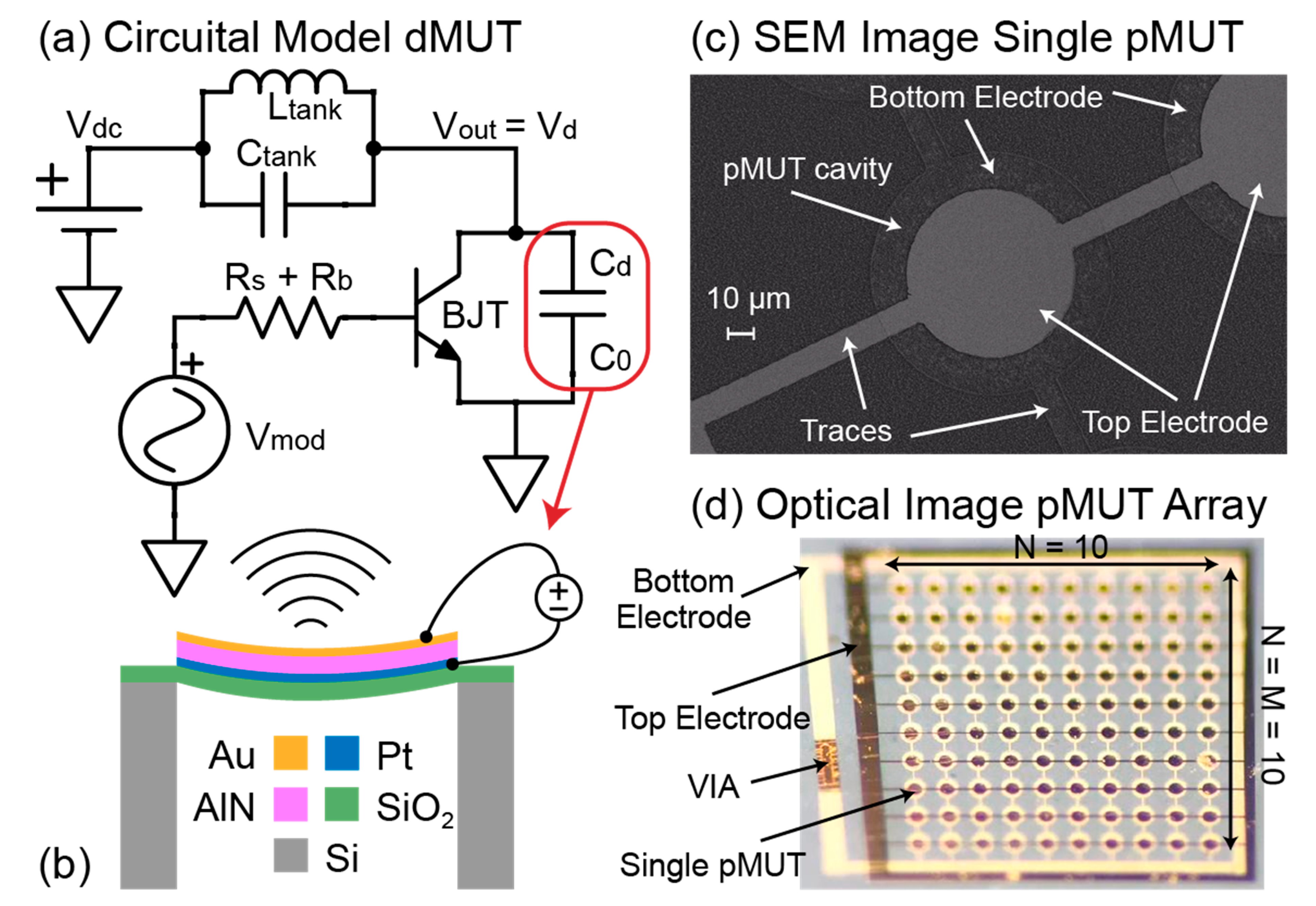
Ultrasonic transducers are devices that are able to generate ultrasonic waves and propagate them in either air or water-like media (water, de-ionized water, silicone oil, castor oil, tissue phantom or human tissue). In particular, Micromachined Ultrasonic Transducers (MUTs) can be of two types: capacitive MUTs or cMUTs [1,2] and piezoelectric MUTs or pMUTs [3,4]. While both devices are actuated with an electric field, the pMUTs take advantage of the piezoelectric properties as well. The generation of the ultrasonic waves is due to the displacement of a membrane that consists of a piezoelectric layer, sandwiched between two electrodes, and a structural layer, all suspended on top of a cavity trenched on the handling wafer Figure 1b. The membrane displaces due to the inverse piezoelectric effect activated by the electric field of an AC voltage signal applied between the two electrodes. The higher the voltage, the higher the membrane displacement, and thus the output pressure generated by the pMUT. These devices can be used for a wide variety of applications, such as fingerprint sensors [5,6,7], range finders [8,9,10], power transfer [11,12,13], medical imaging [14,15,16,17,18], and more recently, for intra-body and underwater communication [19,20,21,22]. In all of the above applications, pMUTs are used as transmitting and receiving elements of ultrasound pressure. In order to extend the range of transmission and minimize the power consumption, there is the need for more sensitive elements. This translates into higher output pressure given a fixed input voltage (transmitter sensitivity) and higher received voltage given a fixed input pressure (receiver sensitivity). The most commonly used technique to increase the sensitivity is to combine single pMUTs into arrays and to make the latter work as a single radiating element [23]. This allows to transmit the combined pressure and to receive the combined charge of all the individual pMUTs in the array. In this work, we propose a complementary driving circuit that can significantly increase the transmitting sensitivity of a pMUT array without any modification of the array itself.

Figure 1.
(a) Circuital model of the dMUT system. (b) Design of a single pMUT. (c) Scanning Electron Microscope (SEM) image of a single pMUT [19]. (d) Optical image of a fabricated pMUT array [19].
The driving circuit proposed in this work and shown in Figure 1a is able to generate high AC voltages on top of a pMUT array starting with low voltage input signals. This allows to maintain compatibility with existing electronics, such as CMOS Integrated Circuits (IC), off-the-shelf microcontrollers, and Field Programmable Gate Arrays (FPGA). Moreover, the driving circuit allows to directly feed the information to be transmitted into the pMUT array with an ON/OFF keying modulation scheme. The data to be transmitted can be generated as a bitstream with a commercially available microcontrollers and directly fed at the input of the driving circuit, thanks to the low voltage input signal requirements. This technique is known as direct modulation and it has been demonstrated in the past for RF applications [24,25,26,27,28]. The novelty in this paper consists on applying the direct modulation to ultrasonic transducers (dMUT) and simultaneously increasing the transmission sensitivity as initially demonstrated in [29]. In this paper the following are detailed: working principle of the dMUT, gain and energy consumption optimization based on several parameters of the system and experimental results of its first implementation.
2. Materials and Methods
2.1. System Design of the dMUT
The dMUT circuit consists of an NPN Bipolar Junction Transistor (BJT), an LC filter tank and a driving capacitance, as shown in Figure 1a. The BJT is biased through a base resistance Rb with an AC modulation signal of amplitude Vm and frequency fm. The amplitude of the modulation signal is such that it drives the BJT in the cut-off (Vm = 0 V) and saturation (Vm = 1 V) regions, thus making it behave as a switch. The emitter of the BJT is connected to ground while its collector is connected to both the LC filter tank and the driving capacitance Cdrive. This capacitance represents a generic transducer that is modeled with a static capacitance and is voltage driven. While the dMUT can drive a generic ultrasound transducer, in this work we envision that the Cdrive is either a single pMUT’s capacitance or the total capacitance of a pMUT array. While the Cdrive is connected to ground, thus appearing between the collector and the emitter of the BJT, the LC tank is biased with a DC voltage source Vdc. This source allows to keep energy stored in the tank’s filter, which consists of a capacitance Ctank and an inductance Ltank. Because it is acting as a switch, the BJT turns the connection between the LC tank and the Cdrive ON and OFF. In particular, in the ON-state (or saturation region) the BJT creates a current path between the collector and emitter, thus shorting the Cdrive to ground, allowing it to discharge the stored energy or radiate in the case of a pMUT device. On the other hand, when going back to the OFF state (or cut-off region), the BJT has no more current flowing and the Cdrive is suddenly connected to the LC tank, ready to re-charge again. If the tank capacitance is much smaller than the driving one (e.g., Ctank ≤ Cdrive/10), then we are generating an abrupt energy imbalance, that will result into the formation of a high amplitude and short duration AC pulse. This approach works because the quality factor of the pMUT array in water or tissue (QpMUT ≈ 1–5) is much smaller compared to the quality factor of the inductance of the LC tank (Qtank ≈ 40–50): QpMUT << Qtank. This kind of AC pulse is ideal for driving ultrasonic transducers for several reasons: it increases the transmitted pressure and the operation range, it improves Signal-to-Noise Ratio (SNR), and at the same time it reduces the power consumption compared to driving the pMUT with continuous waves (CW). The generated pulse intensity can also be optimized by tuning the resonance frequency of the LC tank ftank with respect to the resonance frequency of the pMUT array fpMUT. Finally, given the switching operation of the BJT, the input AC modulation signal can be synthesized as a square wave and encode an ON/OFF keying communication scheme, allowing the transmission of “0 s” and “1 s” directly through the dMUT system on top of an ultrasonic transducer.
2.2. Modeling of an Individual pMUT
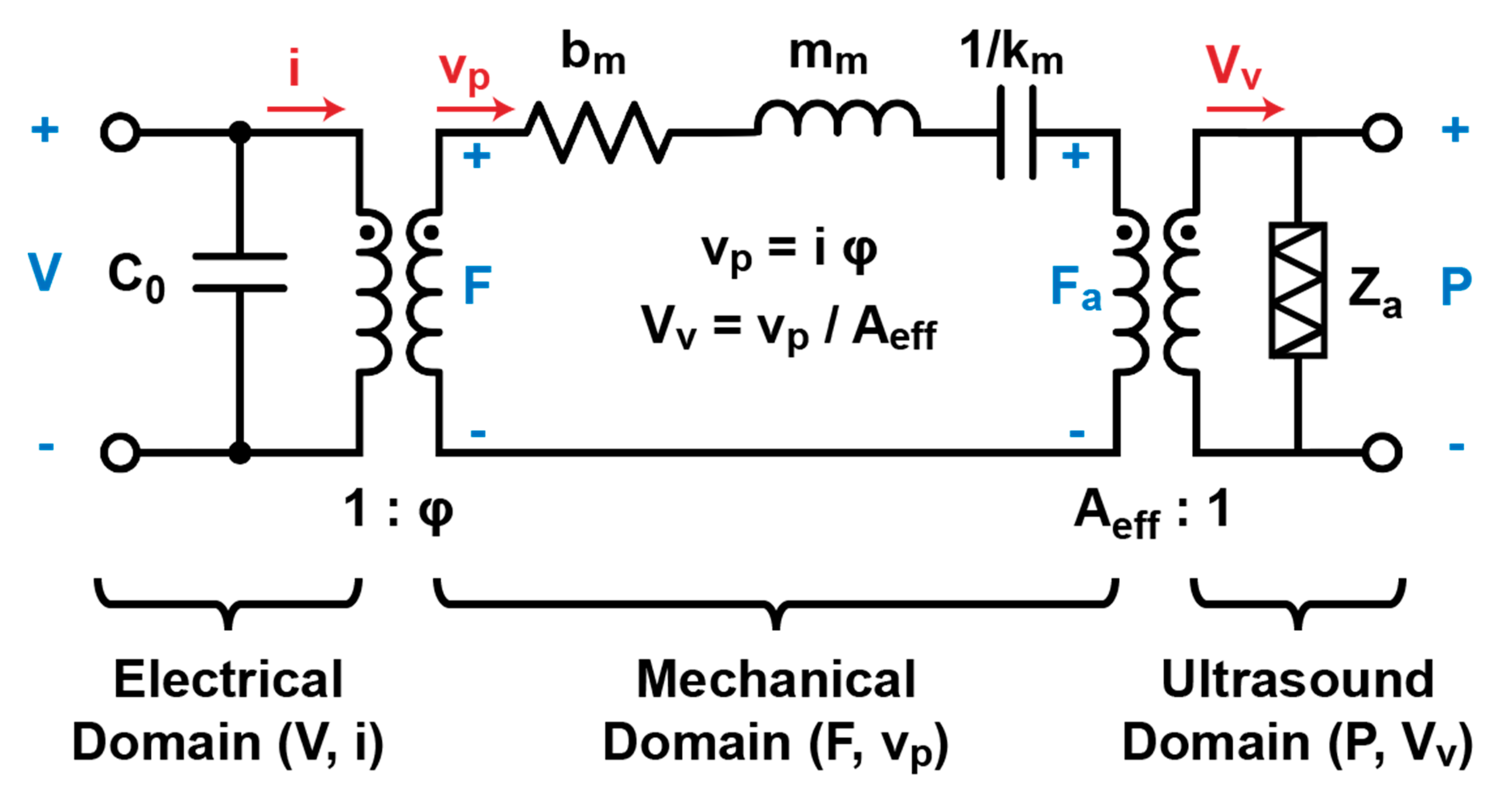
In order to fully evaluate the performances of the dMUT system and its energy consumption, we need to simulate the full pMUT circuital model. Here we are choosing to use the Mason model [30,31,32] as shown in Figure 2 that models the electrical, mechanical, and ultrasound domain. The electrical domain contains the static capacitance C0 is mainly responsible for the voltage gain of the dMUT. Following we have the motional parameters such as the mechanical damping bm, the motional mass mm, and the motional stiffness km, which will set the mechanical resonance frequency of the pMUT membrane and the current consumption. Finally, in the acoustic domain we have the acoustic impedance Za which is responsible for the ultrasonic radiation. The real part of this term is responsible for more current consumption. More information about the modeling of the pMUT is shown in previous publication [33].

Figure 2.
Mason circuital model of the pMUT [30,31,32]. Electrical, mechanical, and ultrasound domains are fully modeled. On one hand, the electrical domain is transformed into the mechanical domain through an ideal transformer of ratio 1:ϕ which is the electro-mechanical coupling factor. On the other hand, the mechanical domain is transformed into the ultrasound domain trough the effective area Aeff:1 which is 1/3 of the area of the pMUT membrane.
2.3. Simulation of the dMUT
The full dMUT system simulation is shown in this section. The values used are presented in Table 1 together with the relationships between those parameters as discussed in the previous section. Furthermore, novel characterization metrics will be defined to evaluate the performance of a dMUT system. The simulation results of the dMUT output voltage Vdrive over time is shown in Figure 3.

Table 1.
Parameters summary of the dMUT system together with their typical values (unless otherwise specified in the paper) and their description.
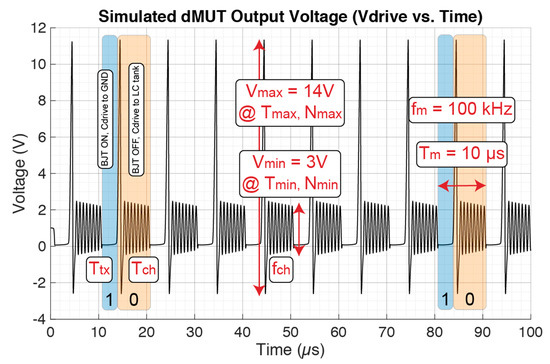
Figure 3.
Simulation of the dMUT system with the values from Table 1. The blue region of period Ttx indicates the transmission region there the BJT is ON and Cdrive is connected to ground. The orange region of period Tch instead indicates the charging region where the BJT is OFF and Cdrive is connected to the LC tank.
Given a modulation frequency of fm = 100 kHz, the resulting modulation period will be Tm = 1/fm = 10 μs. The Tm is highlighted in the figure with a “blue” or transmission region, and an “orange” or charging region. In the transmission region the BJT is ON and Cdrive is connected to ground for a period Ttx ≈ 3 μs. During this time, the capacitance discharges, or in the case of a pMUT, it radiates the power outside the system, thus we have ultrasonic transmission, which can be encoded with an “1” bit. On the other hand, in the charging region the BJT is OFF and Cdrive is connected to the LC tank for a period of Tch ≈ 7 μs. During this time, energy stored in the LC filter flows into the driving capacitance or pMUT, thus charging it, which can be encoded with a “0” bit. Due to an abrupt capacitance and frequency change when the LC tank connects to the Cdrive, there is the generation of a short time and high amplitude AC pulse, which in this case is Vmax = 14 V for a period of Tmax ≈ 1 μs and a number of cycles Nmax = 1. Following this short pulse, the signal’s intensity decays to a lower amplitude of Vmin = 3 V for a period of Tmin ≈ 6 μs and a number of cycles of Nmin = 8. These parameters and their dependencies are going to be analyzed further in the paper.
Now we can define some time and intensity-based performance metrics for the dMUT system. First, we have the transmission Duty Cycle (DT) defined as following:
Based on the values obtained from the simulation the DT ≈ 30%. Second, the Pulse Time Generation (PTR) ratio is defined relating the decay period to the charging period:
Based on the values obtained from the simulation the PTR ≈ 17%. Third, the communication bandwidth (BW) for an ON/OFF keying modulation scheme is defined as follows:
At this point, the pulse amplitude gain with respect to the input modulation voltage, which is the gain of the system, can be defined for each modulation frequency fmod as:
Based on the values obtained from the simulation the Amax ≈ 14 V. For the pulse amplitude gain a logarithmic value G can be defined as:
Based on the value of Amax, G ≈ 23 dB. Finally, the charging operation frequency fch which is set by the combined Cdrive and the Ctank can be identified as:
3. Results
3.1. Energy Consumption
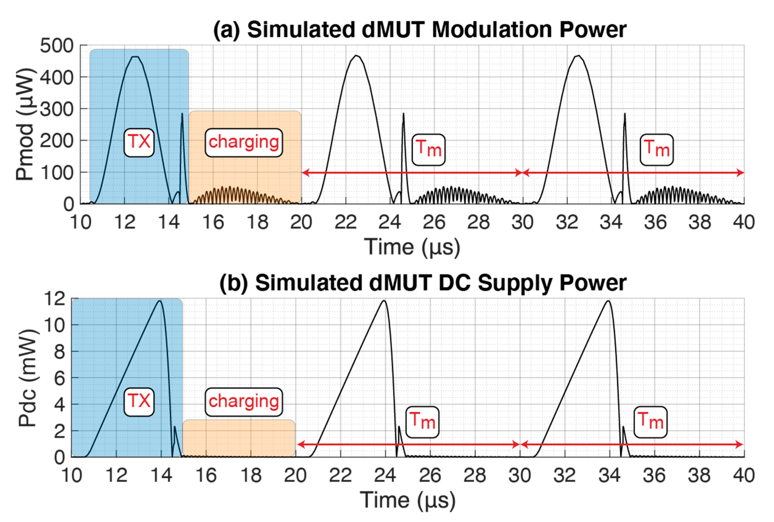
In this section we are going to compute the energy consumption of the dMUT system and compare it with the equivalent case of driving and modulating the pMUT array with the standard continuous wave (CW) approach. As shown in Figure 1a, the dMUT has only two voltage sources, Vmod and Vdc, which will set the power consumption for the circuit. In Figure 4 we are showing the dMUT power consumption when driving a 20 × 20 array. Since the waves are distorted, we are going to integrate the power over a modulation period Tm in order to determine the energy consumption, as following:
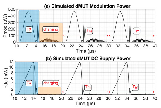
Figure 4.
Power consumption of the dMUT system with the values from Table 1. (a). Power generated by the AC sinusoidal input modulation signal. (b). Power generated by the DC bias voltage signal.
The resulting modulation energy is Emod ≈ 1.15 nJ and the DC supply energy is Edc ≈ 24.85 nJ, for a total energy of Etot ≈ 26 nJ to drive the entire array. If normalized by the number of elements, we obtain a required energy per driven pMUT of . At this point we compare the energy consumption with the CW approach shown in Figure 5.
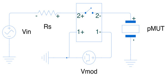
Figure 5.
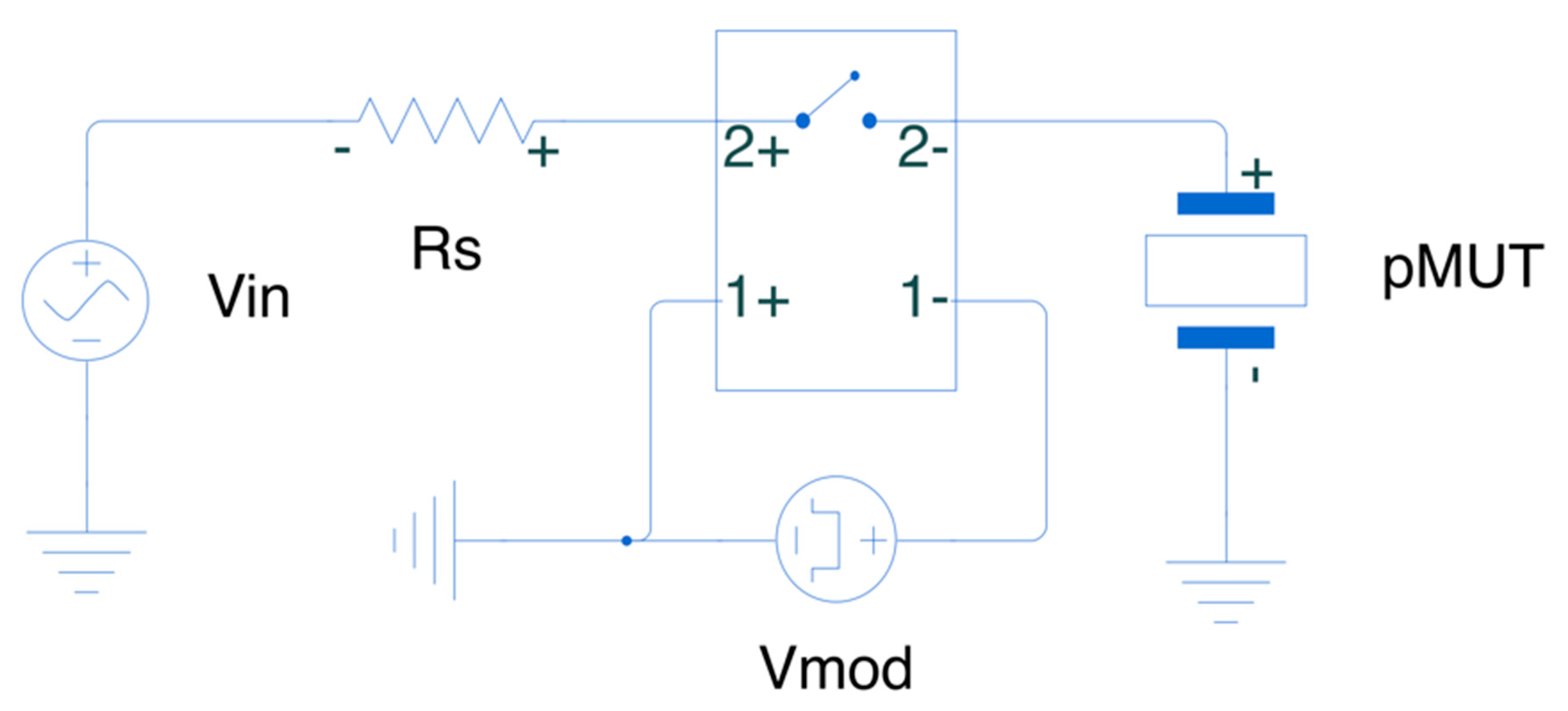
Continuous wave driving of the pMUT array with and ideal switch to implement the ON/OFF keying modulation.
In order to have the same performance as the dMUT, the CW circuit needs to produce the same peak-to-peak voltage on the driven pMUT. In this case Vpp = 14 V as shown in Figure 3, thus we are going to assign this value to Vin = 14 V (or 7 V AC source) in Figure 5 operating at the resonance frequency of the pMUT array, fin = fpMUT. On the other hand, the voltage driven switch is ideal in the simulation, thus Vmod has no power consumption. However, the Vmod frequency of fmod = 100 kHz will set the period T = 10 μs, interval for which Vin is on, thus setting its energy consumption.
By simulating the pMUT Mason model as shown in Figure 2, we obtain that the current consumption for a single pMUT is Iin ≈ 4 μA. For the switch instead, we can assume a low power consumption Single Pole Single Throw (SPST) such as Pmod ≈ 1 μW (ADI ADG902), resulting in an energy consumption Emod ≈ 10 pJ. Finally, the input energy can be computed over the modulation period resulting being Ein ≈ 107 pJ, thus the total energy consumption per pMUT is . This makes the dMUT system 45% more efficient in terms of energy consumption, or the CW systems is 80% more energy demanding.
3.2. System Optimization
This section focuses on how the dMUT system scales when changing the driving capacitance. As this represents the equivalent static capacitance of a pMUT array, the scaling corresponds to changing the total number of individual pMUTs in the array. Furthermore, how to optimize the system performance, gain and energy consumption will be shown in terms of input modulation frequency fm, capacitance ratio CR, frequency ratio between pMUT frequency and LC tank filter frequency FR and DC bias of the filter Vdc. Each of those parameters will be swept once at a time while all the other parameters in the dMUT system are kept constant as in Table 1.
3.2.1. Modulation Frequency (fm)
Figure 6 shows the dMUT system gain and energy consumption while sweeping the modulation frequency fm. This allows to choose the optimal fm of operation that ultimately sets the data-rate in an ON/OFF modulation communication scheme. The maximum gain Gmax = 21 dB is obtained at fm = 150 kHz as shown in Figure 6a. In order to optimize the energy consumption per modulation period (or every two transmitted bits), the operation of the system is extended to two regions R3dB and R6dB, corresponding to 3 dB and 6 dB distance from Gmax respectively. From Figure 6b it can be seen that the energy consumption reaches a maximum Emax = 24 nJ at fm = 100 kHz and then it decreases with an inverse quadratic law while increasing linearly the fm. By operating at the far right of the two operation regions defined above, the energy is reduced to E3dB = 3 nJ and E6dB = 1 nJ at fm = 450 kHz and fm = 600 kHz.
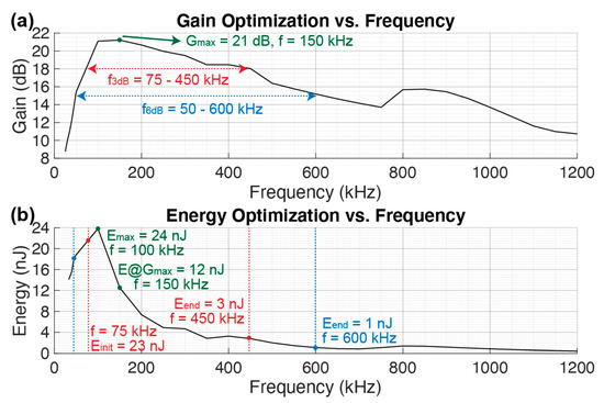
Figure 6.
Gain (a) and energy (b) optimization over a sweep on the modulation frequency fm. The remaining values are maintained constant as in Table 1.
In order to understand the physical reason behind the energy decrease with increased frequency, the power consumption curve in Figure 4 needs to be studied. First of all, since the considered energy is the energy per modulation period Tm, by increasing fm we reduce the Tm, thus when integrating to compute the energy, this will be lower. Second of all, there will be a major integration reduction of the area in the transmission region Ptx, since we are shorting the BJT faster, and thus it consumes less power and energy.
3.2.2. Array Dimension (N × N)
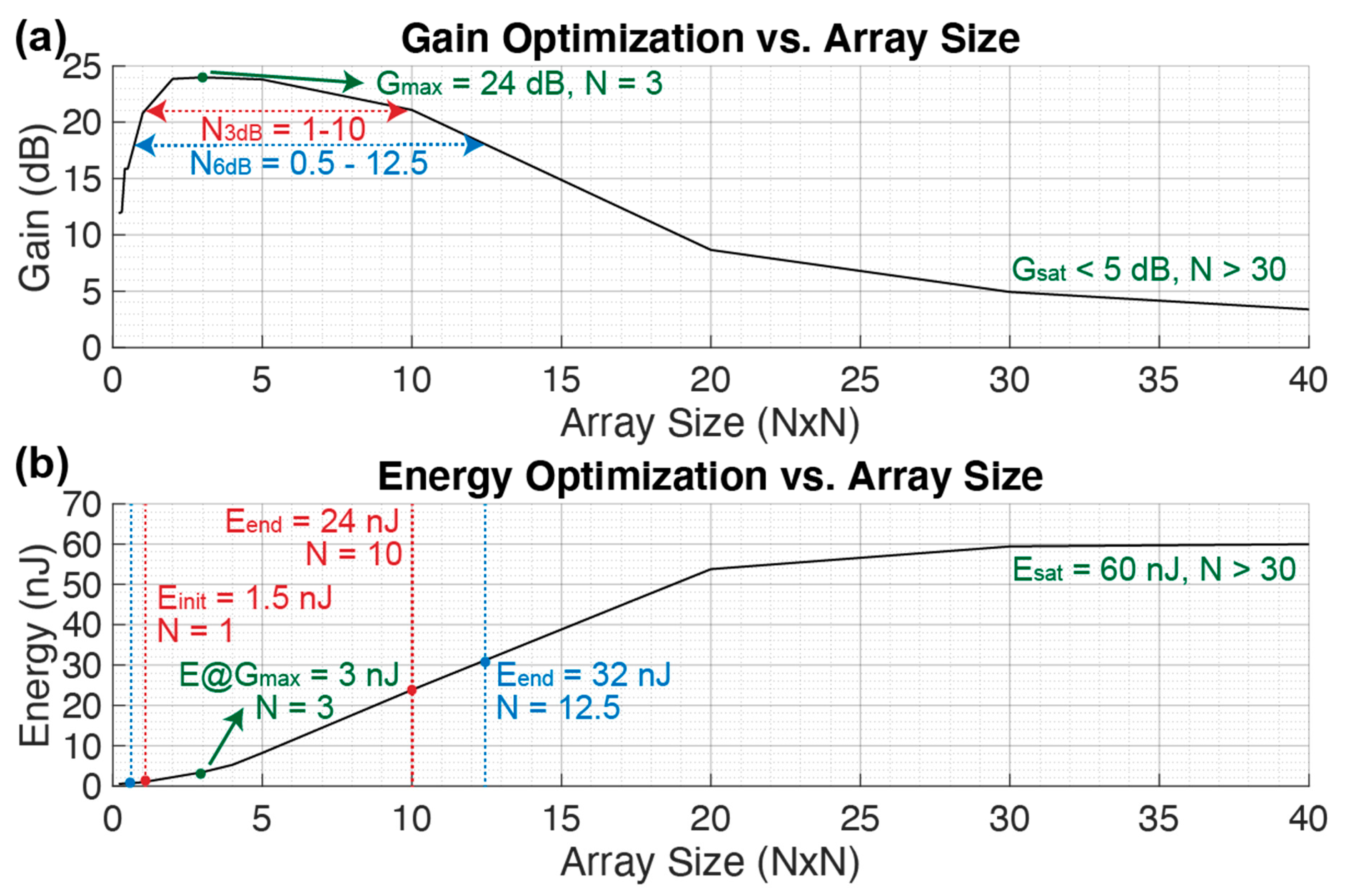
Figure 7 shows the gain and energy consumption while sweeping the array size Ntot = N · M = N2 for N = M. The array size sets the total driving capacitance based on the evaluated capacitance of a single pMUT element Cd = Ntot · C0. On one hand, Figure 7a shows a maximum gain of Gmax = 24 dB when the array size is N = 3. On the other hand, Figure 7b shows a linear energy consumption increase while increasing N. By extending the operation regions to R3dB and R6dB, instead of optimizing the energy consumption, the maximum energy while operating within the same regions can be determined. In particular the maximums are E3dB = 24 nJ and E6dB = 32 nJ for N = 10 and N = 12.5. Finally, when N > 30, the gain reaches a saturation level Gmin < 5 dB and a saturation of the energy consumption Esat = 60 nJ.
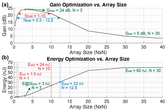
Figure 7.
Gain (a) and energy (b) optimization over a sweep on the array size NxN. The remaining values are maintained constant as in Table 1.
In this case, the energy consumption intuitively increases with the number of elements to drive since the system will require more current to drive each pMUT. Furthermore, once the gain reaches a saturation level Gsat < 5 dB for N > 30, an energy saturation Esat = 60 nJ can be noticed, which would equal the energy required to drive the Cd without the dMUT since the circuit has become inefficient.
3.2.3. Capacitance Ratio (CR)
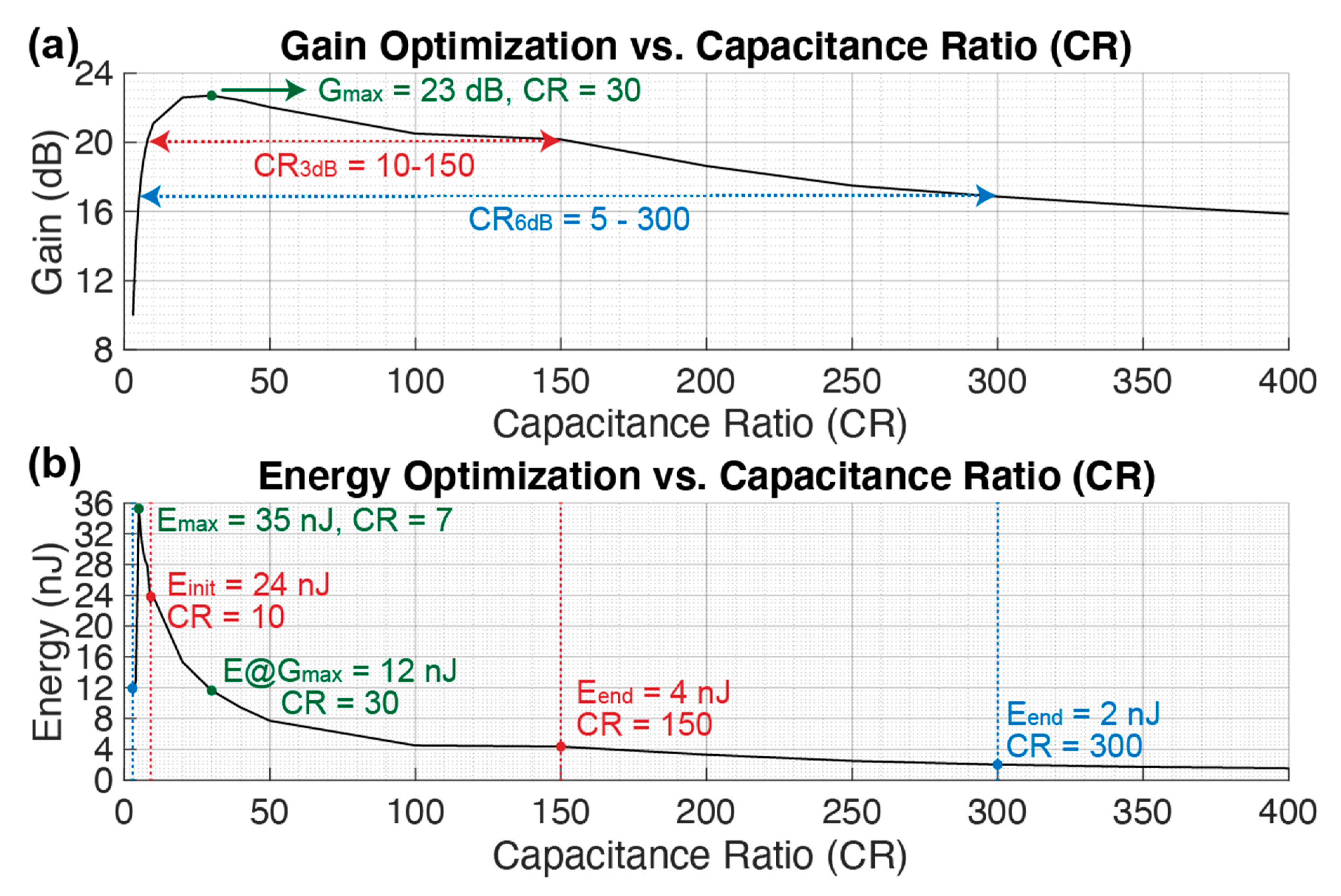
In Figure 8 the gain and energy consumption are shown while sweeping the capacitance ratio CR. By increasing the CR, the dMUT gain reaches a maximum of Gmax = 23 dB at CR = 30 and after this point the gain decreases linearly as shown in Figure 8a. Working at higher CR helps to decrease the energy consumption as shown in Figure 8b. In particular, after reaching a maximum of Emax = 35 nJ at CR = 7, the energy decreases with an inverse quadratic law while increasing CR linearly. At this point, by choosing a point at the end of the operation regions R3dB and R6dB, a minimum in the energy consumption per modulation period is seen, E3dB = 4 nJ and E6dB = 2 nJ respectively at CR = 150 and CR = 300.
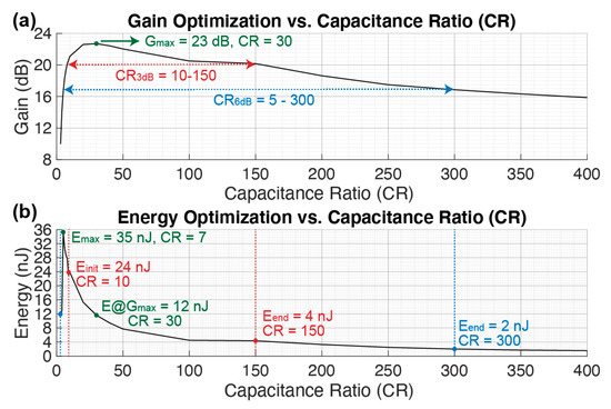
Figure 8.
Gain (a) and energy (b) optimization over a sweep on the capacitance ratio CR. The remaining values are maintained constant as in Table 1.
The energy consumption finds its maximum when the energy exchange between the LC filter tank and the driving capacitance is not optimal and it requires additional current feeding from the DC voltage source. Once the CR is increased, the filter capacitance Ctank becomes much smaller than the Cd. This permits to charge the Cd with more energy efficiency, explaining the decrease of the energy consumption while increasing CR.
3.2.4. Frequency Ratio (FR)
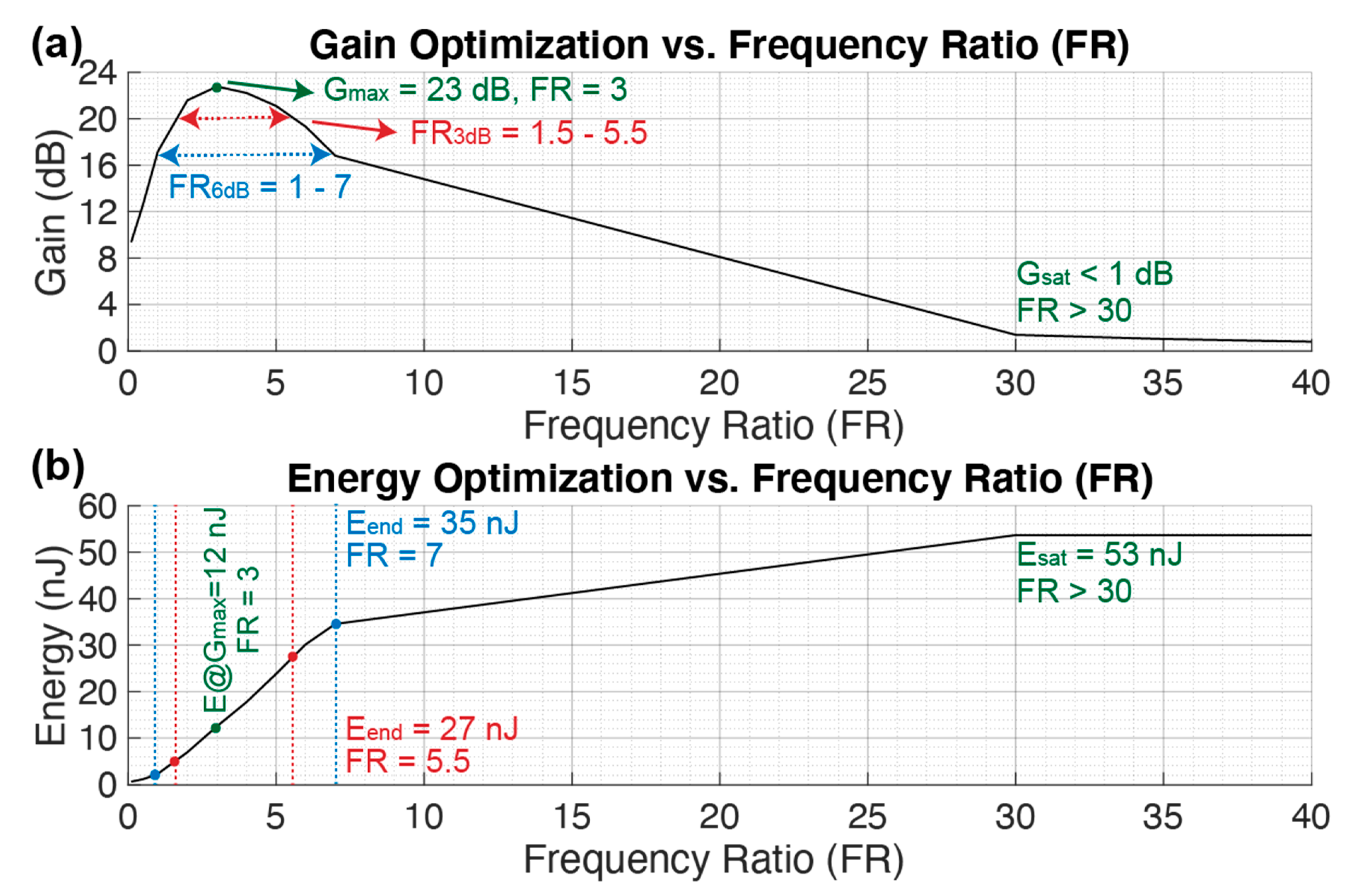
Figure 9 shows the gain and energy consumption while sweeping the frequency ratio FR. The gain reaches a maximum of Gmax = 23 dB at FR = 3 and then decreases linearly until FR = 30, after which there is a gain saturation Gsat < 1 as shown in Figure 9a. Instead, the energy consumption increases with a square root law while increasing the FR linearly. The minimum energy consumption is obtained at the beginning of the R3dB and R6dB resulting in E3dB = 5 nJ and E6dB = 2 nJ respectively at FR = 1.5 and FR = 1. In this last parameter sweep, the energy increases while increasing FR. This physically means that the LC tank filter is operating at higher frequency with respect to the resonance frequency of the pMUT array fpMUT, thus it requires more energy for the filter to operate and charge up. Finally, the energy reaches a saturation level Esat = 53 nJ when FR > 30, similar to the N sweep in Figure 7. This happens because the gain also reaches a saturation Gsat < 1, making the dMUT system very inefficient, thus the resulting energy consumption is the one that is required to drive the Cd without the dMUT circuit.
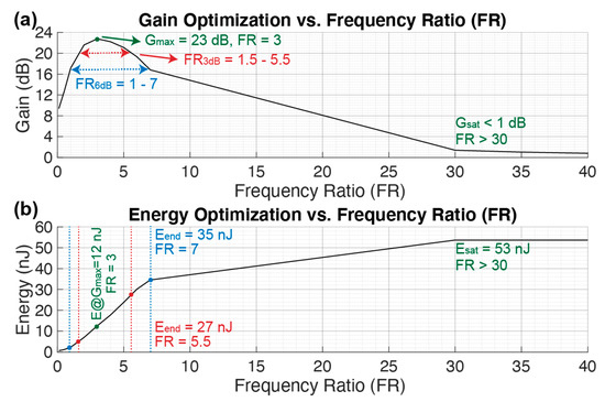
Figure 9.
Gain (a) and energy (b) optimization over a sweep on the frequency ratio FR. The remaining values are maintained constant as in Table 1.
A summary of the values obtained from the optimization simulations are shown in Table 2.

Table 2.
Summary of dMUT gains and energy optimization parameters and their values.
3.2.5. High Performance dMUT
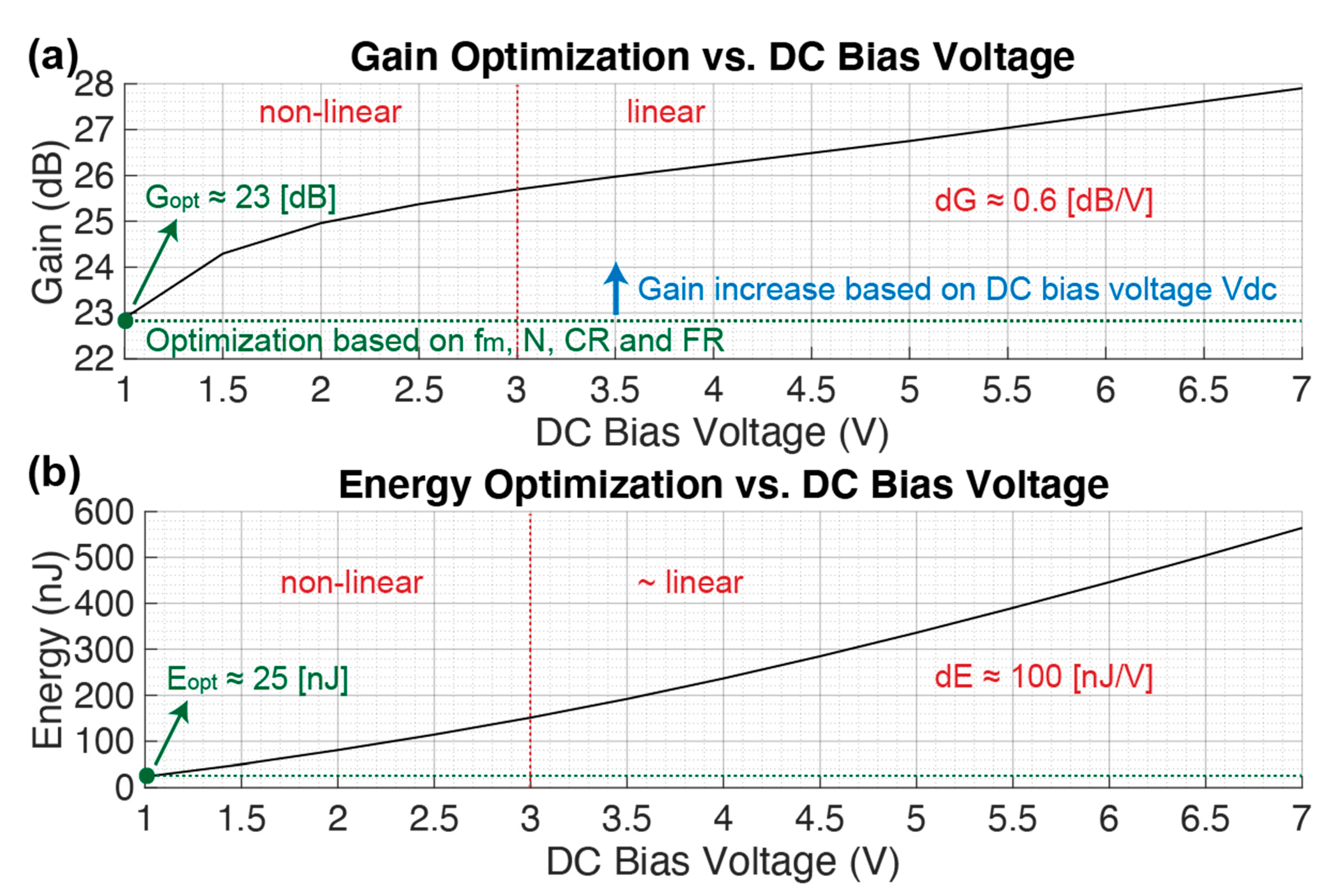
The previous sections detailed a gain and energy consumption optimization of the dMUT system by exploring the operation ranges for several parameters such as fm, N, CR, and FR while maintaining the remaining parameters constant as in Table 1. In particular, the DC biasing voltage of the LC filter tank was kept to Vdc = 1 V. In this section, a high-performance system is explored which is boosted by an increase in the DC bias. By doing so, the LC tank will be able to store more energy and boost the output voltage on top of the driven capacitance, which is the equivalent capacitance of a pMUT array. In Figure 10 the dMUT gain G for a DC bias range of Vdc = 1–10 V is shown. As it can be noticed, for Vdc = 1 V there is a minimum optimal gain corresponding to the one obtained in the optimization section. By further increasing the bias, the gain increases non-linearly up to Vdc = 3 V and then follows a linear trend. For the linear region we can compute the differential gain increase based on Vdc as following:
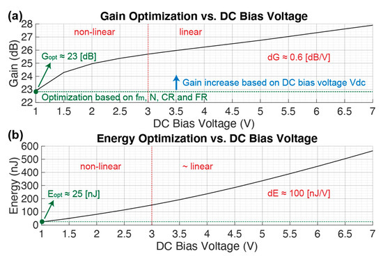
Figure 10.
High performance gain (a) and energy (b) consumption based on the DC biasing voltage Vdc of the LC tank filter. The remaining values are maintained constant as in Table 1.
The gain boosting comes at a large expense in the energy consumption as shown in Figure 10b. As for the gain, the energy has a minimum that comes from the optimization section Eopt = 25 nJ at Vdc = 1 V. The energy consumption follows a non-linear trend up to Vdc < 3 V and then a linear trend. For the linear region we can compute the differential energy increase based on Vdc as following:
Even though the high performance dMUT system is power hungry, it could still be an optimal solution for certain application that allows for large batteries or for wired connections. For example, this could be the case of a power transfer application from an external ultrasonic transducer, which can be wire-connected to drain power, that sends power to a medical device deeply implanted in a human body (>10 cm).
4. Discussion
In this last section the dMUT system is implemented in a Printed Circuit Board (PCB) with off-the-shelf components as shown in Figure 11. On the PCB we can notice the LC filter tank, with a capacitance Ctank and inductance Ltank, the BJT and the base resistance Rb. The chosen BJT is the ComChip MMBTA44-G since it can handle high voltages (>100 V) compared to other transistors. Moreover, the conduction losses can be estimated from the saturation voltage, VCEsat ≈ 55 mV. Base on the current consumption that can range from 1 to 10 mA, the power will be around 55 to 550 μW. Following, the PCB connects through SMA connectors to the DC bias source Vdc, to the pMUT array static capacitance CpMUT or an equivalent driven capacitance Cd, to the input modulation signal Vm that has a series input resistance Rs and to an SMA connecting the BJT’s emitter to ground GND. While this approach can work with a MOSFET, we choose a BJT because it can handle higher voltages on the collector node.
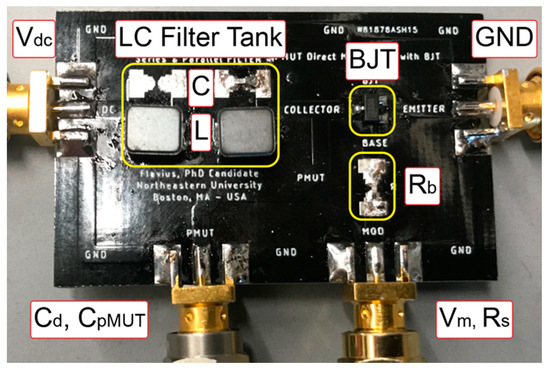
Figure 11.
Printed Circuit Board (PCB) implementation of the dMUT system based on the parameters in Table 1 with the exception of the DC biasing voltage that was increased to Vdc = 7 V for high performance application [29].
In Figure 12 the experimental results of the dMUT system are shown based on the values from Table 1 with the exception of the DC biasing voltage that is increased to Vdc = 7 V for high performance applications. The “green” curve shows the input modulation signal Vm = 1 V at fm = 100 kHz. Further, the “black-dotted” curve shows the simulation of the output voltage generated on top of the driven capacitance of the dMUT array. This curve is a good match with the experimentally measured output voltage indicated by the “blue” curve. The output voltage shows a maximum of Vmax = 84 V when a DC bias of Vdc = 7 V is applied to the LC filter corresponding to a system gain of G = 38.5 dB.
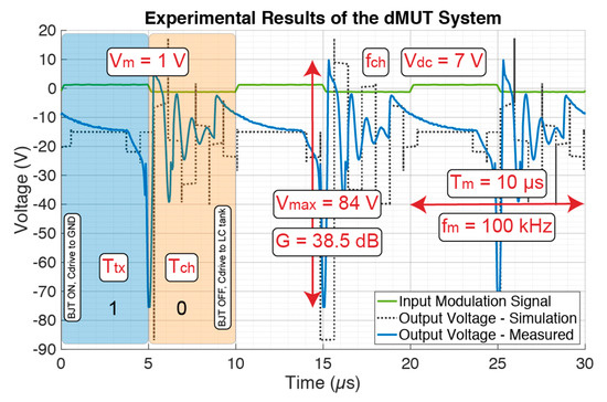
Figure 12.
Experimental results of the dMUT system based on the parameters in Table 1 with the exception of the DC biasing voltage that was increased to Vdc = 7 V for high performance application. The output voltage is compared to the simulation results showing a good matching. The maximum voltage is Vmax = 84 V which corresponds to a system gain of G = 38.5 dB of the dMUT system.
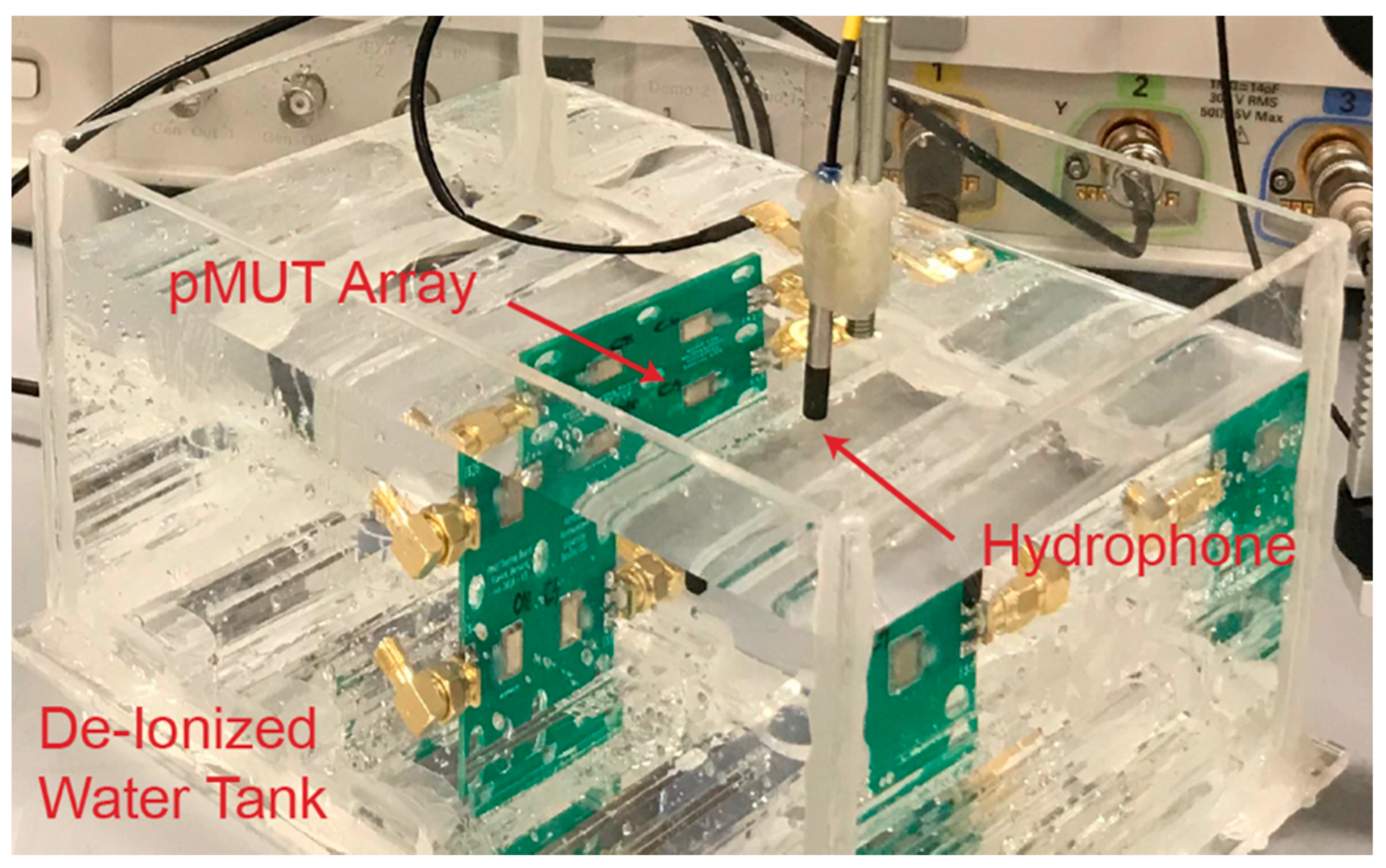
In order to demonstrate the advantage of driving a pMUT array with the dMUT system as opposed to traditional CW, we are going to perform an ultrasonic transmission experiment in a De-Ionized (DI) water tank as shown in Figure 13. The pMUT array is used as a transmitter and is driven either by the dMUT system or by a simple CW system. The received signal is then received and captured by an underwater ultrasonic hydrophone (Teledyne TC4038) and converted into electrical signal. The sensitivity of such device is −228 dB reference to 1 V/μPa, which sets the minimum detectable signal. Translated into electrical signal, this means that the Noise Floor (NF) is NF = 4 μV peak-to-peak, thus the incoming ultrasonic signal needs to generate a signal higher than the NF in order to be detectable.
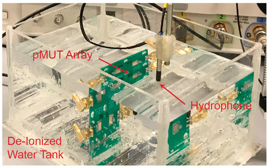
Figure 13.
De-Ionized (DI) water tank for ultrasonic experiment measurements. The transmission is done between a pMUT array and an ultrasonic hydrophone (Teledyne TC4038) for reference. Given the small dimensions of the tank, there will be some interference due to the reflections at the interface, creating a multipath. Absorptions layers can be added to the wall to reduce the multipath phenomena.
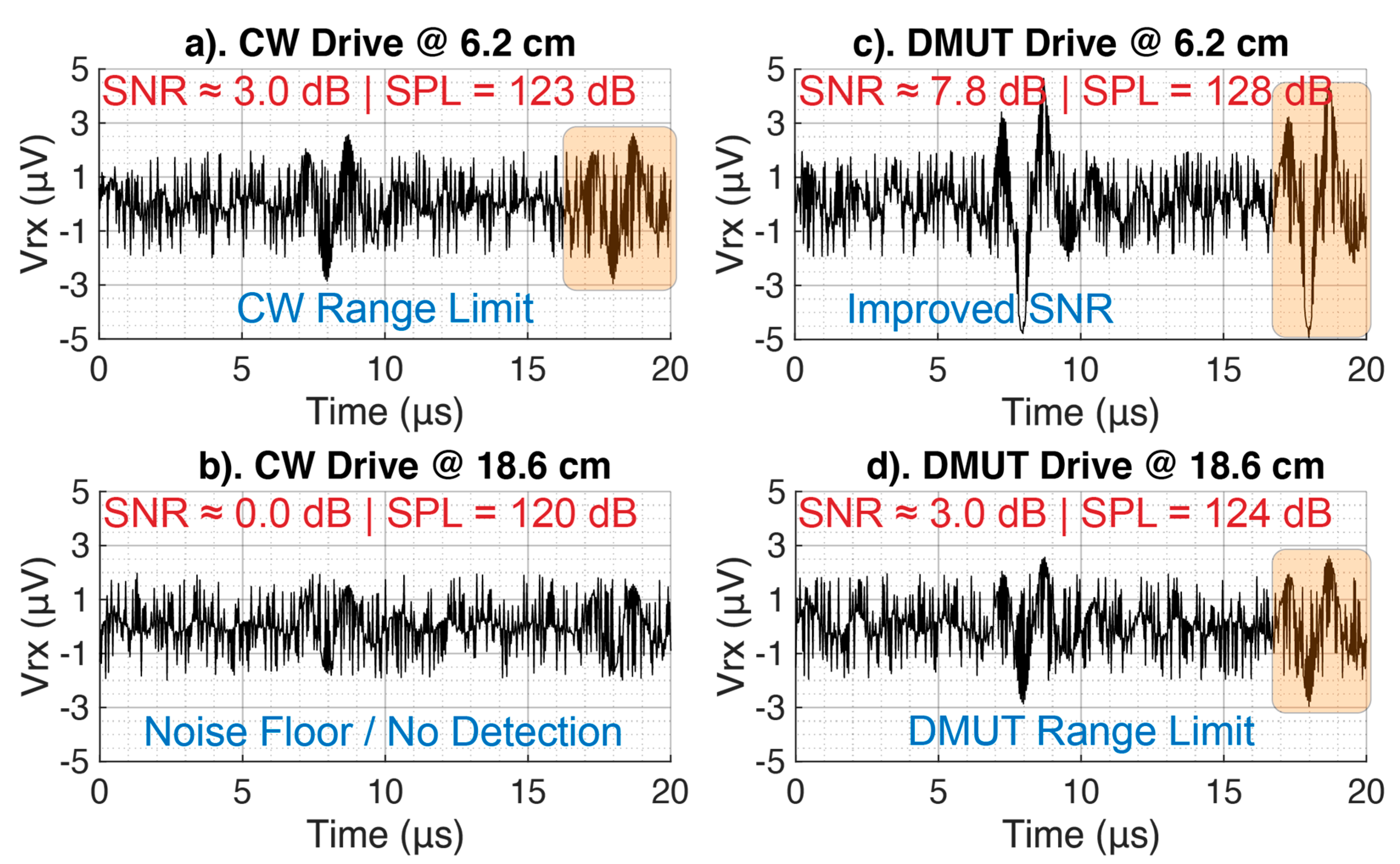
Firstly, we drive the pMUT array in CW with the same energy level of the dMUT system and we identify the maximum reachable Dmax at which we can still detect the incoming ultrasonic signal beyond the NF. In particular we consider a valid signal is this is 3 dB higher than the NF in terms of Sound Pressure Level (SPL), which means that the Signal-to-Noise Ratio (SNR) is SNR ≈ 3 dB. The noise level in terms of SPL is NF ≈ 120 dB. Based on this, a valid signal needs to reach SPL ≥ NF + SNR. In Figure 14 we are sowing the limit of the CW for an array of 20 × 20 pMUT at a distance .
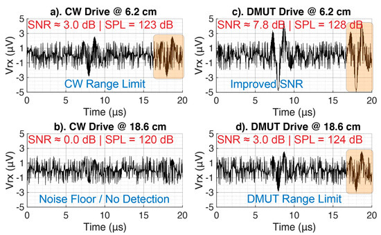
Figure 14.
Measurement results in a water tank. Received signal captured by a Teledyne hydrophone with −228 dB re 1 V/μPa corresponding to a noise floor of NF = 4 μPa. Both systems are driven with the same energy levels. (a) CW drive at 6.3 cm corresponding to the maximum reachable distance where the SNR is at least 3 dB. (b) CW drive at 18.6 cm where the SNR is 0 dB, and the signal is not detectable from the noise. (c) DMUT drive at the same distance as in (a); this new drive approach shows an improvement of the SNR from 3 dB to 7.8 dB for same input energy level. (d) DMUT drive at the same distance as in (b); this new drive approach shows an improvement of the SNR from 0 dB to 3 dB allowing, extending the communication link from 6.2 cm, which is the maximum limit for the CW drive as shown in (a), to 18.6 cm, which is the maximum limit for the DMUT drive as shown in (d), for the same input energy level.
Secondly, we drive the pMUT array with the dMUT system at the same energy level as the CW drive. At the same maximum distance as the CW, the dMUT system shows higher SPL ≈ 128 dB and in particular the SNR ≈ 7.8 dB as shown in Figure 14c. This corresponds to an improvement of 2.8 in dB scale or 3× in linear scale.
Finally, we want to find the range limit for the dMUT drive of the array similar to the CW drive. As shown in the measurements in Figure 14c, the new maximum reachable distance with an SNR ≈ 3 dB is . This corresponds to an improvement in the operation range of 3× fold. For comparison, in Figure 14b we are driving the array with the CW at the maximum distance of the dMUT. As we can see the incoming ultrasonic signal is no longer detectable, thus SNR ≈ 0 dB.
In conclusion the dMUT system was proven to be effective in increasing the transmitting sensitivity of a pMUT array while performing direct modulation of an ON/OFF keying modulation scheme and direct screaming of the bitstream. The main operating circuit of the dMUT was described in terms of its switched LC tank working principle and gain, power and energy metrics were introduced. Optimization was then performed relative to the input modulation frequency, array dimensions (drive capacitance), drive to tank capacitance ratio, and tank to pMUT resonance frequency ratio. Taking this optimization into consideration, an experimental high-performance implementation was shown able to achieve a 38.5 dB gain (a maximum of 84 V for a 1 V input) for a 7 V DC bias and a 100 kHz modulation frequency. This system can work with DC biases below 3 V which can be CMOS compatible. Furthermore, this improved performance comes with 80% less energy consumption compared to traditional CW driving and implementation of the same modulation scheme. Finally, when compared with the same energy levels, the dMUT shows an improvement of 3× of the SNR and the maximum reachable communication range at 3 dB from the noise floor. This work will be further extended in a separate paper to incorporate a full receiver architecture to demodulate the incoming signal from the dMUT and pMUT ultrasonic link. This will make use of an envelope filter, active filtering blocks, and a comparator. In the end, the transmitter and receiver will be interfaced with a microcontroller for data encoding and decoding.
Author Contributions
Conceptualization, F.P., B.H. and C.C.; device design and fabrication, F.P. and B.H.; system integration and validation, F.P.; formal analysis, F.P.; investigation, F.P. and C.C.; resources, M.R.; writing—original draft preparation, F.P.; writing—review and editing, B.H., C.C. and M.R.; supervision, C.C.; project administration, M.R.; funding acquisition, M.R. All authors have read and agreed to the published version of the manuscript.
Funding
This research was funded by the NSF programs MRI-SEANet, grant number 1726512, and NeTS-Small, grant number 1618731.
Data Availability Statement
Data sharing is not applicable to this article.
Conflicts of Interest
The authors declare no conflict of interest.
References
- Ergun, A.S.; Yaralioglu, G.G.; Khuri-Yakub, B.T. Capacitive Micromachined Ultrasonic Transducers: Theory and Technology. J. Aerosp. Eng. 2003, 16, 76–84. Available online: https://ascelibrary.org/doi/abs/10.1061/%28ASCE%290893-1321%282003%2916%3A2%2876%29 (accessed on 23 December 2020). [CrossRef]
- Ergun, A.S.; Huang, Y.; Zhuang, X.; Oralkan, Ö.; Yaralıoglu, G.G.; Khuri-Yakub, B.T. Capacitive Micromachined Ultrasonic Transducers: Fabrication Technology. IEEE Trans. Ultrason. Ferroelectr. Freq. Control 2005, 52, 2242–2258. [Google Scholar] [PubMed]
- Akasheh, F.; Fraser, J.D.; Bose, S.; Bandyopadhyay, A. Piezoelectric micromachined ultrasonic transducers: Modeling the influence of structural parameters on device performance. IEEE Trans. Ultrason. Ferroelectr. Freq. Control 2005, 52, 455–468. [Google Scholar] [CrossRef] [PubMed]
- Muralt, P.; Ledermann, N.; Paborowski, J.; Barzegar, A.; Gentil, S.; Belgacem, B.; Petitgrand, S.; Bosseboeuf, A.; Setter, N. Piezoelectric micromachined ultrasonic transducers based on PZT thin films. IEEE Trans. Ultrason. Ferroelectr. Freq. Control 2005, 52, 2276–2288. [Google Scholar] [CrossRef] [PubMed]
- Tang, H.; Lu, Y.; Fung, S.; Tsai, J.M.; Daneman, M.; Horsley, D.A.; Boser, B.E. Pulse-echo ultrasonic fingerprint sensor on a chip. In Proceedings of the 2015 Transducers—2015 18th International Conference on Solid-State Sensors, Actuators and Microsystems, TRANSDUCERS 2015, Anchorage, AK, USA, 21–25 June 2015; Institute of Electrical and Electronics Engineers Inc.: New York, NY, USA, 2015; pp. 674–677. [Google Scholar]
- Horsley, D.A.; Lu, Y.; Tang, H.Y.; Jiang, X.; Boser, B.E.; Tsai, J.M.; Ng, E.J.; Daneman, M.J. Ultrasonic fingerprint sensor based on a PMUT array bonded to CMOS circuitry. In Proceedings of the IEEE International Ultrasonics Symposium, IUS, Tours, France, 18–21 September 2016; IEEE Computer Society: Piscataway, NJ, USA, 2016. [Google Scholar]
- Jiang, X.; Tang, H.Y.; Lu, Y.; Ng, E.J.; Tsai, J.M.; Boser, B.E.; Horsley, D.A. Ultrasonic Fingerprint Sensor with Transmit Beamforming Based on a PMUT Array Bonded to CMOS Circuitry. IEEE Trans. Ultrason. Ferroelectr. Freq. Control 2017, 64, 1401–1408. [Google Scholar] [CrossRef] [PubMed]
- Liu, X.; Chen, X.; Le, X.; Xu, Z.; Wu, C.; Xie, J. A High-Performance Square pMUT for Range-finder. In Proceedings of the NEMS 2018—13th Annual IEEE International Conference on Nano/Micro Engineered and Molecular Systems, Singapore, 22–26 April 2018; Institute of Electrical and Electronics Engineers Inc.: New York, NY, USA, 2018; pp. 115–118. [Google Scholar]
- Rozen, O.; Block, S.T.; Mo, X.; Bland, W.; Hurst, P.; Tsai, J.M.; Daneman, M.; Amirtharajah, R.; Horsley, D.A. Monolithic MEMS-CMOS ultrasonic rangefinder based on dual-electrode PMUTs. In Proceedings of the IEEE International Conference on Micro Electro Mechanical Systems (MEMS), Shanghai, China, 24–28 January 2016; Institute of Electrical and Electronics Engineers Inc.: New York, NY, USA, 2016; pp. 115–118. [Google Scholar]
- Zhou, Z.; Yoshida, S.; Tanaka, S. Monocrystalline PMNN-PZT thin film ultrasonic rangefinder with 2 m range at 1 volt drive. In Proceedings of the TRANSDUCERS 2017—19th International Conference on Solid-State Sensors, Actuators and Microsystems, Kaohsiung, Taiwan, 18–22 June 2017; Institute of Electrical and Electronics Engineers Inc.: New York, NY, USA, 2017; pp. 167–170. [Google Scholar]
- Basaeri, H.; Yu, Y.; Young, D.; Roundy, S. Acoustic power transfer for biomedical implants using piezoelectric receivers: Effects of misalignment and misorientation. J. Micromech. Microeng. 2019, 29, 084004. Available online: https://iopscience.iop.org/article/10.1088/1361-6439/ab257f (accessed on 14 November 2020). [CrossRef]
- Mehdizadeh, E.; Piazza, G. AlN on SOI pMUTs for ultrasonic power transfer. In Proceedings of the IEEE International Ultrasonics Symposium, IUS, Washington, DC, USA, 6–9 September 2017; IEEE Computer Society: Piscataway, NJ, USA, 2017. [Google Scholar]
- Herrera, B.; Pop, F.; Cassella, C.; Rinaldi, M. AlN PMUT-based Ultrasonic Power Transfer Links for Implantable Electronics. In Proceedings of the 2019 20th International Conference on Solid-State Sensors, Actuators and Microsystems and Eurosensors XXXIII, TRANSDUCERS 2019 and EUROSENSORS XXXIII, Berlin, Germany, 23–27 June 2019; Institute of Electrical and Electronics Engineers Inc.: New York, NY, USA, 2019; pp. 861–864. [Google Scholar]
- Dausch, D.E.; Gilchrist, K.H.; Carlson, J.R.; Castellucci, J.B.; Chou, D.R.; Von Ramm, O.T. Improved pulse-echo imaging performance for flexure-mode pMUT arrays. In Proceedings of the IEEE Ultrasonics Symposium, San Diego, CA, USA, 11–14 October 2010; pp. 451–454. [Google Scholar]
- Qiu, Y.; Gigliotti, J.; Wallace, M.; Griggio, F.; Demore, C.; Cochran, S.; Trolier-McKinstry, S. Piezoelectric Micromachined Ultrasound Transducer (PMUT) Arrays for Integrated Sensing, Actuation and Imaging. Sensors 2015, 15, 8020–8041. Available online: http://www.mdpi.com/1424-8220/15/4/8020 (accessed on 23 December 2020). [CrossRef] [PubMed]
- Akhbari, S.; Sammoura, F.; Shelton, S.; Yang, C.; Horsley, D.; Lin, L. Highly responsive curved aluminum nitride PMUT. In Proceedings of the IEEE International Conference on Micro Electro Mechanical Systems (MEMS), San Francisco, CA, USA, 26–30 January 2014; Institute of Electrical and Electronics Engineers Inc.: New York, NY, USA, 2014; pp. 124–127. [Google Scholar]
- Yang, Y.; Tian, H.; Wang, Y.-F.; Shu, Y.; Zhou, C.-J.; Sun, H.; Zhang, C.H.; Chen, H.; Ren, T.L. An Ultra-High Element Density pMUT Array with Low Crosstalk for 3-D Medical Imaging. Sensors 2013, 13, 9624–9634. Available online: http://www.mdpi.com/1424-8220/13/8/9624 (accessed on 23 December 2020). [CrossRef]
- Smyth, K.M.; Sodini, C.G.; Kim, S.G. High electromechanical coupling piezoelectric micro-machined ultrasonic transducer (PMUT) elements for medical imaging. In Proceedings of the TRANSDUCERS 2017-19th International Conference on Solid-State Sensors, Actuators and Microsystems, Kaohsiung, Taiwan, 18–22 June 2017; Institute of Electrical and Electronics Engineers Inc.: New York, NY, USA, 2017; pp. 966–969. [Google Scholar]
- Pop, F.V.; Herrera, B.; Cassella, C.; Chen, G.; Demirors, E.; Guida, R.; Melodia, T.; Rinaldi, M. Novel pMUT-Based Acoustic Duplexer for Underwater and Intrabody Communication. In Proceedings of the 2018 IEEE International Ultrasonics Symposium (IUS), Kobe, Japan, 22–25 October 2018; pp. 1–4. [Google Scholar]
- Pop, F.; Herrera, B.; Zhu, W.; Assylbekova, M.; Cassella, C.; McGruer, N.; Rinaldi, M. Zero-Power Acoustic Wake-Up Receiver based on dMUT Transmitter, pMUTs Arrays Receivers and MEMS Switches for Intrabody Links. In Proceedings of the Transducers-Eurosensors, 2019 IEEE International, Berlin, Germany, 23–27 June 2019. [Google Scholar]
- Sadeghpour, S.; Kraft, M.; Puers, R. Highly Efficient Piezoelectric Micromachined Ultrasound Transducer (PMUT) for Underwater Sensor Networks. In Proceedings of the 2019 20th International Conference on Solid-State Sensors, Actuators and Microsystems and Eurosensors XXXIII, TRANSDUCERS 2019 and EUROSENSORS XXXIII, Berlin, Germany, 23–27 June 2019; Institute of Electrical and Electronics Engineers Inc.: New York, NY, USA, 2019; pp. 162–165. [Google Scholar]
- Sadeghpour, S.; Kraft, M.; Puers, R. PMUTs Array with Dynamic Directivity: A Study of its Underwater Acoustic Power Intensity. In Proceedings of the IEEE International Ultrasonics Symposium, IUS, Kobe, Japan, 22–25 October 2018; IEEE Computer Society: Piscataway, NJ, USA, 2018. [Google Scholar]
- Liu, W.; He, L.; Wang, X.; Zhou, J.; Xu, W.; Smagin, N.; Toubal, M.; Yu, H.; Gu, Y.; Xu, J.; et al. 3D FEM Analysis of High-Frequency AlN-Based PMUT Arrays on Cavity SOI. Sensors 2019, 19, 4450. Available online: https://www.mdpi.com/1424-8220/19/20/4450 (accessed on 23 December 2020). [CrossRef] [PubMed]
- Keller, S.D.; Palmer, W.D.; Joines, W.T. Direct antenna modulation: Analysis, design, and experiment. In Proceedings of the IEEE Antennas and Propagation Society, AP-S International Symposium (Digest), Albuquerque, NM, USA, 9–14 July 2006; pp. 909–912. [Google Scholar]
- Babakhani, A.; Rutledge, D.B.; Hajimiri, A. Transmitter architectures based on near-field direct antenna modulation. IEEE J. Solid-State Circuits 2008, 43, 2674–2692. [Google Scholar] [CrossRef]
- Yao, W.; Wang, Y. Direct antenna modulation-A promise for ultra-wideband (UWB) transmitting. In Proceedings of the IEEE MTT-S International Microwave Symposium Digest, Fort Worth, TX, USA, 6–11 June 2004; pp. 1273–1276. [Google Scholar]
- Fusco, V.F. Direct-signal modulation using a silicon microstrip patch antenna. IEEE Trans. Antennas Propag. 1999, 47, 1025–1028. [Google Scholar] [CrossRef]
- Babakhani, A.; Rutledge, D.; Hajimiri, A. Near-field direct antenna modulation. IEEE Microw. Mag. 2009, 10, 36–46. [Google Scholar] [CrossRef]
- Pop, F.V.; Herrera, B.; Cassella, C.; Rinaldi, M. Direct modulation piezoelectric micro-machined ultrasonic transducer system (dmut). In Proceedings of the 2019 IEEE 32nd International Conference on Micro Electro Mechanical Systems (MEMS), Seoul, Korea, 27–31 January 2019; pp. 61–64. [Google Scholar]
- Huang, C.H.; Gao, H.; Torri, G.B.; Mao, S.; Jeong, Y.; Cheyns, D.; Rochus, V.; Rottenberg, X. Design, modelling, and characterization of display compatible pMUT device. In Proceedings of the 2018 19th International Conference on Thermal, Mechanical and Multi-Physics Simulation and Experiments in Microelectronics and Microsystems, EuroSimE 2018, Toulouse, France, 15–18 April 2018; Institute of Electrical and Electronics Engineers Inc.: New York, NY, USA, 2018; pp. 1–4. [Google Scholar]
- Amar ABen Cao, H.; Kouki, A.B. Modeling and process design optimization of a piezoelectric micromachined ultrasonic transducers (PMUT) using lumped elements parameters. Microsyst. Technol. 2017, 23, 4659–4669. Available online: https://link.springer.com/article/10.1007/s00542-016-3205-8 (accessed on 23 December 2020). [CrossRef]
- Smyth, K.M. Design and Modeling of a PZT Thin Film Based Piezoelectric Micromachined Ultrasonic Transducer (PMUT). Ph.D. Thesis, Massachusetts Institute of Technology, Cambridge, MA, USA, 2012. Available online: https://dspace.mit.edu/handle/1721.1/74942 (accessed on 23 December 2020).
- Pop, F.; Herrera, B.; Cassella, C.; Rinaldi, M. Enabling Real-Time Monitoring of Intrabody Networks through the Acoustic Discovery Architecture. IEEE Trans. Ultrason. Ferroelectr. Freq. Control 2020, 67, 2336–2344. [Google Scholar] [CrossRef] [PubMed]
Publisher’s Note: MDPI stays neutral with regard to jurisdictional claims in published maps and institutional affiliations. |
© 2020 by the authors. Licensee MDPI, Basel, Switzerland. This article is an open access article distributed under the terms and conditions of the Creative Commons Attribution (CC BY) license (http://creativecommons.org/licenses/by/4.0/).

