Abstract
In 1989, one author of this paper (A.R.) published the very first review paper on InAsSb infrared detectors. During the last thirty years, many scientific breakthroughs and technological advances for InAsSb-based photodetectors have been made. Progress in advanced epitaxial methods contributed considerably to the InAsSb improvement. Current efforts are directed towards the photodetector’s cut-off wavelength extension beyond lattice-available and lattice-strained binary substrates. It is suspected that further improvement of metamorphic buffers for epitaxial layers will lead to lower-cost InAsSb-based focal plane arrays on large-area alternative substrates like GaAs and silicon. Most photodetector reports in the last decade are devoted to the heterostructure and barrier architectures operating in high operating temperature conditions. In the paper, at first InAsSb growth methods are briefly described. Next, the fundamental material properties are reviewed, stressing electrical and optical aspects limiting the photodetector performance. The last part of the paper highlights new ideas in design of InAsSb-based bulk and superlattice infrared detectors and focal plane arrays. Their performance is compared with the state-of-the-art infrared detector technologies.
1. Introduction
The development of InAs1−xSbx (InAsSb) has a long history. InAsSb was first synthesized in 1958 by Woolley and Smith [1]. This III–V material belongs to the family of narrow gap semiconductor compounds. Among them we can also distinguish IV–VI (Pb1−xSnxTe), and II–VI (Hg1−xCdxTe) infrared (IR) material systems. The bandgap of these semiconductors and hence the spectral response of the devices can be tuned for specific detectors’ applications. The favorable properties of narrow-gap semiconductors: high electron mobility, high optical absorption coefficient, and low thermal generation rate together with the capability for bandgap engineering, make these compounds almost perfect and ideal material for the design of detectors that are applied in a wide range of IR spectrum.
The most important position in IR detector technology is held by HgCdTe discovered in 1959 in the UK by Lawson, Neilsen, Putley, and Young [2]. HgCdTe has triggered the development an unprecedented degree of freedom in IR detector design and has inspired the development of the three “generations” of detectors considered mainly for military applications [3].
The first discoverers of HgCdTe also knew [4], and the explosions they experienced would have confirmed it, that the Hg vapor pressure over HgCdTe, which can be much greater than 20 atmospheres, would be a severe problem for crystal growth. The need to provide high mercury vapor pressure has been a major drawback during the growth of HgCdTe and for this reason alternative detector technologies were attempted over the past sixty years. One of those was PbSnTe, which was thoroughly studied in parallel with HgCdTe in the late 1960s and early 1970s [5,6,7]. Good quality long-wave infrared (LWIR) photodiodes were demonstrated as PbSnTe was comparatively easy to grow. However, in the late of 1970s there were two reasons which contributed to the termination of the research on PbSnTe: large temperature coefficient of expansion (TCE) mismatch with silicon and high dielectric constant. Relatively fast response time was required in scanned IR imaging systems of the 70s last century so that the scanned image is not blurry in the scan direction.
Nowadays with the trend towards focal-plane arrays (FPAs) this drawback does not play a key role like during the very first-generation systems’ design. In turn, due to large TCE, the indium bonds between silicon readout and the detector array in hybrid structure are exposed to adverse stresses during repeated cooling cycles from room temperature to cryogenic temperature. Today this drawback is omitted by fabrication of monolithic PbS and PbSe polycrystalline arrays on Si substrates.
The report on InAs0.8Sb0.15 photodiodes grown by step-graded liquid phase epitaxy (LPE) technique [8] initiated extensive research on InAsSb IR photodetectors in the mid 1970s. Near-lattice-matched InAs1−xSbx (0.09 ≤ x ≤ 0.15) device structures grown on GaSb substrates revealed the best parameters of InAs1−xSbx photodiodes [9]. InAsSb has the smallest bandgap of conventional III–V semiconductors and can be used as active material for mid-wavelength infrared (MWIR) and LWIR photodetectors. However, the energy gap of InAs1−xSbx during the 1970s was not exactly controlled in the middle composition range. In consequence, the InAsSb did not have a sufficiently small gap at lower temperatures, especially 77 K, for operation in the 8–14 μm wavelength range. Newly designed III–V strained-layer superlattices (SLs) consisting of a number of alternating thin mismatched crystal layers were developed to face this disadvantage.
Low dimensional solids representing new generation of materials for IR detectors have been proposed since the 1970s. Only a few years after the first GaAs/AlGaAs quantum heterostructures, the HgTe/CdTe SLs system was demonstrated in 1979 [10]. Two additional structures were subsequently introduced: InSb/InAsSb SLs with strain-induced bandgap reduction [11] and InAs/GaInSb SLs with superlattice-induced band inversion [12,13,14]. Even smaller bandgaps can be obtained than either constituent if InAs1−xSbx is combined with InSb or InAs in a SL. The first high-detectivity InAs0.15Sb0.85/InSb SLs photodiodes with detectivity ≥1 × 10¹⁰ cmHz1/2/W at wavelength, λ = 10 µm and 77 K were fabricated in 1990 by Kurtz et al. [15]. InSb/InAsSb SLs grown on InSb substrates revealed the excessive net stress, which inevitably caused cracks of the epitaxial material, making the fabrication of detector arrays impossible at that time [16].
The next step in development of SLs structures for IR detectors was concentrated on InAs/GaInSb material [12,13]. The larger valence band energy differences between InAs and GaSb than that between InSb and InAsSb directed mainstream research towards InAs/GaInSb type-II superlattices (T2SLs) allowing larger absorption in LWIR spectral range.
Historically, the InAs/InAsSb SLs as material for IR detectors had been selected more than 20 years after InSb/InAsSb ones [17]. Shorter Shockley-Read-Hall (SRH) minority carrier lifetimes of InAs/GaInSb T2SLs, were the main motivation to revive research into InAs/InAsSb T2SLs [18]. In addition, InAsSb-based detectors could be used in many civilian and military applications. The topic of InAsSb-based IR detectors has been covered only in two review papers [19,20] and one book [21]. In the last year, Steenbergen published an excellent chapter with the main emphasis on growth methods, material properties, and device fabrications [20]. In the present paper more attention is directed on the position of InAsSb-based detectors in confrontation with the present stage of IR detectors offered on global market. This evaluation is supported by theoretical estimates and experimental data.
2. Brief View on Crystal Growth of InAsSb-Based Materials
The InAs1−xSbx properties were first investigated by Woolley and coworkers in the late 1950s. They determined InAs-InSb pseudobinary phase diagram [1], the miscibility [1], and identified the variation of properties such as bandgap [22,23] and effective masses on composition [24,25,26]. Polycrystalline InAsSb samples were measured to determine fundamental parameters. Many problems related to the InAsSb crystal growth arise from the pseudobinary phase diagram shown in Figure 1. The very low diffusion rates in the solid phase, the large separation between the liquidus and solidus, and the lattice mismatch (6.9% between InAs and InSb [ao(InAs) = 0.60584 nm, ao(InSb) = 0.64794 nm] are challenging for the crystal growth.
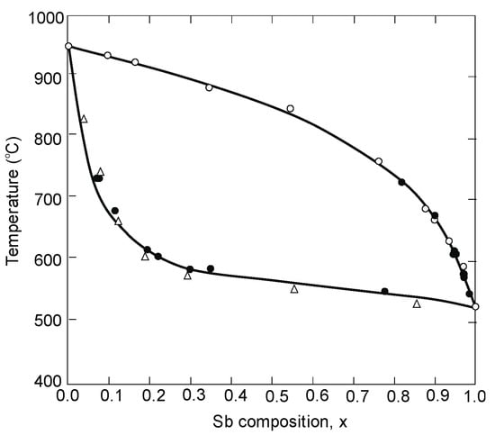
Figure 1.
Pseudobinary phase diagram for the InAs-InSb systems [1].
Progress in InAsSb ternary system has been limited by crystal synthesis problems. These difficulties are being overcome systematically by epitaxial methods such as: LPE, molecular beam epitaxy (MBE), and metalorganic chemical vapor deposition (MOCVD). Bulk single crystals are prepared mainly for compositions close to the binary compounds. A wide range of topics are gathered in thorough studies on electronic and photonic materials published in the Springer Handbook of Electronic and Photonic Materials [27].
LPE is a relatively simple high-quality technique, with less expensive epitaxial equipment and high utilization rate of the source material. It is particularly suitable for the preparation of thick-film layers. Since LPE technique is a near-thermodynamic equilibrium growth method, it cannot be used for the growth of the metastable ternary and quaternary antimonide compounds with miscibility gaps like InAsSb. The growth rate of LPE varies typically of 100 nm/min to a few μm/min (depending on substrate crystalline phases) and is generally higher than MBE and MOCVD. However, the controlled growth precision of very thin epilayers, especially quantum-well (QW) devices, SLs, and other complex microstructure materials cannot be implemented by LPE. In addition, the surface morphology of MBE or MOCVD grown layers is usually better than that grown by LPE.
The era of MBE and MOCVD growth of III–V semiconductors began in the early 1970s. It is often difficult to decide which epitaxial growth technique, MBE or MOCVD, to choose. Each of them has specific advantages in a given device application. Table 1 presents some characteristics related to the different classes of methods for III–V compounds [28].

Table 1.
MOCVD and MBE methods comparison (after [28]).
MBE heterostructures are grown in ultra-high vacuum (UHV) chambers (base pressure ~10−10 Torr) on heated substrates typically by elemental sources. The elements are directed from high temperature effusion cells toward the substrate in the form of streams being chemically unchanged. The temperature of the substrate is independently controlled to facilitate layer-by-layer material incorporation to the substrate. The use of carrier gas is not necessary-the inherently long mean free paths result in highly directional elemental beams and the UHV environment ensures high material purity. Fast shutters enable deposition of more sophisticated layer structures like SLs and QWs. The valved sources are generally used because of relatively high vapor pressures for V group elements. Gas sources (e.g., CBr4 for C doping), precursor sources (e.g., GaTe for Te doping), and plasma sources (e.g., nitrogen plasma) are applied.
MBE enables the control of the composition of the growing crystal with monolayer (ML) resolution due to the both slow growth rate (~1.0 ML per second) and mounting the shutters just in front of the crucibles. Calibration of the growing crystal with the electron beams is possible because of low background pressure in MBE. The layer-by-layer growth mode, III/V flux ratio, as well as the quality of the growing substrate can be determined by the reflection high energy electron diffraction (RHEED) technique. MBE provides the ability to control the interfaces by shutter sequence with a precision of 0.1 s because the growth proceeds in thermodynamic imbalance conditions. The leaks can be a major problem because the growth proceeds under extremely low pressure. The growth chamber is predominantly cooled by liquid nitrogen to strengthen high vacuum by preventing molecules from peeling off from the chamber walls.
MOCVD is another important growth technique widely used for heteroepitaxy of the QW structures and SL. Similarly to MBE, it also enables the growth of heterostructures with abrupt interfaces between the individual layers. The growth in MOCVD technique proceeds on a heated substrate but in a much higher pressure than MBE (typically 15 to 750 Torr). There are several types of MOCVD reactor designs. The growth proceeds at near atmospheric pressure in the atmospheric MOCVD and this requires the use of a large amount of carrier gases. In turn, the reactor pressure is kept low in the low pressure MOCVD and in this case the growth rate is then slower as in the MBE. Strict security precautions must be incorporated in the MOCVD laboratory. In order to avoid any deadly accidents, many safety precautions have to be implemented because the precursor gases and the carrier gases are often highly toxic or explosive. In almost all semiconductor fabrications, safety and environmental concerns are important issues because the growth processes are almost always associated with toxic and dangerous materials.
MOCVD growth proceeds not by physical deposition but by chemical reaction. In contrast to MBE, MOCVD technique requires more complex compound precursors, namely metal-organic sources (e.g., di-methyl or tri-ethyl Cd, Te, Al, etc.), hydrides (e.g., PH3, etc.), and other gas sources (e.g., Si2H6). The partial pressures of the precursors are controlled with mass flow controllers. In MOCVD, the precursors are transported over the substrate where they pyrolyze resulting in epitaxial growth. MOCVD requires the use of a carrier gas (typically hydrogen) to transport the precursors across the wafer surface. The valve actuation for varying injection ports of a gas manifold enables the growth of complex heterostructures. The fabrication of optoelectronics devices involving thermodynamically metastable alloys is dominated by both MBE and MOCVD techniques.
From the economical point of view (see Table 1 and [28]):
- the cost characteristics are very different because of the specific requirements:
- -
- for MBE the overhead is relatively fixed and does not vary with volume,
- -
- for MOCVD, the overhead costs tend to vary with production volume, and therefore
- MOCVD exceeds in a case of significant overcapacity (long idle time), and the opposite is true for MBE which wins on a cost basis when fully loaded,
- the two methods are very similar considering the production efficiency time,
- -
- for MBE, the idle time lasts on average several months where the reactor is down,
- -
- MOCVD service procedures are much more frequent but less time consuming, and therefore
- for MBE system, significant bake times are needed when the growth chamber must be opened for the service repairs,
- in contrast, MOCVD does not require long bake times (MOCVD is able to recover more quickly from failures).
Manasevit and Simpson firstly performed epitaxial growth of antimonides thin layers using MOCVD with TMGa (trimethylgallium) and SbH3 (stibine) precursors for GaSb films deposition in 1969 [29]. At present, the typically used III-group metal-organic sources by MOCVD for antimonide-based materials are 3-methyl compound and 3-ethyl compound, such as: TMAl, TMIn, TMGa, TEIn, TEGa, etc. [30,31]. In turn, V-group commonly used precursors are: AsH3, PH3, TMBi, TMSb, and RF-N2, etc.
The growth temperature of antimonides (low melting point materials) is close to 500 °C. It appears that below 500 °C the vast majority of III-group metal-organic precursors cannot decompose in 100%. Therefore, new organic source materials with a lower decomposition temperature are introduced including: TDMASb (trisdimethylaminoantimony), TASb (triallyantimony), TMAA (trimethylamine alane), TTBAl (tritertiarybutylaluminum), EDMAA (ethyldimethylaminealane), etc. In the case of Al-containing antimonide materials, carbon and oxygen contamination problems exist. The active hydrogen atoms’ absence on the surface of epitaxial layers is expected to be the reason of this effect. Carbon is typically p-type doping impurity, which causes certain difficulties in growing of n-type doping Al-containing antimonide epitaxial layers.
MBE grown antimonides was first reported in the late 1970s [32,33]. In comparison with GaAs and other arsenides, the growth of GaSb-based is characterized by relatively low Sb vapor pressures, or, equivalently, by its high sublimation energy. GaSb and AlSb are nearly lattice-matched mutually and to InAs and for this reason they are the subject of intensive research. The substrate temperature during the growth of GaSb and AlSb is usually between 550 and 600 °C. MBE reduces the concentration of O-doping and avoids the C-contamination issue in Al-based materials growing by MOCVD. Most of low-dimensional structures (quantum wires-QRs, QWs, and quantum dots-QDs) and devices having complex structures were first grown by MBE. It was experimentally proven that the implementation of crystallographically misoriented substrates (small angle offset) contributed to higher-quality epitaxial layers [34].
The growth of antimonide-based III–V epitaxial layers is usually performed on InSb, InAs, and GaSb low-defect substrates. GaAs and GaAs-coated Si substrates and other heterogeneous substrate materials for epitaxy were introduced to face the problem that antimonides have no semi-insulating substrate. The growth of multilayers with abrupt but incremental compositional shifts between adjacent layers and continuous compositional grading of thick epilayers enables one to obtain a variety of substrate structures. Wafer bonding techniques and selective removal of the seeding substrate methods can be combined in IR detector fabrications. With high-quality substrates with increased functionality and bandgaps and lattice constants differing significantly more than feasible with binary compound wafers (e.g., GaSb or InAs), it seems possible to implement [35].
The initial efforts in fabrication and characterization of InAsSb material until 1994 were described in two Rogalski papers [19,21]. The book chapter written recently by Steenbergen [20] has provided updated information on the growth methods and characterization techniques of InAsSb bulk and SLs materials for the last thirty years. Because of this, here only main trends in material fabrication are covered.
Current interest is directed toward the InAsSb photodetectors cut-off wavelength (λcut-off) extension beyond that available when lattice-matched or lattice-strained to binary substrates; mainly GaSb. In order to improve FPAs manufacturability and increase their size, low-cost GaAs and Si substrates are used. The Si substrates are very convenient in IR FPA technology because the coupling with Si readout enables fabrication of very large arrays exhibiting the prolonged thermal cycle reliability (Si substrates are cheaper and available in large area).
In practical design of InAsSb-based device structures, a serious problem is the control of photodetector’s λcut-off. The accuracy of the bandgap depends on material composition, stress in the buffer layer between substrate and the active region, the crystalline quality of the ternary samples, (potentially CuPt ordering) which is determined by the growth method and conditions, and finally the bandgap measurement uncertainty. Different techniques used in bandgap characterization (absorption, ellipsometry, photoluminescence (PL) and electroluminescence (EL)) and experimental results are given by Steenbergen [20].
Usually, the spontaneous ordering of CuPt in mid-composition range of InAs1−xSbx causes a problem. Better alloy composition uniformity of group V materials on lattice-mismatched substrates is required to grow controlled, high crystalline quality InAsSb without spontaneous ordering [36]. In the technology of ternary semiconductors, atoms of group V having different sticking coefficients are more difficult to control than group III ternaries [37,38]. Using modulated MBE (MMBE) technique with arsenic and antimony shutter modulation (see Figure 2), better control of InAsSb composition is reached.

Figure 2.
The scheme of the MMBE shutter sequence during the growth of InAs0.76Sb0.24 and the surrounding InAs layers. The filled bars denote intervals when the corresponding shutters are open (after [37]).
The spontaneous CuPt ordering during InAsSb MBE growth is probably caused by residual strains [39]. Figure 3 presents the crystal structure of CuPt-ordered InAs0.50Sb0.50 and the calculated band structure indicating inversion of the Λ4,5 and Λ6 bands, pointing the semimetallic character.
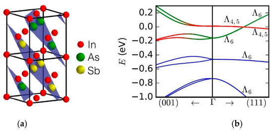
Figure 3.
CuPt-ordered InAs0.50Sb0.50: (a) crystal structure with the alternating Sb-As (111) planes highlighted, (b) empirical tight binding band structure calculation around Γ for |k| ≤ 0.1 Å−1 (after [40]).
The quality of InAsSb has improved greatly in the last decade. Significant progress has been made to advance metamorphic buffer layers for LWIR MBE photodetector structures. Different compositionally graded buffer schemes have been studied with the absorber composition x ≈ 0.60, including GaInSb and AlGaInSb graded buffer layers on a GaSb substrate to extend detector’s λcut-off [41,42].
In comparison with MBE, MOCVD also allows to grow epitaxial structures on large-area wafers providing higher production throughput (MOCVD is more economical and characterized by less problematical maintenance). However, a disadvantage of this technique is less sharp interfaces, especially in SLs fabrication. More details about InAsSb structures MOCVD growth are included in [20].
3. InAsSb Alloy Properties
Table 2 shows selected properties of semiconductors, along with narrow-gap alloys, used in IR photodetectors manufacturing characterized by zincblende (ZB) or diamond (D) crystal structure. There is a tendency in transition of chemical bond from the covalent group IV-semiconductors to more ionic II–VI materials with the lattice constant increasing when moving across the table from the left to the right. The materials become softer and the chemical bonds become more delicate which results in the quality of the bulk. The semiconductors with a greater share of covalent bonds are more mechanically stable, which contributes to better fabrication. The supreme position of GaAs in optoelectronics and silicon in electronic materials supports this observation. In turn, the energy gap of semiconductors on the right side of the table shows a tendency to have lower values. Higher band-to-band (BtB) absorption provides increased quantum efficiency (QE, η) observed for example in HgCdTe or InSb because of their direct bandgap structure.
Table 2.
Fundamental properties of semiconductors used in IR photodetectors manufacturing.
A high density of states in the valence band (VB) and conduction band (CB) leading to enhanced absorption of IR radiation and a comparatively low thermal generation rate arise from the direct energy bandgap structure of narrow gap semiconductors applied in the IR detectors. The III–V semiconductors are characterized by much stronger chemical bonds and therefore higher chemical stability compared to HgCdTe, which is important from the producibility viewpoint.
3.1. Energy Gap
The III–V semiconductors are characterized by a ZB structure and direct energy gap at the Brillouin zone centre. The k · p theory explains the shape of the electron and the light mass hole bands. For different semiconductors, the momentum matrix element changes slightly and is typically about 9.0 × 10⁻⁸ eVcm. Therefore, the CB densities of states and the electron effective masses have comparable values for materials with the same energy gap.
The Varshni formula clearly describes a conventional negative temperature coefficient of the energy gap of these materials [43]:
where Eo is the bandgap at 0 K, T is the temperature, α and β are fitting parameters for a given material. β is closely related to the material’s Debye temperature (in Kelvin).
If T >> β, then Equation (1) becomes ∂Eg(T)/∂T ~−α. Viña et al. [44] proposed a new expression for temperature dependence of the bandgap energy by taking into account the Bose–Einstein occupation factor [45]
where the parameter describes the mean frequency of the phonons involved and αB is the strength of the electron-phonon interaction. While Varshni expression is entirely empirical, the Bose–Einstein retains physical meaning and is more palatable from the theoretical point of view. It is assumed that the Varshni parameter β is comparable to the Debye temperature, Θ = <Ep>/k, thus the Bose–Einstein average phonon energy can be used to calculate the Debye temperature. If kT >> <Ep>, the Varshni and Bose–Einstein expressions are equivalent. For lower temperatures in which kT < <Ep>, the Bose–Einstein formula usually provides a better fit to the experimental results (Ref. [20] discusses in detail the bandgap temperature-dependent parameters).
The dependence Eg(x,T) for InAs1−xSbx has been experimentally investigated by many research groups since 1964 [22]. The first investigation of the polycrystalline samples optical properties indicated on the nonlinearity of the InAs1−xSbx bandgap composition dependence, which can be represented by the bowing parameter Cg as
Ten different relations Eg(x,T) obtained from measurements over different x-composition values for a wide range of temperatures are presented in [20]. The low-temperature (4–13 K) λcut-off estimated from λcut-off [μm] = 1.24/Eg[eV] changes from 8.4 μm to 12.5 μm. The smallest bandgap of InAs1-xSbx occurs for x ≈ 0.60–0.64; however, for such composition lattice-matched binary substrate has not been developed yet. The bandgap expressions from many papers are plotted in Figure 4 and Figure 5 for both high and low temperatures.

Figure 4.
InAs1−xSbx bandgap energy versus the Sb composition at room temperature. The experimental data is taken with different papers [46,47,48,49] as indicated in the legend.
At present, Cg value close to 0.7 eV is correct in higher temperature range (Figure 4). The evaluated Eg(x,T) dependence differs from that previously described by Wieder and Clawson in 1973 [46]:
Initial reports based on experimental data at temperatures above or near 100 K estimate the direct-gap bowing parameter in InAsSb at 0.58–0.6 eV [50]. According to Rogalski and Jóźwikowski’s theoretical considerations, the bowing parameter should tend to move to a higher value of about 0.7 eV [51].
The experimental data from VIGO System collected in recently published paper [47] fits well with a parabola having C = 0.72 eV and relation
This relation is recommended for InAsSb layers grown on GaAs lattice-mismatched substrates and is valid for both low and high temperatures.
More recent PL studies on unrelaxed MBE-grown InAs1−xSbx in wide range of composition gave the bowing parameter from 0.83 to 0.938 eV [39,42,49,52]. Until now, the highest bandgap bowing parameter 0.938 eV for low temperature has been reported by Webster et al. [49]. Such large parameter results in the considerable reduction in the smallest bandgap, ≈25–75 meV, at low temperature. At room temperature, Webster et al. [49] have obtained much lower bowing parameter of 0.75 eV and developed the temperature-dependent bandgap bowing model. The literature data for InAsSb layers grown by MBE on GaSb fits well with this model end equation
Figure 5 summarizes the experimental data and theoretical predictions of energy gap in temperature range 4–77 K published in different papers. Discrepancies in the Eg(x,T)-dependence may result from several factors among others: strains, structural quality of samples, and CuPt-type ordering effect.

Figure 5.
InAs1−xSbx bandgap energy versus the Sb composition at low temperatures. The experimental data are taken with different papers as indicated in the key [39,41,42,49,52,53,54,55,56].
The low energy gap data reported earlier were masked probably by electron filling of the CB, which resulted from background doping due to various degrees of residual strain and relaxation in these samples. As is marked in Section 2, high quality of unstrained and unrelaxed InAsSb epilayers have been developed by using special graded buffer layers which reduces the substantial difference between the lattice constant of the alloy and the substrate. Electron diffraction patterns of unstrained InAsSb alloys, described in [41,42], showed an ordering-free distribution of group V elements, which indicates that the observed energy gaps of ternary alloys are inherent (both ordering and residual strain effects were eliminated).
The above discussion indicates that the InAsSb bandgap energy is approximately a square function of the composition and shows a weak dependence of the band edge on composition in comparison with HgCdTe (see Figure 6).

Figure 6.
Composition and wavelength diagram of semiconductor material systems.
3.2. Bandgap Alignment and Offsets
The SL photodetector’s design process requires the bandgap alignment and offsets for InAsSb in relation to InAs, InSb, and other III–V semiconductor alloys. As is shown in Figure 6, these materials belong to 6.1 Å III–V semiconductor family. They are the most important in proposing new solutions of high-performance IR detectors exhibiting direct energy gaps, high optical absorption, and high design flexibility. This group consists of three alloys having approximately matched lattice constant about 6.1 Å: InAs, GaSb, and AlSb. Their energy gaps are varying in the range starting from 0.417 eV (InAs) to 1.696 eV (AlSb) at lower temperatures [57]. Similarly to other semiconductor compounds, they are chosen as the subject of research due to their heterostructures, in particular combining InAs with the three antimonides (InSb, AlSb, and GaSb) and their alloys. This combination provides a band alignment that is fundamentally different from that of the more thoroughly researched AlGaAs and that band alignment flexibility draws the attention of scientists on the 6.1 Å materials. InAs/GaSb heterojunctions reveal the most unique band alignment, which is defined as the broken gap. The top of the VB of GaSb is located above the bottom of CB of InAs by ~150 meV at the interface. On both sides of the heterointerface, electrons and holes are separated and located in self-consistent QWs, which is related to partial overlapping of the InAs CB with the GaSb VB. Consequently, exceptional tunneling-assisted radiative recombination transitions and novel transport properties are observed. A wide range of different alloys and SLs can be designed due to high versatility of these compounds, with the accessibility of type-I (nested, or straddling), type-II staggered, and type-II broken gap (misaligned) band offsets between the GaSb/AlSb, InAs/AlSb, and InAs/GaSb material pairs, respectively, as illustrated in Figure 7.

Figure 7.
Schematic diagram of the low-temperature energy band alignment in the nearly 6.1 Å lattice matched InAs/GaSb/AlSb compounds. In this material system three types of band alignment are possible: type-I (nested) band alignment between GaSb and AlSb, type-II staggered alignment between InAs and AlSb, and type-II misaligned (or broken gap) alignment between InAs and GaSb. The approximate values of band offsets are marked in red.
Due to different growth conditions causing the variety of residual strain in the materials and due to the discrepancies related to the bandgap measurement methods, the band offsets are historically not easy to estimate. Steenbergen et al. [58] have reviewed the band edge alignment models for InAs-InAs1−xSbx system and considered different types of heterojunctions. This review is updated in recently published monograph [20]. Figure 8 shows three possible band alignments between InAs and InAs1−xSbx including two type-II band alignments: with the InAs CB higher in energy than the InAsSb CB and with the InAsSb CB higher in energy than the InAs CB. From these two papers [20,58], the following conclusions could be drawn:

Figure 8.
Three possible band alignments between InAs and InAs1−xSbx.
- the type-I alignment is notified for SLs with low Sb compositions and ordering typical for the InAs1-xSbx layer, which is characterized by a lower alloy bandgap than that of a random alloy with equal composition x [59],
- the type-IIa alignment is based on argued conclusions for the reduced mass values of the lowest two transitions given by PL and magneto-transmission measurement results [60,61],
- type-IIb, is chosen for InAs/InAs0.93Sb0.07 SLs on InAs substrates [62].
Investigations carried out during the last several years have revealed the InAsSb band edges versus composition dependence as shown in Figure 9 [20]. The recommended parameters are as follows: InAs/InSb valence band offset (VBO), −0.59 eV; the InAsSb bandgap bowing, 0.87 eV; and the VB bowing, –0.35 eV. Moreover, a concept of the band offsets between InAs and InAsSb with slight dependence on temperature was introduced. It follows that the bandgaps are the main temperature-dependent factors with the band offsets and VB bowing being distributed by the same fractions in the whole temperature range [49].

Figure 9.
InAs1−xSbx VB and CB edges and their alignment assuming that x = 0 for InAs and x = 1 for InSb. As noted by the dashed arrow, longer wavelengths than InAsSb can be reached with T2SLs grown on a virtual substrate InA0.54Sb0.46 (after [20,63]). Bandgap bowing, Cg, has been distributed to the VB, Cv, and CB as shown according to the references [49,64]. The dash-dot curves represent the suggested bandgap and VB bowing equal 0.87 and −0.35 eV, respectively. The solid arrow points the composition of InA0.91Sb0.09 lattice-matched to GaSb substrates.
The InAsSb properties are direct consequence of the energy band structure. Table 3 contains some material parameters of the InAs, InSb, GaSb, and InAs0.35Sb0.65 semiconductors [3,65]. Between them, InSb has been investigated most broadly.
Table 3.
Physical properties of narrow gap III–V alloys.
3.3. Transport Properties
Virtual crystal approximation (VCA) describes the electronic properties of ternary alloys according to the approach [66], where the disordered alloy is modeled by an ideal crystal with an average potential at each sublattice site. Linear interpolation of the potentials of corresponding binary semiconductors is realized by the potential averaging. The nonlinearity of composition dependence versus the energy gap (see Equation (3)) is calculated based on VCA model because of the nonlinear relationship of the band energies against the crystal potential. In order to explain the large bandgap bowing, the VCA has to be modified by adding the random potential due to fluctuations of the alloy composition [67,68]. Presently, it is commonly assumed that the material disorder influences not only the large bandgap bowing in the InAsSb alloy but also shapes the composition dependence on fundamental parameters such as mobilities or carrier effective masses.
The conduction-valence-band mixing theory [23] has been implemented to obtain a good agreement between experimental room temperature effective masses and calculations, as reported by Rogalski and Jóźwikowski [51] (see Figure 10). More recently published low-temperature data, especially for mid-composition range, indicates lower electron effective masses. Estimated negative bowing parameter for the electron effective mass is Cm = 0.038 and is slightly less than expected from the Kane model (Cm = 0.045), reaching the lowest effective mass (0.0082m0 at x = 0.63 and 4 K) ever reported for III–V semiconductors. A possible reason for the effective mass value discrepancy, shown in Figure 10, is the alloy disorder causing the random potential distribution which disturbs the CB and VB states.

Figure 10.
Effective mass of electron versus composition for InAs1−xSbx. The experimental data is taken from [51,56].
The electrical properties of semiconductor compounds and their dependence on composition are very important for device design with the optimal performance. However, it is difficult to control carrier concentration because insulating or semi-insulating substrates for InAsSb epitaxial layers are generally not available. Parallel conduction layers such as the substrate and/or the interface with the substrate presence make Hall effect measurements difficult to interpret. Moreover, it has been well known from the beginning of the 1970s [69,70] that narrow gap III–V semiconductors, especially InAs, creates surface electron accumulation layers. For example, Figure 11 presents band edges of p-type InAs [69] and InAsSb [71] with surface electron accumulation. There is strong electron accumulation on the InAsSb side of InAsSb/GaSb heterojunction due to the staggered type II band alignment. As is shown in Figure 11b, the surface states cause the Femi level to be pinned above the CB creating a parallel conduction path to the epilayer. In this case, the accurate determination of the carrier concentration and mobility with standard Hall measurements is challenging.
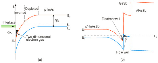
Figure 11.
Band edges of p-type InAs and InAsSb with surface electron accumulation: (a) InAs with surface inversion layer; the electrostatic potential has the value Φs at surface and Φb in the bulk, (b) InAsSb/AlAsSb heterojunction with depicting surface electrons, epilayer, and interface with AlAsSb.
The above-mentioned effect should be taken into account to analyze electrical carrier concentration and mobility measurements. A popular two-layer model has been often used to separate the surface accumulation and epilayer properties. Another approach is applied in the case of more complicated structures like that shown in Figure 11b. Mobility spectrum analysis and/or variable temperature and magnetic field-dependent transport analysis with multicarrier fitting models have been applied to segregate the epilayer and surface and interface layer characteristics [71].
The variation of InAs1–xSbx electrical properties depend on the composition. Similarly to binary compounds, ternary alloys also have the surface accumulation layers and interface layers with the buffers or substrates. Special attention is required in estimates of carrier concentrations in selected device regions. More information on that topic can be found in [20].
As a popular donor dopant in InAs, silicon is used. Beryllium and zinc have been used for InAs and InSb photodiode fabrications for conversion of n-type materials to p-type ones [3]. Silicon behavior in InSb is amphoteric; in pulled crystals results in p-type conductivity for temperatures >400 °C, however for MBE growth epilayers results in n-type when the growth temperature is >350 °C, but for growth temperatures <320 °C gives donor conductivity [20]. Germanium is used as an acceptor dopant in InSb but behaves as a donor in InAs for LPE-grown epilayers [72].
Rogalski and Jóźwikowski have calculated the InAs1−xSbx intrinsic carrier concentration for the conditions 0 ≤ x ≤ 1 and 50 ≤ T ≤ 300 K. In order to obtain a good agreement between experimental values and calculations, the conduction-valence-band mixing was taken into account [51]:
where ni is in cm−3 and k is the Boltzmann constant. The maximum of ni occurs at x ≈ 0.63 which corresponds to the minimum energy gap for a given temperature.
The CB density of states is low due to the very small effective mass of electrons and filling the available band states can be realized by doping shifting the absorption edge to shorter wavelengths. This phenomenon has been recognized as the Burstein-Moss (BM) effect, which is shown in Figure 12 for n-type InAs0.855Sb0.145 epilayer with residual background donor concentration of 3 × 1016 cm−3.

Figure 12.
PL (a) and absorbance (b) spectra of 5-µm thick InAs0.855Sb0.145 MBE epilayer deposited on GaAs substrate with 3-µm thick InAs buffer layer. The residual background donor concentration is 3 × 1016 cm−3 (after [47]).
The theoretically predicted absorption was calculated using the Kane model, including the BM shift according to Anderson theory [73]. As is shown, the experimental spectrum is in proper agreement with the theoretical absorption simulation at 20 K and 300 K. The bandgap energy values measured with IR transmission spectroscopy agree with those obtained from PL peaks, particularly at low temperatures.
The first measurements of transport properties of n-type InAsSb alloys were performed on samples prepared in the late 1960s by various freezing and annealing techniques [74,75]. The properties of high-quality InAsSb epitaxial layers with x < 0.35 fabricated by LPE are comparable to those of pure InAs (when n = 2 × 1016 cm−3, typical mobilities are 30.000 cm2/Vs at 300 K and 50.000 cm2/Vs at 77 K). For InSb-rich alloys with x ≥ 0.90, typical mobilities are 60.000 cm2/Vs at 300 K. When As is added to InAs1−xSbx alloys, the residual background concentration has increased to a low 1017 cm−3; in turn the mobility first increased and then dropped by a factor of 1.5 to 2 as the temperature decreases from 300 to 77 K. At the present stage of MBE-growth development, the background electron concentration in InAs1–xSbx with 40% Sb at 77 K is as low as 1.5 × 1015 cm−3 [39].
The carrier mobility in the III–V binary compounds is primarily limited by scattering due to optical phonons, and ionized impurities with a contribution from alloy disorder in the corresponding ternary alloy. The last kind of scattering mechanism is so-called alloy scattering. Their relative contributions depend on temperature, carrier concentration, compensation, and alloy composition. Acoustic phonon and deformation potential, optical deformation potential, and neutral impurity scattering are minor effects under most conditions. The total carrier mobility μtot in alloy InAs1–xSbx can be simply expressed as [27]:
The first two terms of Equation (8) result from the linear interpolation scheme and the third term reflects the effects of alloying.
The InAs1−xSbx mobility composition dependence is illustrated in Figure 13 at 77 and 300 K for carrier concentrations of experimental significance [76,77]. The component mobilities are shown for carrier concentrations of n = 1015, 1016 and 1017 cm−3 at 77 K, and 1016, 1017 cm−3 at 300 K. A decrease in impurity concentration causes continuous increase of carrier mobility throughout the temperature range. The significance of alloy scattering is visible when temperature and carrier concentration decrease as the respective contributions from polar optical phonons and ionized impurities are reduced, until it remains as the dominant scatterer across most of the compositional range for low carrier concentrations (below 1015 cm−3) and low temperatures.

Figure 13.
InAs1−xSbx mobility composition dependence at 77 K. The solid lines are the calculated mobilities for selected carrier concentrations, and the dashed lines are the component mobilities determined for a carrier concentration of 1015 cm−3 [77]. Experimental data is marked for epitaxial layers with carrier concentrations between 1015 to 1016 cm−3. Scattering legend: µop-optical phonons, µi-ionized impurity, µalloy-alloy disorder.
Egan et al. have calculated the electron mobility of InAsSb by considering all the possible scattering mechanisms: impurities, acoustic phonons, optical phonons, alloy scattering, and dislocations [77]. Comparison with experiment confirms that dislocation scattering has a strong effect on transport, while alloy scattering limits mobility in ternary samples grown with a minimum of defects (see Figure 14).

Figure 14.
InAs1−xSbx electron mobility composition dependence for room-temperature (solid lines [77]) and carrier concentration of 1017 cm−3 with a compensation ratio of 0.2 and the effects of a dislocation density of 3.8 × 108 cm−3. The experimental data is taken after [20,23] for samples with electron concentrations above 1016 cm−3.
The next figure (Figure 15) presents the modeled InAs0.80Sb0.20 electron and hole mobilities temperature dependence with low residual background doping [78]. As is shown, the mobility ratio b = μe/μh assumes ~102, similarly to InSb.

Figure 15.
Modeled mobility versus temperature for electrons and holes in undoped InAs0.80Sb0.20.
3.4. Thermal Generation-Recombination Processes
The photodetector’s performance depends directly on the generation-recombination (G-R) processes, determining a steady-state concentration of carriers in semiconductors based on the optical (kinetics of photogenerated carriers) and thermal excitation. A wide study of G-R processes in semiconductors is reported in literature (see for example [79,80,81]). We describe here only selected carrier lifetime results directly related to photodetector performance. Assuming bulk processes only, there are three main thermal G-R processes to be considered in the narrow bandgap semiconductors: SRH, radiative, and Auger.
The statistical theory for the G-R processes via intermediate centers was developed first by Shockley and Read [82], and Hall [83]. It may be reduced by decreasing foreign impurities and native defects concentrations, which can be achieved by low-temperature growth and by progress in the material’s development. Since the SRH does not represent a fundamental limit to photodetector performance (it can be reduced with progress toward purer and higher-quality material), a significant research effort is still needed.
Absorption of internally generated photons causes the radiative generation of charge carriers. The annihilation of electron-hole pairs with emission of photons makes an inversed process. Internal radiative processes are the fundamental factor limiting the detector performance. However, critical re-examination of the radiative mechanism contribution in the IR detection has been presented in the literature [84,85]. Humpreys [84] indicated that due to photon reabsorption (PR), the radiative lifetime is highly extended and depends on the semiconductor geometry. Under reverse bias operation where the electron density in the active layer is reduced below its equilibrium level, the internal radiative generation could be suppressed [86]. In spite of the fundamental nature, the radiative processes do not limit significantly the ultimate performance of IR detectors, especially in the LWIR range [87].
In high-quality narrow gap semiconductors such as InSb and Hg1−xCdxTe, Auger mechanisms determine G-R processes at near room temperatures. The Auger mechanisms in InSb-like band structure materials are classified into 10 photonless mechanisms according to the related bands. Figure 16 presents the three predominant mechanisms in the case of this type of band structure. They are characterized by the largest combined density of states and smallest threshold (ET ≈ Eg).

Figure 16.
The three BtB Auger recombination processes. Arrows indicate electron transitions; •, occupied state; ○, unoccupied state.
The conduction band/heavy-hole band/conduction band (CHCC) recombination mechanism (also labeled Auger 1) prevails in n-type material and involves two electrons and a heavy hole. For p-type material the conduction band/heavy-hole band/light-hole band (CHLH) process (marked as Auger 7) is characteristic under condition that the spin split-off band can be neglected. Auger transition probability through the conduction band/heavy-hole band/spin split-off band mechanism (labeled CHSH or Auger S hereafter) can be ignored for semiconductors such as InSb and HgCdTe where the spin split-off energy (∆) is much larger than the bandgap energy Eg and the Auger 7 transition is typical.
The spin split-off band is even more essential than the light-hole band for the direct-bandgap materials, particularly when the bandgap energy Eg approaches the spin-orbit splitting ∆ (as in the case of InAs and InAsSb). The carrier lifetimes in binary compounds (InSb and InAs) are discussed in detail in chapter 2 monograph Antimonide-Based Infrared Detectors. A New Perspective [88].
Figure 17 summarizes the InAs1−xSbx spin-orbit-splitting energy, ∆, composition dependence at 10 K. Experimental results of ∆(x) dependence published in 1972 by Van Vechten et al. [75] differ more strongly than that presented recently in the paper by Cripps et al. [89]. The ∆ parameter versus x (Sb fraction) characteristic does not show bowing clearly. A good approximation can be calculated with

Figure 17.
InAs1−xSbx spin-orbit-splitting energy versus composition at T = 10 K. The dotted straight line represents the zero bowing behavior consistent with the VCA. The single points represent experimental data [75,89].
The above formula allows for the calculation of the spin-orbit-splitting bandgap energy which stays in a good agreement with experimental results and does not depend on temperature.
For slight deviation from equilibrium and for nondegenerate materials with equilibrium carrier concentration no (or po), the carrier lifetimes can be calculated using the intrinsic carrier lifetime and no/ni (or po/ni) ratio [65,79]:
for radiative recombination:
for Auger recombination:
The InAs1−xSbx Auger and radiative recombination carrier lifetime for the composition range 0 ≤ x ≤ 1 and the temperature range 77–300 K was estimated by Rogalski and Orman [90]. Radiative recombination determines the carrier lifetime in the low temperature range. At higher temperature, the Auger 1 process is dominant in n-type InAs1–xSbx but in p-type material, for the composition range 0 ≤ x ≤ 0.3, Auger 7 and Auger S processes compete while for x > 0.3, the Auger 7 process dominates. Different recombination mechanisms in InAs0.35Sb0.65, operating at the longest λcut-off, (with Eg close to 0.1 eV at room temperature) are also discussed in [90].
The dependence of , and on the composition x in InAs1–xSbx at room temperature is presented in Figure 18. The effect of the Auger S process was considered as accurate for 0 ≤ x ≤ 0.3 according to the out-of-date carrier lifetime calculation [90]. The predicted contribution of Auger S process is dominant in InAs1−xSbx semiconductors close to InAs (for 0 ≤ x ≤ 0.15) taking more recently estimated dependence of ∆(x) [89]. It follows that InAsSb photodiodes have lower Auger S nonradiative losses than were reported previously [91]. This adjustment has substantial implications on the p-type InAsSb-based devices’ design.
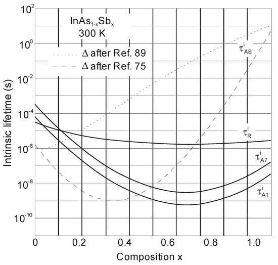
Figure 18.
Intrinsic InAs1−xSbx Auger and radiative recombination carrier lifetimes at room temperature. is calculated assuming spin-orbit-splitting bandgap energies after [75,89] (after [91]).
Generally, in III–V semiconductors the carrier lifetime is not limited by the BtB recombination but by SRH mechanism. Two regions are of interest:
- the neutral or diffusion region of the detector, and
- the depletion region of the detector.
As discussed in many papers, there are two types of possible SRH defects-neutral centers at the intrinsic level with carrier lifetimes τpo ~ τno and charged centers at some specific energy level in which there is a large asymmetry in the lifetimes associated with electrons and holes.
In comparison with II–VI HgCdTe, the reported SRH lifetimes in the majority of III–V binary alloys are not impressive. For example, the best values for InSb indicate that τSRH is about 400 ns for LPE-grown material [92]. It is interesting to stress that this value has not been improved over the last 60 years, and no response defect has been identified. Similar lifetime was reported for MBE grown InAs/InAs0.72Sb0.28 T2SLs. Assuming this carrier lifetime value, Kinch modeled the minority carrier lifetime and diffusion length versus temperature for holes in n-type InAs0.81Sb0.19 with doping levels 1015 and 1016 cm−3-see Figure 19 [78]. These values are approximately three orders of magnitude smaller than those in HgCdTe with similar bandgaps.

Figure 19.
Simulated minority carrier lifetime and diffusion length versus temperature for holes in n-type InAs0.81Sb0.19 with doping levels 1015 and 1016 cm−3 and τSRH = 400 ns.
3.5. Other Properties
The optical properties of InAsSb are determined by a nonparabolic three-band model. Dobbelaere et al. [93] have studied IR absorption spectra of Si-doped MBE epitaxial layers grown on Si and GaAs substrates. The absorption coefficient was measured in the wavelength range 3–12 μm and the experimental data were fit by an analytical formula that was derived from the Kane band model. Excellent agreement between the calculations and the measurements was observed (Figure 20). Due to the fact that the measurements were carried out for InAs1−xSbx with x ≈ 0.70, a large shift of the absorption edge with Si doping was observed due to low density of states in the CB. This has been referred to the BM effect.

Figure 20.
Absorption spectra for InAs0.30Sb0.70 grown on GaAs substrates at 300 and 77 K with electron concentrations (a) 1017 cm−3 and (b) 2 × 1018 cm−3. Solid lines present theoretical fitting (after [93]).
Comparable values of absorption coefficients for bulk HgCdTe [94,95] and InAsSb [49,96] are reported (see Figure 21), proving relatively minor differences between densities of states in bulk semiconductors with the same energy gap and the optical matrix elements.

Figure 21.
Intrinsic absorption coefficient for Hg1−xCdxTe, InSb, and lattice-matched InAs0.911Sb0.09 and InAs/InAsSb SLs at room temperature.
The Raman spectroscopy is a well-known technique to understand the lattice vibrations of various material systems. The first Raman spectroscopy study of InAs1−xSbx on InAs and InSb substrates was performed by Cherng et al. [97]. They reported “one-mode” phonon behavior for x ≤ 0.6 and “two-mode” phonon behavior for larger values. Then, a similar study for InAsSb grown with different composition on GaAs substrate by MBE was carried out in [98,99], and “two-mode” phonon behavior was observed. Along with the Sb composition increasing in InAs-like longitudinal-optical (LO), transverse-optical (TO) phonon peaks reveal a blue and red-shift occuring for InSb-like LO phonon peak-see Figure 22. Recently, Grodecki et al. [100] suggested that spectra in the region 20–160 cm−1 are caused by zone folding in phonon dispersion curves as a result of CuPt unit cell of InAsSb being twice as large as typical ZB unit cell.
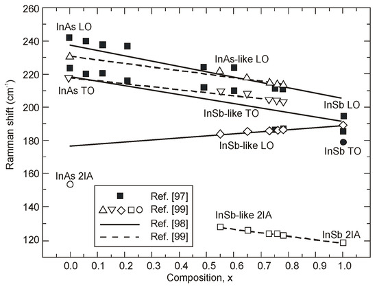
Figure 22.
InAs1−xSbx Raman frequency dependence versus composition (after [99]).
4. Properties of InAs/InAsSb Superlattices
Ting et al. published simple theoretical considerations on the fundamental T2SLs parameters [101]. Their properties differ strongly from those of constituent layers.
InAs/InAsSb SLs have been less researched than InAs/GaSb SL and they are in the early stage of development. Because of only two common elements (In and As) in SL layers and rather uncomplicated interface structure with Sb-shifting elements, the InAs/InAsSb SLs growth follows with a better controllability and easier manufacturability. It appears that InAs/InAsSb SLs are more flexible in the optimization of device performance. In order to reduce the tension between the SL layers and the substrate on which the SL is deposited, a suitable selection of the buffer layer is required in which the tension between the SL and the buffer layer is averaged. Usually, in order to fabricate the defect-free buffer layer, the interfacial misfit array (IMF) technique is applied [102]. By producing the strain-balanced SL to the buffer layer, the influence of the strains and dislocations on the device performance is eliminated.
The carrier localization effect is noticed in T2SLs at low temperature because of local impurities and spatial variations in the CB and VB potentials, layer thickness variation, or composition variation. These local potentials result in low-energy tail states (lower than the bandgap), which can trap carriers. The presence of carrier localization is supported by observation of extremely long carrier lifetimes and PL peak blue shifts at low temperatures [20,103]. The InAs/InAsSb interface disorder was found to be the reason for the carrier localization [104]. Therefore, the greater effect from interface disorder and deeper localization potentials are observed in smaller SL periods. The carrier localization effects are not observed at higher temperatures (>100 K).
4.1. Bandgap Energy and Effective Masses
Since InAs is not lattice-matched to InAsSb, the changing of the layer thickness requires a good understanding of the strain contribution on the material quality. Figure 23 shows the SLs InAs/InAs0.62Sb0.38 band structure for unstrained and strained conditions. Under the influence of strain, an electron affinity changes and the VB splits on the heavy and light holes’ sub-bands.
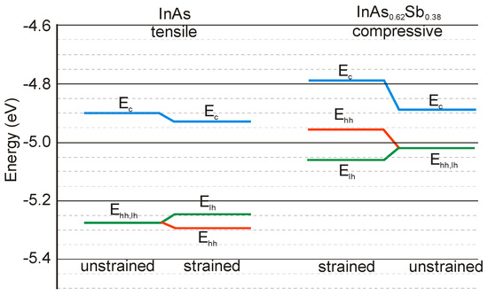
Figure 23.
The energy band profiles of unstrained and strained InAs/InAs0.62Sb0.38 SLs (after [105]).
The basic difference in profiles of the CB and VB in the InAs/GaSb and InAs/InAsSb T2SLs is presented in Figure 24. The band alignment of T2SL is causing a state in which the energy bandgap of the SLs can be adjusted to the configuration, either a semimetal or a narrow bandgap semiconductor material.
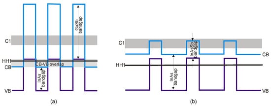
Figure 24.
Bandgap diagram for (a) InAs/GaSb and (b) InAs/InAsSb T2SLs (after [106]).
Transitions between electron and hole bands are spatially indirect. The first electron miniband (C1) is more sensitive to layer thickness than first heavy hole state (HH1) because of the large value of the heavy-hole mass.
Below are emphasized distinctions in the fundamental properties of InAs/GaSb and InAs/InAsSb SLs:
- both type of T2SLs are based on nearly-lattice-matched III-V semiconductors and provide a large range of tunability in λcut-off,
- in T2SLs the electron and hole wave functions are located in separate layers,
- the resulting energy gap is determined by the transition energy between the HH1 and the C1 and depends upon the layer thicknesses and interface compositions,
- the band offsets in conduction (∆Ec) and valence (∆Ev) bands in the InAs/InAsSb SL (∆Ec ~142 meV, ∆Ev ~226 meV) are much smaller as compared to InAs/GaSb SL (∆Ec ~930 meV, ∆Ev ~510 meV),
- a much larger broken gap of the InAs/GaSb SLs makes it easier to reach small SL bandgaps,
- as the period increases, the λcut-off of the InAs/GaSb SL increases much faster than in the case of the InAs/InAsSb SL. Shorter period of InAs/GaSb SL gives the same λcut-off as for InAs/InAsSb SL.
Figure 25 shows the theoretically estimated the λcut-off versus SL period for strain balanced (with respect to the GaSb substrate) InAs/GaSb and InAs/InAsSb T2SLs. In order to achieve strain balance between InAs/GaSb SLs layers, InAsSb interfacial MLs are inserted between the InAs and GaSb layers. As is shown in Figure 25, the (m,n)A/B denotation means SLs with MLs of material “A” and MLs of material “B” in each period of (m + n) MLs.
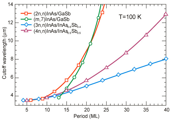
Figure 25.
Theoretically estimated λcut-off for (2n,n)InAs/GaSb, (m,7)InAs/GaSb, (3n,n)InAs/InAs0.6Sb0.4, and (4n,n)InAs/InAs0.5Sb0.5 SLs at 100 K (all on GaSb substrate) versus SLs period in MLs (after [107]).
Due to the considerably larger effective mass along the growth direction than those in bulk semiconductors, particularly in LWIR range, T2SLs are characterized by a low mobility, a short diffusion length, and low collection efficiency in n-type devices. Figure 26 shows a comparison of the calculated electron and hole effective masses for bulk InAsSb and both InAs/GaSb and InAs/InAsSb T2SLs versus λcut-off [107,108]. Generally, the rate of increase for both and versus λcut-off is faster in SL requiring longer periods to reach the same λcut-off. An increase of the SL period to reach longer λcut-off, leads to the weaker coupling between wave functions and in consequence results in larger effective masses. The relative insensitivity of the InAs/GaSb T2SL effective mass along the growth direction, , versus λcut-off results from the fact that the HH1 state is located within the broken gap energy range. We can notice that in properly designed T2SLs, the electron effective masses are comparable to those in bulk material. However, in the LWIR region the hole effective masses along the growth direction of T2SLs are noticeably larger than those in bulk. In comparison with HgCdTe with the bandgap energy Eg ≈ 0.1 eV and , the electron effective mass of T2SLs is larger. Comparison of both types of the SLs in MWIR and LWIR ranges indicates that the InAs/GaSb T2SL would have smaller in the very-long wavelength (VLWIR).

Figure 26.
Electron (a) and hole (b) effective masses along the growth direction versus λcut-off for different material systems: free-standing bulk InAsSb with varying Sb composition x, (m,7)-InAs/GaSb T2SL, pseudomorphic (m,n)-InAs/InAs0.6Sb0.4 T2SL on GaSb substrate, pseudomorphic (m,n)-InAs/InAs0.5Sb0.5 T2SL on GaSb substrate and (m,n)-InAs/InAs0.5Sb0.5 T2SL on a metamorphic substrate with lattice constant 0.4% larger than that for GaSb (after [107]).
4.2. Absorption Coefficient
The InAs/InAsSb T2SL with an average lattice constant matched to GaSb have significantly lower absorption than InAs/GaSb one (see Figure 21 and Figure 27). It is related to the overlapping of the electron-hole wave functions, which in the case of the InAs/InAsSb T2SL occurs primarily in the well for holes having a relatively small thickness throughout the SL period. The InAs/GaSb SLs have the more favorable oscillator strengths and absorption coefficients than InAs/InAsSb, especially in VLWIR spectral range. However, due to weaker confinement of the CB, the more delocalized electron wave functions help somewhat in enhancement of the absorption properties of the InAs/InAsSb T2SLs. Generally, a shorter SL period provides a larger absorption coefficient due to a better wave function overlap and greater oscillator strength.
In general, the absorption coefficient near λcut-off is weaker for the InAs/InAsSb SL than for the InAs/GaSb SL. From the other side (see Figure 21), the absorption coefficient of HgCdTe is stronger than those for both T2SLs. In addition, theoretical estimates of the absorption spectra presented by Vurgaftman et al. [109] for LWIR T2SLs and bulk materials (HgCdTe and InAsSb) support above observations-see Figure 27b. In addition, these estimates show that only for the small-period metamorphic InAs1−xSbx/InAs1-ySby SLs, its value of absorption coefficient is comparable with bulk materials.
Figure 27a demonstrates experimental and theoretical absorption coefficient for InAs/GaSb and InAs/InAsSb T2SLs [110,111]. Theoretical calculations in Figure 27a reproduce well the experimental absorption coefficient for 12.8ML/12.8ML InAs/InAsSb SL and for the 8.4ML/13.7ML InAs/GaSb SL. Visible for the 8.4ML/13.7ML InAs/GaSb SL strong peak at a wavelength of about 2.6 μm is the result of the zone boundary HH2 → C1 transitions. Another slightly weaker peak at wavelength of about 3.4 μm is due to the zone centre LH1 → C1 transition.

Figure 27.
Experimental and theoretical absorption spectra for MWIR InAs/GaSb and InAs/InAsSb T2SLs at 77 K (a) (adapted after [110]) and LWIR HgCdTe and different III-V material systems at 80 K (b). (b) presents only calculated interband absorption coefficients for bulk InAs0.60Sb0.4, Hg0.76Cd0.24Te, and T2SLs: 42Å InAs/21Å GaSb, 96Å InAs/29Å InAs0.61Sb0.39 and 11Å InAs0.66Sb0.34/12Å InAs0.36Sb0.64 metamorphic.
4.3. Carrier Lifetimes
Apart from simpler manufacturability of InAs/InAsSb T2SLs in comparison with InAs/GaSb system, the interest in InAs/InAsSb SLs stemmed mainly due to the lack of restriction on the carrier lifetime resulting from the Ga presence in the InAs/GaSb SL.
In general, the carrier lifetime is enhanced in T2SLs due to suppression of Auger mechanisms resulting from the separation of electrons and holes. Since the optical transitions occur spatially, the optical matrix element for BtB transitions is relatively small. Theoretical calculations show that Auger recombination rates in T2SLs are suppressed by several orders in comparison to the bulk HgCdTe optimized at the same λcut-off. Nevertheless, these theoretical considerations have not been experimentally confirmed yet. In practical devices based on III-V material systems, more active SRH centers are observed, compared to those of HgCdTe ternary alloys, resulting in lower carrier lifetime. What is worth noting is that the SRH carrier lifetime in InSb has been on the same level since the beginning of research in the 1950s. The situation is more complex in the case of T2SLs.
In accordance with the statistical theory of the SRH mechanism, the shortest SRH lifetime occurs through the trap centers located approximately in the intrinsic energy level in the bandgap. The location of the Fermi level has an impact on the location of the energy level associated with native defects. For example, the Fermi level in bulk GaSb is located either in the mid-gap or near the VB edge, while in bulk InAs is located above the CB edge. Thus, the trap level located in the mid-gap of GaSb promotes the SRH recombination, whereas in InAs trap centers are inactive for the SRH process. For this reason, the carrier’s lifetime in bulk InAs is longer than in bulk GaSb. It can be assumed that the native defects associated with the GaSb layer (SRH centers has been attributed to the presence of gallium) in InAs/GaSb T2SL are responsible for the SRH-limited minority carrier lifetime. The gallium-free (Ga-free) SLs show much longer carrier lifetimes, up to 10 μs for undoped material in MWIR region [112,113]. The minority carrier lifetime in InAs/InAsSb SLs increases versus Sb composition and lower thickness of InAsSb layer.
At low temperature, the carrier lifetime in the InAs/InAsSb SLs is enhanced by the carrier localization effect. The localized trap states tend to be in resonance with the CB rather than in the bandgap. As shown in the inset of Figure 28, the minority carrier lifetime for MWIR T2SLs decreases to 1.26 µs versus temperature and for T = 77 K is an order of magnitude shorter than that at 15 K. It is suggested that at 15 K the photo-generated electron-hole pairs recombine through spatially separated localized states. A long minority carrier lifetime of 12.8 µs is due to a small overlapping of the wave functions.

Figure 28.
Time-resolved PL decays of samples A (bulk InAsSb) and B (MWIR InAs/InAsSb T2SL) at 15 K. The minority carrier lifetimes of 1.24 µs and 12.8 µs are extracted from the single exponential decays, respectively. The inset shows the carrier lifetime of sample B versus temperature (after [104]).
In devices operating at higher temperatures (typically above 80 K), no deleterious effects from carrier localization are observed. However, for detectors with low background doping, operating at low temperatures (typically below 80 K) and under low incident light intensities, carrier localization may be visible; e.g., reduced carrier collection efficiency resulting in lower QE.
Figure 29 presents the measured and modeled hole minority carrier lifetime versus inverse temperature for n-type InAs/InAs0.54Sb0.46 T2SL with doping concentration Nd = 5 × 1014 cm−3 [114]. In the extrinsic region, (Nd > ni), the lifetime is dominated by the SRH lifetime, τSRH. Taking the measured lifetime to be 4.5 μs and the radiative lifetime of 9.3 μs, the calculated SRH lifetime is 8.7 μs, if recombination centre is located at the intrinsic Fermi level. The Auger hole lifetime curve is presented for overlap integral |F1F2| = 0.22.
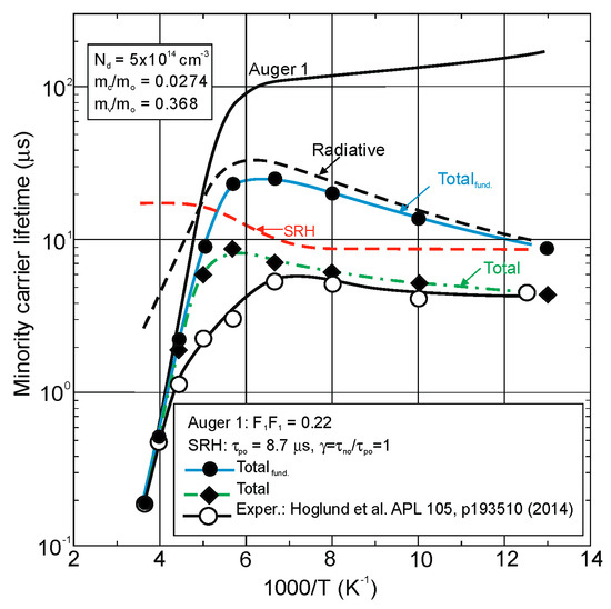
Figure 29.
Hole minority carrier lifetime versus inverse temperature for a n-type MWIR InAs/InAs0.54Sb0.46 T2SL with doping concentration 5 × 1014 cm−3 (after [114]).
The next two figures (Figure 30 and Figure 31) summarize carrier lifetimes data for bulk HgCdTe and both types of T2SLs (InAs/GaSb and InAs/InAsSb) operating in MWIR (λcut-off ≈ 5 μm), and LWIR (λcut-off ≈ 10 μm). The trend lines HgCdTe carrier lifetimes are given after Kinch et al. [115]. InAs/InAsSb SL system shows a significantly longer minority carrier lifetime (1 μs for MWIR material at 77 K) in comparison to the InAs/GaSb SL operating at the same wavelength range and temperature (~100 ns).
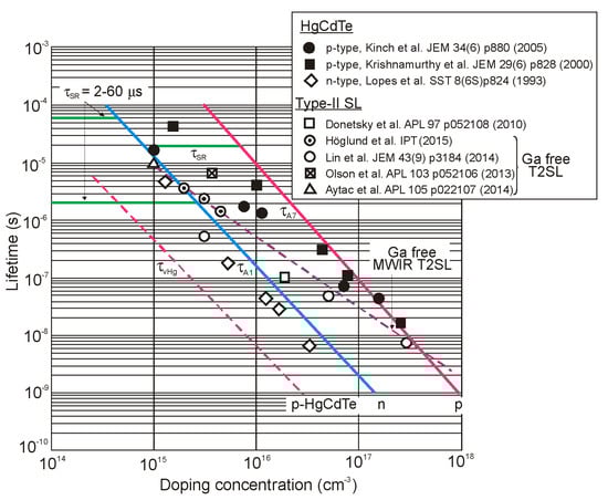
Figure 30.
Minority carrier lifetimes versus doping concentration for MWIR HgCdTe and T2SLs at 77 K. Theoretical trend lines for n-type and p-type HgCdTe ternary alloys are taken from [115]. The dashed line for Ga-free T2SLs follows experimental data.

Figure 31.
Minority carrier lifetimes versus doping concentration for LWIR HgCdTe and T2SLs at 77 K. Theoretical trend lines for n-type and p-type HgCdTe are taken from [115]. The dashed line for T2SLs follows experimental data.
In lightly doped n- and p-type HgCdTe, the SRH mechanism determines the carrier lifetime. Generally, values of τSRH are approximately more than two orders of magnitude larger for HgCdTe than those reported for the III-V semiconductors with similar bandgaps. At lower temperatures and doping level below 1014 cm−3, the HgCdTe P-i-N photodiodes become depletion limited due to SRH centers having lifetimes in the range to 10 ms [116,117]. In consequence, the potential properties of room-temperature HgCdTe photodiodes operating above 3 μm guarantee reaching more than order of magnitude higher detectivity (above 1010 Jones) in comparison with value predicted by Rule 07 [118], and this detectivity is limited by the background flux [119]. Up till now, long SRH lifetime of HgCdTe gives the potential to use this material system for background limited performance (BLIP) at room-temperature operation.
5. InAsSb Bulk Photodiodes
All epitaxial techniques require large area, single crystal, and lattice-matched substrates. Ternary and quaternary layers lattice matched to InAs or GaSb substrates could be tailored to detect wavelengths in the range of 0.8 to 5 μm. As shown in Figure 32, the GaxIn1–xAsySb1–y energy bandgap can be continuously tuned from ~475 to 730 meV while maintaining lattice-matching to a GaSb substrate [50,120], which is not retained for materials in this range such as InGaAs on InP. Both ternary (GaInSb and InAsSb) and quaternary (GaInAsSb and AlGaAsSb) materials, still not available on the market, show good performance for wavelength range ≥2 μm at the research level. The emergence of new GaInSb virtual substrates has created a promising potential for development of high performance IR detectors. Several research groups have succeeded in growing GaInSb single crystals, where there is a need to underline the properties of the Ga0.38In0.62Sb lattice matched to InAs0.35Sb0.65, with Sb composition providing the lowest energy bandgap.
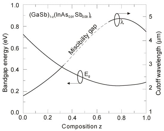
Figure 32.
The energy bandgap of GaxIn1−xAsySb1–y with x and y compositions chosen in the ratio (GaSb)1–z(InAs0.91 Sb0.09)z can be tuned continuously from ~475 to 730 meV while maintaining lattice-matching to a GaSb substrate.
5.1. Technology and Properties
A variety of InAsSb photodiodes configurations have been proposed during the last forty years including n-p, n-p+, p+-n and P-i-N structures in both planar and mesa configurations. In addition, the techniques used to form p-n junctions were different, starting of Zn diffusion, through Be ion implantation in LPE technique, to more advanced epitaxial techniques such as MBE and MOCVD. The last two are predominant in fabrication of modern antimonide-based IR detectors, that essentially relies on n-type material with concentrations ~1016 cm−3. A summary of works for the fabrication of InAsSb photodiodes is given in recently published monograph [88].
Considerable step in development of InAsSb photodiodes was obtained in 1980 when nearly lattice-matched system of InAs1−xSbx (0.09 ≤ x ≤ 0.15) and GaSb were used [9]. Slight lattice mismatch up to 0.25% for the InAs0.86Sb0.14 epitaxial layer was accommodated in terms of low etch-pit density (≈104 cm−2). Figure 33a shows a schematic structure of a back-side-illuminated (BSI) InAs1−xSbx/GaSb photodiode. The wider-gap GaSb is a transmission window for photons reaching the InAs1−xSbx active layer and where they are absorbed. Part of the photons is also absorbed in GaSb substrate, which determines the cut-on wavelength (1.7 μm at 77 K), while the active region establishes λcut-off = 4.3 μm (see Figure 33b). The InAs1−xSbx active layer was grown using LPE technique. Both undoped n-type layer and Zn doped p-type layer show the carrier concentrations of approximately 1016 cm−3. High quality of InAs0.86Sb0.14 photodiodes was demonstrated by a high RoA product in excess of 109 Ωcm2 at 77 K.

Figure 33.
BSI InAs0.86Sb0.14/GaSb photodiode: (a) device structure and energy-band diagram of the structure, (b) spectral response at 77 K (after [9]).
P-i-N heterostructure device with an unintentionally doped InAsSb active layer (π or ν; doping level ~1015 cm−3) sandwiched between P and N wider-bandgap layers have been proposed by several groups to improve device performance at near-room temperature operation. Lower diffusion dark current, higher RoA product, and detectivity are related to the lack of injection of minority carriers from the wide-bandgap layers. Figure 34 shows schematic architecture of the N-i-P heterostructure and the different combinations of III-V materials for an active and contact layers. For InAsSb absorber, usually p-type GaSb and n-type InAs are used for the contact layers. Depending on the configuration of contact layers, both BSI and front-side illumination (FSI) can be used. However, for the BSI photodiode, the transparency of the substrates is also crucial. In spite of the relatively low absorption coefficients of commonly used substrates (GaSb, InAs), they are thinned to small thicknesses, even less than 10 μm. Sometimes, the substrates are completely etched off. What is more, many fabrication processes are not possible for InAs due to its fragility. The transparency of the substrates can be improved by using a heavy n-type doping and the use of the BM effect. A strong degeneracy of the electrons in the CB occurs already for a relatively low electron concentration (>1017 cm−3). For example, in a heavily doped n+-InAs (Nd = 6 × 1018 cm−3), the BM shift makes the corresponding substrates transparent to the 3.3 μm [121].

Figure 34.
N-i-P double heterostructure photodiode schematic cross-section. Different combinations of III–V materials for active and cladding layers are also shown (after [91]).
In addition, many of the investigations were made in the Ioffe Physical-Technical Institute, see [121,122,123,124], on different antimonide-based ternary and quaternary alloys as a materials for MWIR double heterostructure (DH) photodiodes for near-room temperature operation. These DH devices with about several-μm thick undoped n-InAs1−xSbx active layers and p-InAs1−x−ySbxPy 3-μm-thick Zn-doped cladding contact layers are LPE grown on n-type InAs(100) substrates (with n = 2 × 1016 cm−3 for undoped or n+ = 2 × 1018 cm−3 for the Sn-doped substrates). For example, Figure 35 presents the distribution of P, Zn, Sn, and Sb atoms along the growth direction of the BSI P-InAsSbP(Zn)/p-InAs0.88Sb0.12(Zn)/n-InAs0.88Sb0.12/n+-InAs(Sn) DH photodiode obtained by the secondary ion mass spectroscopy (SIMS). InAs0.88Sb0.12 absorber with smooth Zn distribution in the vicinity of the p-n junction is optimized for the MWIR range.

Figure 35.
Distribution of P, Zn, Sn, and Sb atoms along the growth direction (SIMS data) of LPE-grown P-InAsSbP(Zn)/p-InAs0.88Sb0.12 (Zn)/n-InAs0.88Sb0.12/n+-InAs(Sn) DH photodiode. Arrows on the right and left denote photon flux with respect to heterostructure layers at the photoluminescence (PL), photodiode (PD), and electroluminescence (EL) modes (after [125]).
Figure 36 shows the detector dimensional dependence of dark currents for the InAsSbP/InAs0.7Sb0.3 DH photodiodes fabricated in Ioffe Institute with active 3-μm thick n-type InAsSb region. High circular mesas were defined by a standard optical photolithography and a wet chemical etching process. Next, circular Au- or Ag-based reflective anode and cathode contacts were formed by sputtering and thermal evaporation in vacuum. Finally, flip-chip bonding/packaging procedure has been implemented. Some chips were equipped with aplanatic hyperhemispherical Si immersion lenses (Ø = 3.5 mm) with antireflection coating. After [126], InAsSbP/InAs0.7Sb0.3 DH photodiodes demonstrate diffusion-limited current at near room temperature and tunnel current at 212–250 K with predominantly series resistance in the temperature range of 270–300 K. At a room-temperature, the surface leakage current dominates the bulk one starting at mesa diameter less than ≈ 17 μm. As is marked in Section 3.3, the surface of semiconductor like InAs (also bulk InAsSb and InAs/InAsSb T2SLs) exhibits n-type conductivity even when the material is p-doped. After etching, the detector pixels contain exposed side-walls with a p-n+ surface junction when absorber is doped on a p-type. Thus, for good performance, such detectors would require passivation.
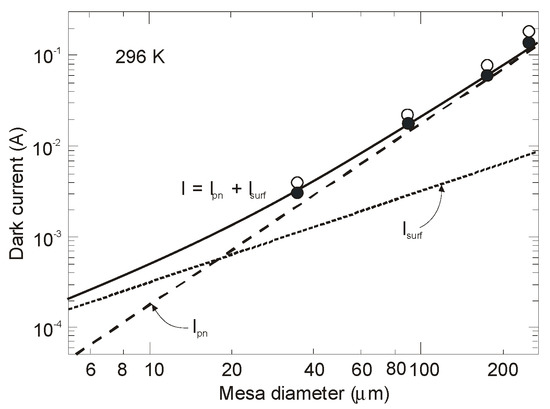
Figure 36.
Total dark current at a reverse bias of 0.1 V (•) and 0.2 V (○) in InAsSbP/InAs0.7Sb0.3 DH photodiode at room temperature. The lines present the simulated bulk (Ipn) and surface (Isurf) leakage currents as well the sum of the above two currents at a reverse bias of 0.1 V (after [126]).
Figure 37 summarizes experimental data of RoA product versus photon energy for n+-InAs/n-InAsSb/p-InAsSbP DH photodiodes in wide wavelength spectral range to 9 μm. The experimental data for InAsSb photodiodes are comparable with those of HgCdTe photodiodes produced by VIGO System. It is assumed that the photon energy in the region of 90% photocurrent drop is being close to the energy gap of photodiode active region. An exponential dependence of RoA product, approximated by exp(hν0.1/kT), shows that the transport properties are determined by the diffusion current and the leakage current flow mechanism is negligible.
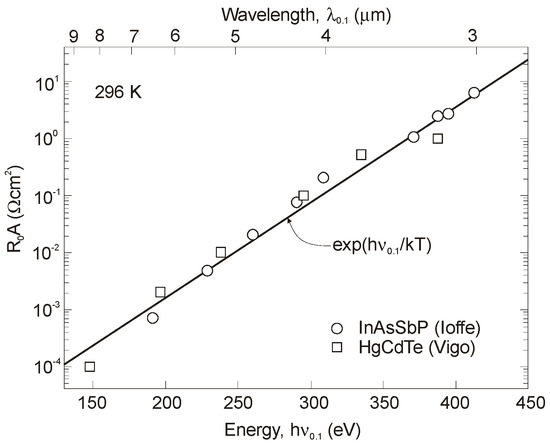
Figure 37.
RoA product in series of InAsSb DH at room temperature (after [127]).
The final construction of immersion photodiode is similar to that shown in Figure 38a [123]. Figure 38b shows the Johnson-limited detectivity at different temperatures of InAsSb DH photodiodes with immersion lenses. As seen from this figure, on the spectral responsivity characteristics, four distinct regions can be distinguished: region of a rapid responsivity decay in the wavelength range from 4.7 μm to 5.5 μm, so called the cut-off region (1), highest responsivity region with a sharp longwave response decline (2), smooth response decline region (3), and finally fast shortwave response decline region, so called cut-on region (4). A short-wave responsivity limit depends on the transparency of the substrate. In the case of a highly doped n+-InAs substrate, the BM effect shifts the detector response by 1 µm towards the shorter wavelengths (see difference in short wavelength spectral responsivity between heavily doped-#878 sample and undoped-#877 sample).
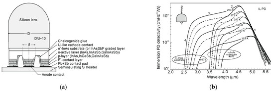
Figure 38.
DH InAsSb immersion photodiodes: (a) construction of the immersion photodiode (after [121]) and (b) detectivity spectra at different temperatures for InAsSb photodiodes with n-InAs and n+-InAs substrates (after [123]).
Figure 39a summarizes the peak detectivity of photodiodes in dependence of temperature. The next figure, Figure 39b, presents detectivities in dependence on peak wavelength for the flat BSI photodiodes and the immersion lens photodiodes (immersion illuminated—IL). For the immersion lens photodiodes, the peak detectivities are generally about one order of magnitude higher than those for bare chip PDs-see Figure 39b. The photodiodes developed at the Ioffe Institute are superior to the majority published in literature. At the same time, the RoA products are lower than that given in [8].
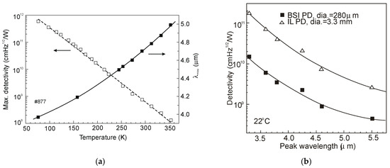
Figure 39.
Detectivity of InAsSb DH photodiodes: (a) maximum detectivity and peak wavelength versus temperature (after [123]); (b) peak detectivity versus peak wavelength of photodiodes without (BSI) and with Si lenses (IL) (after [121]).
More recently, the Ioffe’s research group has demonstrated the InAsSbP/InAs0.7Sb0.3 DH photodiodes grown onto InAs substrates with peak responsivity about 6.5 μm. Their spectral current responsivity in temperature range between 233 K and 330 K is shown in Figure 40a. The Jonson noise limited detectivity at 233 K, achievable by a 2-stage thermoelectric cooler, is 3.2 × 10⁸ cmHz1/2/W at λ = 6.5 μm. The use of the integrated with photodiode a hyperhemispherical immersion Si lens (Ø = 3.5 mm) increases the D* value to 4.3 × 10⁹ cmHz1/2/W (see Figure 40b).

Figure 40.
DH InAsSbP/InAs0.7Sb0.3 p-n photodiodes grown onto InAs substrates: (a) photoresponse spectra in the 233–330 K interval, (b) maximum detectivity for bare chip (⧠) and immersion lens (○) photodiodes (left scale) and responsivity (right scale,) versus temperature in a 195-µm wide bare chip (after [125]).
5.2. Performance Limits
Despite the promise of the III-V based detectors, HgCdTe remains the highest-performing IR material technology for a number of applications. High-quality InAsSb photodiodes optimized for the 3–5 μm spectral region with performance comparable to HgCdTe have been developed over the last 30 years. However, a long-standing hope that the InAsSb might become a useful material in 8–12 μm spectral band has still not been realized. In comparison with HgCdTe, the main obstacles to achieving this goal are: poor quality crystal structure (there is no ideal III–V substrate/epitaxial combination that is appropriate for LWIR spectral band), poor SRH lifetimes, and relatively high background carrier concentration (lowest at the level of 5 × 1014 cm−3). Moreover, the observed energy gaps of InAs1−xSbx with middle Sb compositions (close to minimum energy gap (see Figure 4 and Figure 5)) are not inherent and well controlled due to CuPt-type ordering and residual strain effects. The design of buffer layer and its thickness have strong impact on the RoA product and spectral responsivity [126].
The RoA product is a commonly encountered figure of merit for a photovoltaic detector and is defined as
at zero-biased voltage Vb = 0. Here J = I/A is the current density, and A is the detector area.
Rogalski et al. have reported a theoretical analysis of MWIR InAs1−xSbx (0 ≤ x ≤ 0.4) photodiodes with operation extending to the temperature range of 200–300 K [128]. Figure 41 presents a theoretical critical value of the RoA product for InAsSb DH photodiodes operating at 200 and 300 K and in spectral range between 3 and 8 μm. With the current state of technology, the electron concentration in the undoped absorber is at the level of 1015–1016 cm−3, thus the theoretical calculations have been done for two doping close to the level available in practice. For comparison with theoretical predictions, only limited experimental data published to 1996 is marked. The agreement is satisfactory assuming 15-μm thick base region of photodiode (solid lines). However, as is shown in this figure, the room-temperature experimental results published recently in [127], are located above theoretically predicted line. The main reason of this discrepancy is considerably lower thickness of active region-typically 4 μm. By reducing the photodiode volume in which diffusion current is generated, the corresponding RoA product increases by a factor of Lh/d [3], where Ld is the minority diffusion length and d is the thickness of base region.

Figure 41.
The RoA product versus λcut-off for InAs1−xSbx DH photodiodes at temperatures 200 and 300 K. The solid curves are calculated for two doping concentrations (1015 cm−3 and 1016 cm−3) in the active region of photodiode with a thickness of 15 μm; the carrier concentration of 1018 cm−3 in p+-cap layer with thickness equal 1 μm is assumed. The experimental data are taken from [127] (∎), [129] (o), [130] (•), [131] (□), and [132].
More recently, Wróbel et al. have considered the effects of doping profiles on room temperature MWIR InAsSb photodiode parameters (RoA product and detectivity) [91]. In theoretical estimates a new dependence of the spin-orbit-splitting energy on the Sb molar composition was taken into account [89] -see Figure 17. Figure 42 shows the dependence of the RoA product on the λcut-off for InAs1−xSbx p-on-n and n-on-p photodiodes at 300 K. Electron and hole concentration in a 5-µm thick active regions, respectively in p-on-n and n-on-p photodiode, was assumed at the level of 1016 cm−3. It is clearly shown that in the photodiode with p-type active region with a Sb composition close to InAs (0 ≤ x ≤ 0.15; λcut-off < 4.5 µm), Auger S mechanism considerably decreases RoA product in comparison with the photodiode with n-type absorber, in which Auger S mechanism is not significant. However, for longer wavelengths (x ≥ 0.15; λcut-off > 4.5 µm), the n-on-p photodiode is more optimal than p-on-n one.
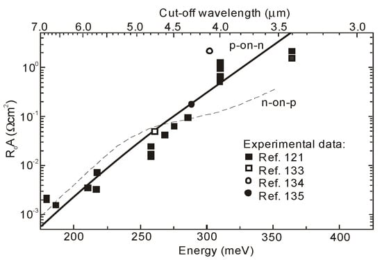
Figure 42.
The RoA product versus λcut-off for InAs1−xSbx p-on-n and n-on-p photodiodes at room temperature. The theoretical lines are calculated for doping concentration of 1016 cm−3 in both p- and n-type 5-µm thick absorber. The gathered experimental data concerns p-on-n photodiodes with n-type active region (after [91]).
The theoretical relations presented in Figure 42 were also compared with the experimental values for the p-on-n photodiode. A good agreement between both types of data was obtained, even though some experimental points are located above the theoretical line. This can probably be observed if the thickness of the active region is less than the diffusion length of the minority carriers.
Knowing the RoA product, the normalized detectivity limited by the thermal noise can be calculated using formula
assuming QE, η = 0.7.
The next figure (Figure 43) shows experimental and theoretical normalized detectivity of p-on-n InAsSb photodiodes operating at room-temperature and different λcut-off. The discrepancy between experimental data and theoretical prediction increases versus λcut-off. It may be caused by decrease of measured QE, while the theoretical was assumed to be constant.

Figure 43.
Normalized detectivity versus λcut-off for InAs1−xSbx p-on-n and n-on-p photodiodes at room temperature. The theoretical line is calculated for 5-µm thick active region with doping concentration of 1016 cm−3. The gathered experimental data is taken from literature (after [91,121,133,134,135,136]).
Figure 44 compares the experimental detectivity values of commercially available different types of InAsSb photodetectors (mainly photodiodes) operating at room temperature with experimentally measured HgCdTe photodiodes and theoretically predicted curves for P-i-N higher operating temperature (HOT) HgCdTe photodiodes. All experimental data gathered in this figure indicates on the sub-BLIP photodetectors’ performance. As is shown, the best quality HOT photodiodes are fabricated by Teledyne Judson Technologies with detectivity about one order below BLIP curve for λcut-off ~5 μm.
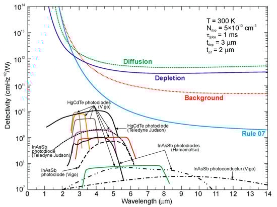
Figure 44.
Detectivity on wavelength dependence for the commercially available room-temperature HgCdTe photodiodes and InAsSb photodetectors [137,138,139,140]. The theoretical curves are calculated for P-i-N HOT HgCdTe photodiodes assuming the value of τSRH = 1 ms, the absorber doping level of 5 × 1013 cm−3 and the thickness of active region t = 5 µm (tdif-diffusion thickness, tdep-depletion thickness) [119].
At present stage of the HgCdTe technology, the “Rule 07” metric (specified in 2007 [118]) is not a proper approach for prediction of the HgCdTe detector and system performance and as a reference benchmark for alternative technologies. The Rule 07 coincides well with theoretically predicted curve for Auger-suppressed p-on-n photodiode with electron concentration in active region ~1015 cm−3. For sufficiently long SRH carrier lifetime in HgCdTe, which is experimentally supported at doping level below 5 × 1013 cm−3, the internal P-i-N HgCdTe photodiode current is suppressed and performance is limited by the background radiation [117]. In Extended Abstracts of The 2019 U.S. Workshop on the Physics and Chemistry of II-VI Materials [132], it was suggested to replace “Rule 07” with “Law 19”. The “Law 19” corresponds exactly with the BLIP curve for room temperature [117]. The internal photodiode current can be several orders of magnitude below “Rule 07” versus λcut-off and operating temperature. In this context, the alternative technologies should be considered and evaluated.
Figure 44 shows that the potential properties of HOT HgCdTe photodiodes operating in longer wavelength IR range (above 3 μm) guarantee achieving more than order of magnitude higher detectivity (above 1010 Jones) in comparison with value predicted by “Rule 07” [119]. The above estimates provide further mobilization for achieving high performance MWIR and LWIR HgCdTe FPAs operating in HOT conditions, at low production costs. In the most optimistic scenario, antimonide/arsenide-based photodetectors can totally supplant the Hg1−xCdxTe devices for each spectral range and operating temperature. Particular fabrication efforts provide Hamamatsu with a variety of IR detectors with different spectra response characteristics-see Figure 45.
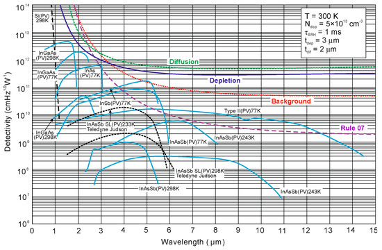
Figure 45.
Spectral detectivity curves of commercially available photovoltaic (PV) detectors at different temperatures (after [140]). The theoretical curves are calculated for P-i-N HOT HgCdTe photodiodes assuming the value of τSRH = 1 ms, the absorber doping level of 5 × 1013 cm−3, and the thickness of active region t = 5 µm [119].
5.3. Barrier Detectors
The first barrier detector was proposed by A.M. White in 1983 [141] as a high impedance photoconductor. Its design was similar to the currently used nBn detector: a thin wide bandgap layer was placed between a bandgap gap n-type absorber region and the same narrow bandgap contact region. A.M. White in his prescient patent also proposed a bias-selectable two-color detector realized and exploited currently in HgCdTe and in the T2SL material systems.
The barrier detector principle of operation is to allow the flow of one carrier type (electron or hole), while blocking the others-hence the term “unipolar barrier”. Thus, the concept of unipolar barrier assumes almost zero offset approximation throughout the heterostructure in one band and a high barrier in the other band. The most popular between different types of unipolar barrier detectors is the nBn detector.
A typical nBn concept assumes a uniform n-type doping through the heterostructure (see Figure 46a), which is key to maintain a low, diffusion limited dark current. From one side of the unipolar barrier (B) is a narrow-bandgap semiconductor which constitutes the photon-absorbing layer with a thickness comparable to the absorption length of light in the device, typically several microns. The narrow-bandgap semiconductor on the other side of the barrier plays a role of a contact layer for device biasing. Barrier should be located near the minority carrier collector and away from the region of optical absorption. As mentioned, the barrier needs to be carefully engineered. A nearly zero VBO should allow photogenerated holes to flow to the contact (cathode), while large offset in the CB should block majority carrier dark current, reinjected photocurrent.

Figure 46.
Bandgap diagram of nBnn (a) and nBpn (b) barrier detectors (Δ-VBO) and p-n photodiode (c).
The nBn detector can be considered as a hybrid of the p-n photodiode and the photoconductor. The p-n junction (space charge area) (see Figure 46c) is replaced by the barrier, and p contact is replaced by the n-type layer. Due to the absence of majority carrier flow, in this respect it is similar to a photoconductor with unity gain.
The operating principles of the nBn and related detectors have been widely demonstrated in the literature [101,142,143,144,145,146,147,148,149,150]. The idea of nBn concept has originated with bulk InAs [142]. However, it is difficult to realize little or no VBO using this material and other bulk IR detector materials such as InSb and HgCdTe. In the middle of first decade of the XXI century, the IR technology has changed after the introduction of 6.1 Å III-V material family and first demonstration of high-performance detectors and FPAs [142,143]. The introduction of broken-gap T2SLs was particularly helpful in the design of unipolar barriers, as they enable any modification of the detector architecture with better control of band edge alignments [151]. The ability to tune the positions of the CB and VB edges independently is easier than in bulk materials.
In general, unipolar barriers architecture is used to increase the photogenerated carriers’ collection efficiency, reduce dark current (associated with SRH processes), and noise without inhibiting photocurrent flow. In particular, the barrier plays a role of self-passivation and serves to reduce the surface leakage current. Other key benefits of uniform doping of nBn detector (n-type barrier, Bn) is the absence of depletion regions in the narrow-gap absorption layer. It offers a way for materials with relatively poor SRH lifetimes, such as all III-V compounds, to grow on lattice-mismatched substrates such as GaAs, with a reduced penalty of excess of the dark current generated by SRH centers associated with dislocations.
The papers [144,145] established a criterion for combination of voltage and barrier doping concentration allowing operation with no depletion region in the narrow gap active layer. In some material system, a barrier in the VB is present when the barrier layer is n-type (Bn), that can significantly impede hole current flow from absorber to the contact layer. In such situation, a relatively high voltage (so called “turn-on voltage”) is required to overcome. A p-type doping of the barrier, Bp, helps to reduce the barrier in the VB (see Figure 46b) but rather a potential well for holes in the VB which does not impede hole transport between the absorption layer and the contact layer. However, in the last case, a p-type barrier layer inherently causes depletion regions to form in the narrow-gap absorption layer for all voltages, what should be avoided (depletion regions cause excessive G-R dark currents).
Detailed growth procedures and device characterization of MWIR detectors based on InAsSb/AlAsSb material system were published in several papers, e.g., References [144,145,147,152,153]. The principal layers of the device structures were n-type doped and consisted of a thick InAs1−xSbx absorption layer (1.5–3 μm), a thin AlAs1−xSbx barrier layer (0.2–0.35 μm), and a thin (0.2–0.3 μm) InAs1−xSbx contact layer. The bottom contact layer was highly doped. InAsSb/AlAsSb nBn structures were grown on either GaAs(100) or GaSb(100) substrates by using MBE technique [153]. The n-type doping was usually obtained by either Si or Te elements. The remaining structures were grown directly onto lattice-matched GaSb (100) substrates, while lattice-mismatched GaAs (100) substrates were used, structures were grown on a 4-μm thick GaSb buffer layer.
Figure 47a shows an example of such an nBn structure that was theoretically investigated by Martyniuk and Rogalski [154]. The alloy compositions of x = 0.09 to 0.2 for the InAs1−xSbx absorber layers provided the λcut-off wavelengths of ~4.1 to ~5.0 μm at 150 K, respectively. The current-voltage characteristics were taken from [155]. The dark current density for nBn InAs0.805Sb0.195 structure was 1.0 × 10⁻³ A/cm2 at 200 K and 3.0 × 10⁻⁶ A/cm2 at 150 K.

Figure 47.
InAsSb/AlAsSb nBn MWIR detector: (a) the device structure ([154]), (b) dark current density versus voltage for InAs0.805Sb0.195 for selected temperatures 4096 (18 µm pitch) detectors (λcut-off ≈ 4.9 µm at 150 K) tied together in parallel (after [155]), and (c) schematic Arrhenius plot of temperature dependence of the dark current in two type InSb p-n junctions (made by ion-implantation and MBE grown (dashed line). The diffusion and G-R limited portions of the InAsSb curves are also labeled.
In nBn InAsSb detector, the depletion current is totally suppressed (see Figure 47c) because there is no depletion region. In the low-temperature region, for temperatures below Tc, the nBn detector exhibits a higher signal-to-noise ratio in comparison with the conventional p-n diode operating at the same temperature, or otherwise the nBn detector can operate at a higher temperature than a conventional p-n diode with the same value of dark current. InAsSb p-n photodiode is characterized by a higher crossover temperature, Tc, between diffusion and G-R contribution than InSb, which results from the larger bandgap of InAsSb than InSb (only in a certain range of Sb molar composition, for InAsSb close to InAs).
In InAsSb nBn detector (n-type absorber), the dark current density limited by the Auger 1 and SRH mechanisms can be calculated as
where Nd and t are the doping and thickness of active region, respectively. The influence of G-R current associated with a depletion region (Jdep = qniw/τSRH, were w is the depletion width) can be omitted.
According to Equation (14), the Auger 1 generation varies as Nd, whereas the SRH generation varies as 1/Nd. It follows that that the diffusion dark current mostly depends on absorber doping concentration and on value of SRH lifetime. Kinch has modeled the diffusion current in an InAsSb absorber versus doping concentration at 150 K (assuming τSRH = 400 ns (see Figure 19) and an absorber thickness of 3 μm). As is shown in Figure 48a, the optimum doping is 1016 cm−3. Next, Figure 48b shows the dark current density for InAs0.91Sb0.09 absorber versus inverse temperature for doping concentration 5 × 1015 cm−3. This figure shows that the dark current is equal to the f/3 background flux at temperature of ~175 K. At 150 K, the dark current density is 2 × 10⁻⁷ A/cm2, in agreement with experimental nBn InAsSb data [156]. In this way, the nBn InAsSb detector operating with f/3 optics reaches BLIP for T > 160 K (temperature two times higher than traditional InSb).
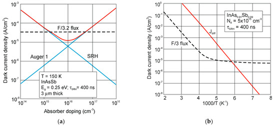
Figure 48.
Dark current density for InAsSb nBn absorber (τSRH = 400 ns, t = 3 µm): (a) versus doping concentration, and (b) versus inverse temperature for a donor doping 5 × 1015 cm−3 (after [78]).
Interesting difference in dark current density versus temperature is shown in Figure 49 for two nominally identical nBn devices, each operating at a bias of −0.1 V. The devices differ only in the doping of the barrier layer. The nBnn device with a uniform n-type doping through the entire structure exhibits a single straight line, typical for the diffusion limited behavior. The nBpn device, with a barrier doped opposite to the absorber, exhibits two-slope behavior, typical for the diffusion limited mode at high temperatures and the G-R limited behavior at low temperatures. As is shown, the dark current density at 150 K is more than two orders of magnitude greater for the device with the p-type due to the presence of the depletion region. It appears that for a typical QE of 70% at f/3 optics, the BLIP temperature is about 140 K compared with ~175 K for the detector with the n-type barrier.
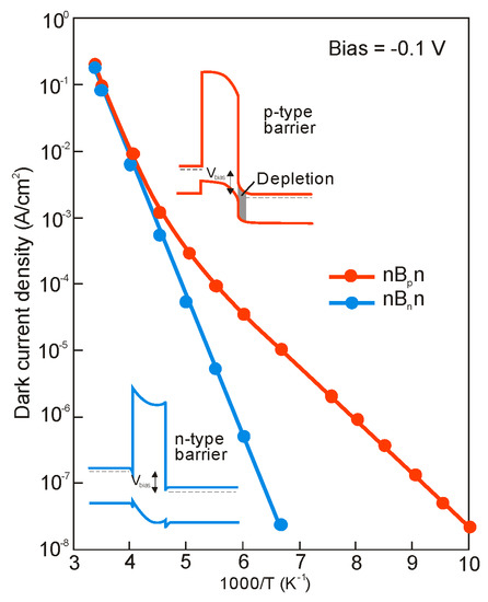
Figure 49.
Dark current density vs. temperature for two identical InAsSb/AlSbAs nBn devices with opposite barrier doping. Active layer bandgap wavelength is 4.1 µm at 150 K (after [150]).
Over present-day IR technologies, InAsSb-based barrier detectors offer numerous advantages, such as reduced depletion and surface leakage currents, normal-incidence absorption. However, the promise of the excellent performance of these detectors has yet to be practically realized. Martyniuk and Rogalski have predicted the temperature dependencies of dark currents of different types of IR detectors, including InAsSb nBn detectors, optimized at a λcut-off = 5 μm [157].
The advantages of the nBn structure, compared to the InAsSb photodiode with the built-in depletion region, are clearly visible. The nBn structure enables operation at much higher temperatures while maintaining the same dark current values (see Figure 50). However, still these values are not comparable to the HgCdTe photodiodes with p-on-n or even n-on-p design. More comparable to HgCdTe photodiodes is T2SL InAs/InAsSb nBn detector. MWIR HgCdTe systems operating at f/3 optics at 160 K are commercially available.
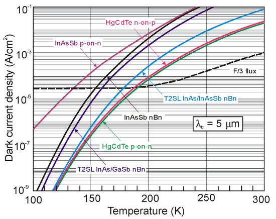
Figure 50.
Dark current density versus temperature for InAsSb p-on-n photodiode and nBn detector, T2SL nBn detectors, and HgCdTe photodiodes with λcut-off = 5 µm.
Early efforts in development of InAsSb barriers detectors focused on lattice-matched structures to GaSb substrates with λcut-off ~ 4.1 μm. Different strategies were attempted to extend the λcut-off above 5 μm including various metamorphic buffer layers and InSb interface ML into the InAsSb [158,159]. It appears that the activation energies estimated from temperature dependence of dark currents is higher than the bandgap of InAsSb absorbers, which is explained by location of the accumulation layer between the barrier and absorber due to band bending [160]. Some barrier detectors also exhibits an increase in the turn-on bias versus temperature as a result of the Fermi level position changes in low-doped or unintentionally doped absorbers. At higher temperature, a higher voltage is needed to deplete the barrier-absorber interface region [161].
Lin et al. [42] have described bulk InAsSb barrier detectors with a λcut-off about 10 μm at 77 K. The estimated InAs0.60Sb0.40 absorber parameters at 77 K are as follows: the hole mobility of 103 cm2/Vs, the minority hole lifetime of 185 ns, and the diffusion length of 9 μm. The current-voltage characteristics have been influenced by G-R component associated with a depletion region adjacent to the barrier, as well as probably tunneling components. To reach diffusion-limited dark current, the VBO associated with the heterointerfaces must be eliminated.
The spectral detectivity curves of LWIR nBn InAsSb detector, with two absorber’s doping levels, are shown in Figure 51. The demonstrated detectivity of 2 × 10¹¹ cmHz1/2/W at 2π FOV and wavelength of 8 μm was estimated in spite of the significant shift towards shorter wavelengths (BM shift) with doping. For 1 μm thick InAs0.60Sb0.40 absorber at λ = 8 μm, an absorption coefficient was estimated at 3 × 103 cm−1, what implies QE = 22%. The QE increases with bias, until it reaches a constant level for −0.4 V and with thickness of absorption layer (to 40% for 3-μm thick absorber). Generally, due to poor quality crystal structure, the performance of LWIR bulk InAsSb detectors are considerably inferior in comparison with HgCdTe photodiodes.
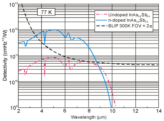
Figure 51.
Spectral detectivity of barrier detectors with 1 µm thick InAs0.6Sb0.4 absorbers at T = 77 K. Dashed and solid lines represent devices with undoped and n-type doped absorbers, respectively. Dotted line shows the 300 K BLIP limit for a 2π FOV (after [42]).
6. InAs/InAsSb Superlattice Detectors
Development of the T2SLs has more than forty years history. Figure 52 gives it a short description in the form of a timeline, including InAs/InAsSb SLs. The development of InAs/InAsSb SLs for IR detector applications is described in detail in several papers [19,21,159,162]. It has a long and interesting history that predates the InAs/GaSb SL detectors. Up till 2010 this material system was much less explored than the T2SLs InAs/GaSb. In the last decade, a rapid progress in their fabrication is made due to some defect tolerance and its robust material properties. In general, the growth of the InAs/InAsSb T2SLs is easier compared to the InAs/GaSb ones and InAs/InAsSb SLs have longer minority carrier lifetimes (see Section 4.3). On the other hand, its spectral tuneability is somewhat smaller and the InAs/InAsSb T2SLs has weaker optical absorption. In addition, vertical hole transport properties, especially in the LWIR range, are more challenging.

Figure 52.
Roadmap development of T2SL IR photodetectors including InAs/InAsSb SL photodiodes and barrier detectors.
6.1. Performance Limits
The InAs/GaSb SL detectors are most commonly designed with p-type absorbers, while in the case of InAs/InAsSb SL detectors, it is better to use an n-type absorber due to their surface properties. In InAs/InAsSb SLs, the surface Fermi level is pinned above the CB minimum, resulting in a degenerate n-type surface. Thus, for the n-type absorber no special surface treatment is required since the surface band-bending potential repels the minority carriers (holes) away from the surface. In a p-type absorber, the minority electrons are attracted to the n-type surface contributing to the surface leakage current. In addition, the depletion region in the surface p-n+ junction is a source of both G-R and tunneling dark currents.
Summarizing the above discussion-choosing between the two types of SLs, InAs/GaSb and InAs/InAsSb, it is necessary to take into account the λcut-off, the ease of growth technology and processing capabilities (including passivation). In general, the InAs/InAsSb SLs are more effective for implementation in the MWIR range, where they could have an advantage over the InAs/GaSb ones.
Figure 50 and Figure 53 compare the predicted dependence of dark current density on operating temperature for different material systems including InAs/InAsSb SLs with λcut-off of 5 and 10 µm. The LWIR InAs/GaSb T2SL materials have larger dark current densities than HgCdTe. Their inferior parameters appear to result from a relatively high background concentrations (about 1015 cm−3) and a shorter minority carrier lifetime. The BLIP performance with f/1 optics for InAs/InAsSb nBn detector is achieved at about 130 K and is close to HgCdTe photodiode.

Figure 53.
Dark current density versus temperature for T2SL nBn detectors and HgCdTe photodiodes with a λcut-off = 10 µm.
Figure 54 compares the RoA and RdA values for InAs/InAsSb SL and HgCdTe devices operating in a wide IR spectral range. For good photoresponse of the nBn detectors, the devices must be biased typically in the range above −100 mV. Thus, the RdA product is used instead of the RoA, where Rd is the dynamic resistance at non-zero bias voltage. The solid line is the trend line calculated with Teledyne empirical model (“Rule 07” [118]) for P-on-n HgCdTe structures. The HgCdTe experimental data are given for photodiodes fabricated by Raytheon Vision Systems (RVS). As we can see, the upper results for InAs/InAsSb SL detectors rival that of practical HgCdTe devices.
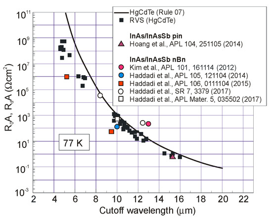
Figure 54.
RoA and RdA product of nonbarrier and barrier T2SL InAs/InAsSb detectors on λcut-off wavelength dependence compared to experimental data and trend line (“Rule 07”) for HgCdTe photodiodes at 77 K. The experimental data for InAs/InAsSb SLs devices are taken from [163,164,165,166,167,168].
In the case of InAs/InAsSb SL barrier detectors having a λcut-off ~12 µm, the values of RoA > 102 cm2 at 77 K are measured. These values are higher than those measured for HgCdTe photodiodes. Generally, however, the InAs/InAsSb SL detectors are characterized by lower QE ~ 40–50% (see Figure 55) than HgCdTe photodiodes (>70%), mainly due to lower absorption coefficient.

Figure 55.
QE versus thickness of active region for InAs/InAs1−xSbx T2SL photodetectors at 77 K. The theoretical prediction (solid line) is compared with the experimental QE reported by different research groups as indicated inside the figure (adapted after [169]).
The main technological challenge for the fabrication of SL-based devices is the growth of high-quality active region with sufficient thickness to achieve satisfactory QE. For InAs/InAsSb photodetectors, 5 µm thick absorber is sufficient to provide high enough QE. It may provide QE about 50%, due to a longer effective lifetime and diffusion length, in comparison with InAs/GaSb SLs. Figure 54 shows the theoretical QE of InAs/InAsSb T2SL detectors versus the absorber thickness, calculated for the effective carrier lifetime of 150 ns [169]. Table 4 summarizes reports of InAs/InAsSb-based SL IR detector results.
Table 4.
InAs/InAsSb superlattice infrared detectors.
Figure 56 shows the comparison of the simulated detectivity of P-on-n HgCdTe photodiodes versus λcut-off and operating temperature with the experimental data T2SL InAs/InAsSb photodetectors operating at 78 K, 150 K and 200 K. The solid lines present theoretical thermal limited detectivity for HgCdTe photodiodes, modeled using the “Rule 07” dark current density. This figure indicates that the measured thermally limited detectivity of T2SLs InAs/InAsSb photodetectors exhibits lower performance in comparison to the HgCdTe photodiodes not even reaching the HgCdTe level. That is mainly related to the fairly high background concentrations (~1 × 1015 cm−3) and a lower absorption coefficient and in consequence lower QE. Improvement in those two fundamental parameters seems to be critical to reach the theoretically predicted T2SLs photodiodes performance.
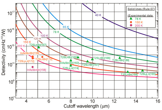
Figure 56.
The simulated detectivity of the P-on-n HgCdTe detectors (Rule 07, QE = 70%) versus λcut-off and temperature. The experimental data is taken with different sources (as marked) for InAs/InAsSb T2SL photodetectors operating at 78 K, 150 K, and 200 K.
6.2. Superlattice Detector Structures
The majority of the T2SL devices are grown by MBE being expensive for mass production, while the recent interest in T2SLs growth by MOCVD is observed which is related to the low-cost and versatile production guaranteed by that technique [173,174].
In the last decade, the particular contribution in development of T2SLs InAs/InAsSb detectors and FPAs has given two research groups; group at Jet Propulsion Laboratory (JPL) [107,158,159,161,171,172] and the Razeghi group from Northwestern University [164,165,166,167,168,173,174]. Both groups have demonstrated the versatility of the T2SLs InAs/InAsSb with operating λcut-off ranging from 2 to 14 μm and beyond. In this way, SLs material expends the limited spectral range covered by traditional bulk III-V IR detectors based on InGaAs and InSb.
Table 4 indicates that the T2SLs InAs/InAsSb detectors are fabricated mainly in two configurations: p-n junction photodiodes (impurity diffusion [178], MBE [164], MOCVD [173,174]) and nBn barrier detectors (mainly MBE). The T2SL InAs/InAsSb photodiodes, as shown in Figure 34, are mainly constructed on P-i-N heterostructures. The low minority carrier concentration in the high bandgap materials allows for the suppression of diffusion dark current and reaching higher RdA product and detectivity.
In comparison with the p-n junction T2SLs InAs/InAsSb photodiodes, SLs IR barrier devices are more effective (see Figure 50 and Figure 53). As is described in Section 5, the unipolar barrier structures allow reducing G-R dark current by suppressing SRH mechanism and surface leakage. That is particularly useful for the p-n devices based on III-V materials, inherently exhibiting excessive depletion dark current and suffering from the lack of proper surface passivation.
InAsSb-based bulk and SLs photodetector performance has been increased by the monolithically integrated microlenses based on GaAs/GaSb substrates [180,181]. The hemispherical or hyperhemispherical microlenses increase the effective detector’s optical area by of , respectively, where nr is the index of refraction of the lenses [182]. The detectivity gain achieved with hyperhemispherical immersion is . Since the refractive index of GaAs is 3.4, a factor of 10 improvements in the detectivity is observed for n-type and p-type InAsSb absorbers [180]. Figure 57 shows the immersion lens formed from GaAs substrates using numerically controlled micromachining.

Figure 57.
The photodetector assembled on the 3-stage Peltier thermoelectrical cooler and GaAs immersion microlens. The improvement in detectivity reached by hyperhemispherical microlens is proportional to , where nr is the GaAs refractive index (after [180]).
The nBn (pBp) detector design is also useful for the realization of dual-band detection capabilities shown schematically in Figure 58. The dual-band barrier structures could be easily fabricated due to the highly developed III-V materials growth techniques. Typical dual-band, barrier T2SLs detector consist of the two narrow bandgap absorbers optimized for the two different IR spectral regions being separated by ~0.1 μm thick wide bandgap barrier for majority carriers (no barrier for minority carriers is assumed). That architecture blocks the majority carrier current between the two electrodes by the large energy offset, while there is no barrier for photo-generated minority carriers. Both barriers should be characterized by negligibly small VB or CB discontinuity with respect to both n-type (p-type) doped active regions. The absorbers (channels) are addressed consequently by the polarity of the applied voltage. Detector with pBp design exhibits faster operation with lower integration times, due to the higher minority carrier mobility (electrons).
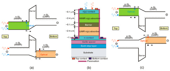
Figure 58.
Schematic of nBn (a) and pBp (c) T2SL dual-band detector operations under forward and reverse bias. Schematic view of dual-band MWIR/LWIR detector architecture is shown in centre (b).
Krishna et al. have demonstrated two-color barrier detectors based on nBn or pBp InAs/GaSb SL architectures [183,184]. Furthermore, their improvement in InAs/InAsSb two-band SL fabrication was demonstrated in [166,168].
6.2.1. Photodiodes
Both MWIR [174,185] and LWIR [164,173] T2SLs InAs/InAsSb photodiodes have been demonstrated. The experimentally measured dark current density of MWIR photodiodes with a λcut-off = 5.4 μm at 77K, was found larger than T2SLs InAs/GaSb detectors [186]. This was related to the higher probability of the carrier tunneling due to reduced VBO and CBO in T2SLs InAs/InAsSb.
The better quality LWIR T2SLs InAs/InAsSb photodiodes have been demonstrated by the Razeghi group [164]. Even if the Sb composition increases (xSb = 0.43), the material quality is still high leading to the detector’s high performance. The absorber λcut-off depends on the VB level in the InAsSb layer being directly related to the Sb composition. The presented samples were grown by MBE on Te-doped (001) GaSb substrate. The analyzed device is built of 0.5-μm InAsSb buffer layer, a 0.5-μm bottom Si-doped n-type contact (ND ~1018 cm−3), a 0.5-μm thick n-type barrier, a 2.3-μm Be-doped p-type active region (NA ~1015 cm−3), and a 0.5-μm top p-type (NA ~1018 cm−3). Finally, the structure was capped with a 200-nm p-type GaSb layer.
Figure 59 shows the electrical characteristics of the LWIR InAs/InAsSb SL photodiode within temperature range from 25 to 77 K. At 77K the RoA product is 0.84 Ωcm2 indicating lower value in comparison with InAs/GaSb counterpart. For T > 50 K, the diode exhibits an Arrhenius type behavior with related activation energy, Ea = 39 meV meeting the relation Ea ~Eg/2 of the absorber (~80 meV for 15 μm) indicating on the active region G-R current as the limiting mechanism. For T < 50 K, the RoA product does not follow the trend line and is less sensitive versus temperature. This behavior indicates on the other mechanisms either the tunneling or surface leakage at this range of temperature.
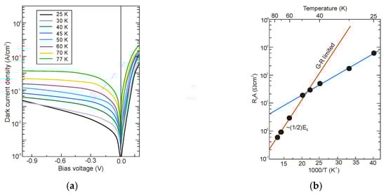
Figure 59.
Dark electrical characteristics of LWIR InAs/InAsSb SL photodiodes: (a) current-voltage characteristics versus temperatures; (b) RoA versus temperature (after [164]).
The spectral characteristics of photodiode are presented in Figure 60. At 77 K, the sample exhibited a 100% λcut-off = 17 µm and 50% λcut-off = 14.6 µm. High QE is reached when biased >150 mV and saturates at 300 mV where the peak current responsivity reaches 4.8 A/W, corresponding to a QE of 46% for a 2.3 µm thick absorber. Detectivity shown in Figure 60b, limited by shot noise and Johnson noise, is estimated using equation
where Ri is the device responsivity.

Figure 60.
Spectral characteristics of LWIR T2SLs InAs/InAsSb photodiode: (a) QE spectrum with different applied bias at 77 K. Inset: 50% λcut-off versus temperature; (b) the calculated shot noise and Johnson noise limited D* at 77K for different applied bias (after [164]).
The effective passivation of T2SLs InAs/InAsSb photodiodes is in a very early stage of development. Usually, photodiodes are not passivated. The simplest passivation is based on the common dielectric insulators deposited onto exposed surface of the device, utilized in the silicon industry (such as an oxide or nitride of silicon). In the case of T2SLs InAs/InAsSb photodiodes, the passivation challenges are caused by the well-known surface accumulation of InAsSb. Sulphur anodic was found to be more effective passivant for p+Bpnn+ detector structure compared to fluoride and chloride anodic films [186]. In [187] the dark current suppression was observed in 8-μm λcut-off T2SLs InAs/InAsSb structure with combination of a double-electron barrier and SiO2 passivation. In addition, the effect of hydrogenation could be taken into account for passivation of bulk defects in MWIR T2SLs InAs/InAsSb [188].
6.2.2. Barrier Detectors
Klipstein et al. [189] proposed the division of the barrier detectors into two groups: XBnn and XBpp, where X is a contact layer where doping, material, or both can be varied. Usually, however, the most popular are four types of SLs barrier detectors schematically described in Table 5.
Table 5.
T2SLs barrier detectors.
Main activity in development of the T2SLs InAs/InAsSb barrier detectors is directed to nBn devices operating in MWIR spectral range at much higher temperatures than InSb photodiodes. Generally, however, these detectors can be optimized for wider spectral range up to VLWIR [191]. The unipolar hole barriers are only available for T2SLs InAs/GaSb and mostly for LWIR. In addition, there is no good hole barrier for T2SLs InAs/InAsSb. Figure 61 shows same images taken with JPL T2SLs arrays in wide IR spectral range. In this section the representative examples of barrier detector performance are presented.
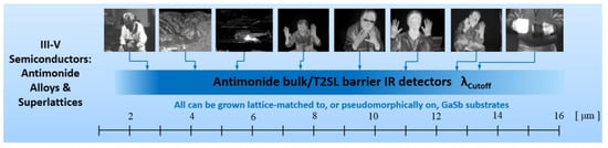
Figure 61.
Images from JPL antimonide bulk and T2SLs barrier FPAs with λcut-off in wide IR range (after [159]).
The JPL nBn device structure grown by MBE on GaSb substrate is similar to that shown in Figure 47a. The top/bottom contacts and active layers consist of 16/20 and 525 periods of (37Å, 13Å) T2SLs InAs/InAs0.66Sb0.34, respectively. As a unipolar barrier located between the top contact and absorber, 120-nm thick AlAs0.085Sb0.915 Be-doped to 1015 cm−3 is used. The top contact and active layers are n.i.d, while the bottom contact is Te-doped to 1017 cm−3.
The experimentally measured dark current density versus applied voltage for temperature range between 89 K and 222 K is shown in Figure 62. The inset shows an Arrhenius plot of dark current under bias −0.2 V with activation energy of 0.205 eV. The dark current density at 157 K and bias voltage of −0.2 V is 9.6 × 10⁻⁵ A/cm2, which is ~4.5 higher than “Rule 07” for λcut-off = 5.4 μm.
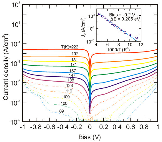
Figure 62.
Dark current density versus voltage, for temperatures 89–222 K. The inset presents the dark current temperature dependence −0.2 V (after [171]).
The QE shown in Figure 63 is derived from measured responsivity of the BSI samples through the GaSb substrate. The QE increases within the range 77–175 K (probably due to reduced hole mobility), and next decreases in the higher temperature (probably due to influence of interfacial detects at the barrier/absorber interface). The insert in the figure for λcut-off = 3.4 μm shows that a low reverse voltage is sufficient to reach maximum responsivity, where hB AlAsSb doping influence on the value of nonzero turn-on voltage is visible.
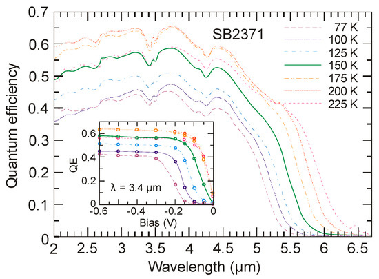
Figure 63.
BSI spectral QE for MWIR detector for temperatures ranging from 77 to 225 K. The inset shows the QE measured at 3.4 µm versus voltage at the same set of temperatures [171].
The MWIR T2SLs InAs/InAsSb nBn detector operating in HOT conditions has demonstrated significant advantages over InSb. It is presented in Figure 64, where the 300 K background limited detectivity versus detector temperature for f/2 optics and 2π field of view (FOV) is shown. The assessed BLIP temperatures are 152 K and 181 K for f/2 and 2π FOV, respectively. In this way, this barrier detector combines the higher operating temperature (comparable with HgCdTe) with the material robustness of InSb. However, for low-background applications, the T2SLs InAs/InAsSb barrier detector still has disadvantages compared to HgCdTe-higher G-R dark current due to shorter SRH lifetimes [171].
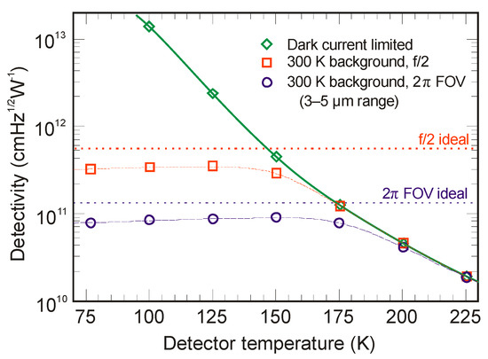
Figure 64.
300 K background, 3–5 µm blackbody detectivity versus temperature for f/2 optics and 2π FOV (dashed lines); the corresponding ideal D* values are indicated by dotted lines. The shot noise limited D* is also depicted (solid line) (after [171]).
Hood et al. [192] modified the barrier structure to present better in performance pBn T2SLs InAs/GaSb LWIR device. In the proposed architecture, the p-n junction can be located at the interface between the heavily doped p-type contact and the low doped barrier or within the low doped barrier itself. Similarly to the nBn, the pBn architecture reduces G-R currents related to the SRH centers (the depletion region is moved to the barrier-no depletion in the low bandgap n-type absorber). In addition, the electric field dropping in the barrier increases the response time which is related to the carriers sweeping from the active layer. Recently, the design, growth, and characterization of the first MWIR T2SLs InAs/InAsSb pBn barrier photodetectors for HOT condition have been demonstrated [176,193].
In the last several years the idea of barrier detectors has been extended to short wavelength infrared wavelength (SWIR) region using InGaAs and InGaAsSb alloy systems [107,194,195,196]. The MBE technology is used as a standard growth method for SWIR detectors fabrication.
Savich et al. [195] carried out a comparison of electrical and optical performance of the typical photodiodes and nBn detectors with λcut-off = 2.8 μm fabricated with both lattice-mismatched InGaAs and lattice-matched InGaAsSb active layers. In order to minimize the number of defects in the InGaAs active layer grown on InP substrate, a 2 μm AlInAs step-graded buffer was grown where the lattice constant was graded from that of InP to that of In0.82Ga0.18As. Both the typical photodiode and nBn detector include this step-graded buffer. The extra pseudomorphic AlAsSb unipolar barrier is added to maintain a high barrier in conduction band in comparison to In0.82Ga0.18As.
In the case of lattice-matched to GaSb, the quaternary composition of In0.30Ga0.70As0.56Sb0.44 at the edge of the miscibility gap was used to maintain the λcut-off and lattice-matching requirements. In nBn detector, also pseudomorphic AlGaSb unipolar barrier with a large CBO and zero VBO in comparison to the In0.30Ga0.70As0.56Sb0.44 absorber was implemented.
Figure 65 shows temperature dependent dark current characteristics for both lattice-mismatched InGaAs and lattice-matched InGaAsSb detectors under reverse bias 100 mV [195]. InGaAs on InP materials exhibit low material quality, i.e., threading dislocations occurring due to the lattice mismatch increasing dark current.
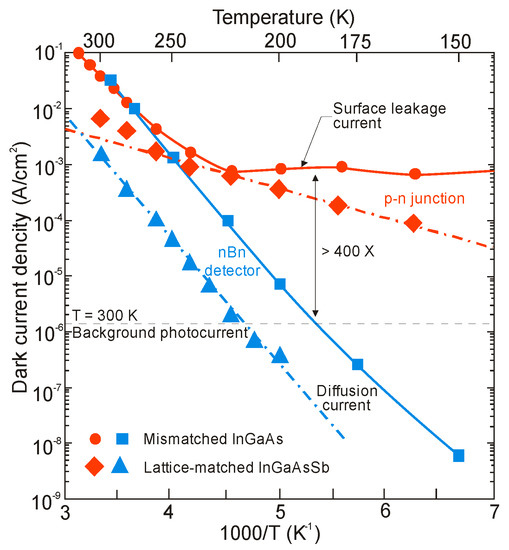
Figure 65.
Arrhenius plots for both InGaAs and InGaAsSb p-n junctions and nBn detectors with λcut-off =2.8 µm (adapted after [195]).
The p-n InGaAs photodiode is limited by surface leakage current for T < 220 K, while the nBn detector remains diffusion limited down to 150 K. At the room temperature background photocurrent level, the nBn detector’s dark current is reduced by 400× in comparison to the typical photodiode.
The p-n InGaAsSb device is limited by depletion region current for T < 250 K, while the nBn remains diffusion limited down to 250 K. At the 300 K background photocurrent level of the nBn, dark current is suppressed by nearly three orders of magnitude in comparison to the typical photodiode.
Figure 66 shows that InGaAsSb nBn detector being lattice-matched to a GaSb substrate presents performance near “Rule 07” where dark current is 10 to 20 times lower in comparison to the lattice-mismatched InGaAs counterpart.
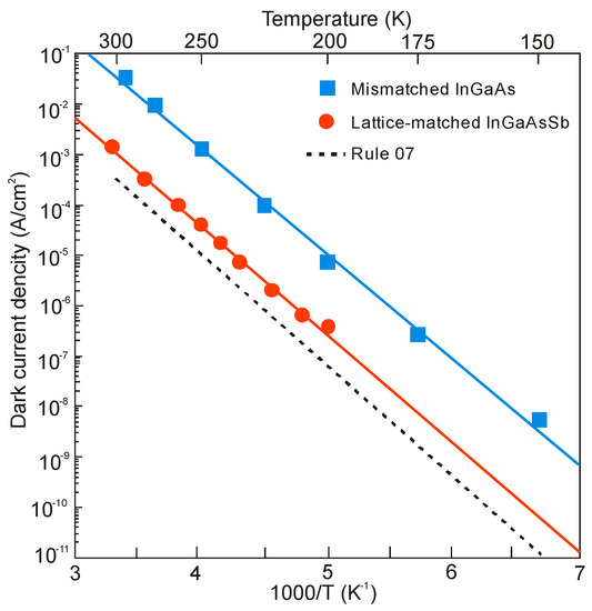
Figure 66.
InGaAs and InGaAsSb nBn dark current comparison. The lattice matched InGaAsSb barrier detector exhibits at least an order of magnitude reduction in the dark current in comparison to the mismatched InGaAs nBn detector (after [195]).
Figure 67 and Figure 68 compare dark currents of different types of barrier and p-i-n detectors constructed on the basis of InAs/GaSb and Ga-free InAs/InAsSb SLs, respectively. Experimental data collected from the literature [107,143,147,155,161,163,173,181,196,197,198,199,200,201,202] is referred to the “Rule 07”. The dark currents of the InAs/GaSb SL detectors differ more from “Rule 07” than the data for Ga-free SL detectors. The best results were achieved by the pMp and the CBIRD detectors, both operating at 77 K. Fabricated by VIGO System Ga-free InAs/InAsSb SLs pBnN detector reaches dark currents measured at high temperatures (210 K and 230 K) in accordance with the “Rule 07” -see Figure 68. Similar results were reached by the detector described in the work of Kim et al. [163] but operating in 77 K. This figure also shows the advantage of barrier detectors over P-i-N devices.
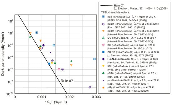
Figure 67.
Comparison of various types InAs/GaSb SL detectors with the “Rule 07”.
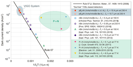
Figure 68.
Comparison of various types Ga-free InAs/InAsSb SL detectors with the “Rule 07”.
6.2.3. Multicolor Detectors
Apart from HgCdTe photodiodes and quantum well infrared photodetectors (QWIPs), T2SLs have emerged as a candidate suitable for multispectral detection due to flexibility in bandgap tuning assuming lattice-matching requirements [203]. The single multicolor detector cell is built of the group of detectors being sensitive to a given spectral band (see Figure 69). The radiation goes through the SWIR detector, while the MWIR/LWIR passes freely to the next detector. The constituent layers absorb IR up to its λcut-off being transparent to the longer wavelengths collected in subsequent layers. The detector structure is fabricated by proper order: MWIR/LWIR optically behind SWIR detector. The operating IR range is addressed by changing the polarity of the voltage.
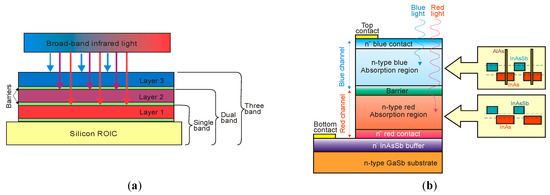
Figure 69.
Multicolor detector cell: (a) architecture of a three-band photodetector. The very first IR band is absorbed in layer 3, while longer wavelength is transmitted through to the next constituent layers. The active layers are separated by thin barriers. (b) SWIR/MWIR dual-band nBn T2SLs InAs/InAsSb back-to-back p-i-n-n-i-p structure and schematic band alignment of SLs building active layers (dotted lines represent the effective bandgaps of SLs) (after [168]).
Northwestern University presented different types of bias-switchable dual-band nBn T2SLs InAs/InAsSb detectors to include MWIR/LWIR and LWIR1/LWIR2 ranges [166,168,204]. The fabrication of dual-band photodetectors is challenging to grow proper electron barrier and SLs designs for both absorption regions with zero VB discontinuity.
Figure 69b presents schematic diagram of a bias-selectable nBn dual-band IR detector based on T2SL InAs/InAsSb/AlAsSb structure together with band alignment of the SLs in two absorption layers. The SLs design of the red absorption region, with nominal λcut-off ~12 μm at 77 K, consists of 30/10 MLs of T2SLs InAs/InAs0.48Sb0.52, respectively. The SLs design of the blue absorption region, with a nominal λcut-off ~8 μm at 77 K, consists of 13/1.5/13/9 MLs of T2SLs InAs/AlAs/InAs/InAs0.48Sb0.52, respectively. The SLs blue channel absorption region contains extra AlAs layer providing the necessary flexibility in the band structure design. The AlAs layer compensates the excessive tensile strain generated by the InAsSb layer in the SLs. The electron barrier is made of 4/3/4/3/4/9 MLs of T2SLs InAs/AlAs0.55Sb0.45/InAs/AlAs0.45Sb0.55/InAs/InAs0.45Sb0.55 with a nominal λcut-off ~4 μm at 77 K. This barrier design provides more flexibility to accommodate the lattice strain.
The two active regions are selected by changing the voltage polarity. The optical performance of the detector is shown in Figure 70a. The blue and red channels exhibit 100% λcut-off ~8.6 μm (~145 meV) and ~12.5 μm (~100 meV) at 77 K, respectively. The blue channel QE saturates at the level of 65% at 6.45 μm and the red channel reaches 50% at 9 μm.

Figure 70.
Performance characteristics of bias-selectable dual-band nBn InAs/InAsSb SL detector at 77 K: (a) spectral QE in FSI configuration without any anti-reflection coating for two applied bias: + 40 mV (blue channel) and −100 mV (red channel), (b) dark current density versus voltage for blue and red channels, (c) D* of the blue and red channels at +40 and −100 mV voltage (after [168]).
Figure 70b shows the dark current density of the dual-band LWIR1/LWIR2 photodetector measured when covered by a 77K cold-shield. At +40 mV, dark current density for the blue channel reaches 1.13 × 10⁻⁶ A/cm2 and detectivity reaches 5.1 × 10¹² cmHz1/2/W at 77 K. The red channel exhibits dark current density at the level of 1.7 × 10⁻⁴ A/cm2 at −100 mV and detectivity of 4.5 × 10¹¹ cmHz1/2/W. The detectivity is estimated using Equation (15).
The results presented here indicate that the T2SLs InAs/InAsSb have the potential for multispectral IR imagers and can be a possible alternative for current state-of-the-art T2SLs InAs/GaSb.
7. InAsSb-based Superlattice Focal Plane Arrays
The noise equivalent difference temperature (NEDT) is a figure of merit for thermal imagers giving information on the detector array sensitivity and can be expressed according to the relations [3,78].
where ΦB—background flux, τint—integration time, Nw-well capacity of readout, JΦ = ηΦBA—background flux current. The overall QE of the detector, including the internal QE is given by η. The cold shield efficiency and optics transmission are taken to be unity.
Assuming that the scene contrast, C = (dΦB/dT)/ΦB, NEDT can be rewritten:
The calculated C for MWIR and LWIR is 3.5–4% and 1.7% at 300 K, respectively. Well capacity for a 15-μm pixel stays within the range Nw = 1 × 10⁶ to 1 × 10⁷ electrons. Equation (18) indicates that if the Idark/IΦ ratio increases and/or QE decreases, the longer integration time and the faster optics have to be implemented.
Figure 71 presents NEDT versus temperature for barrier detectors and HgCdTe photodiodes with λcut-off = 5 μm and 10 μm. The theoretical HgCdTe photodiodes performance limit is higher than for barrier detectors for T > 150 K in a MWIR and T > 80 K in a LWIR range. However, taking into account both types of T2SLs, the operating temperature of InAs/InAsSb based detector is higher. For low temperatures the figure of merit of both T2SLs allows for similar performance to be reached, being mainly limited by the readout circuits.

Figure 71.
NEDT versus temperature for barrier detectors and HgCdTe photodiodes for λcut-off = 5 µm (a) and 10 µm (b).
7.1. InAsSb nBn Detector FPAs
The MWIR InAsSb nBn arrays are fabricated by several companies. The nBn cell is considered to be self-passivating design, decreasing leakage current and improving reliability and manufacturability. The simple design (see Table 5) is a major advantage in the large IR FPA state of the art.
First nBn InAsSb array commercially developed by Lockheed Martin Santa Barbara Focalplane operates within the temperature range T = 145–175 K. The 12 μm pixel-pitch MWIR nBn sensor of the 1280 × 1024 format is packaged in a 1.4” diameter dewar with net housing length ~3.8” to include the cooler. That cooler and electronics are reported to consume 5 W and guarantees 25k hours of operation [205].
Klipstein et al. demonstrated nBn array operating in the MWIR (3.4–4.2 μm) at T = 150 K, with f/5.5 optics developed by SCD known as “Kinglet” [206]. The 640 × 512 “Kinglet” is based on SCD’s Pelican-D readout integrated circuit (ROIC) and 15-μm pitch InAs0.91Sb0.09/B-AlAsSb architecture. The NEDT for f/3.2 optics and the pixel operability versus temperature is presented in Figure 72, reaching 20 mK at τint = 10 ms and the pixel operability after a typical two point nonuniformity correction is higher than 99.5%, respectively. The NEDT and operability change sharply for T > 170 K, being consistent with the BLIP temperature of 175 K.
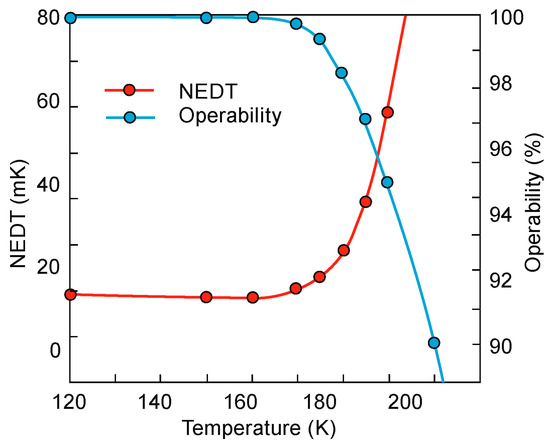
Figure 72.
“Kinglet” NEDT and pixel operability temperature dependence for f/3.2 optics (after [206]).
Recently, SCD has presented several 10 μm pitch nBn 1920 × 1536, 1280 × 1024 and 640 × 512 arrays, integrated with the Blackbird ROICs designed for HOT conditions [207]. Table 6 summarizes the performance of two InAsSb barrier devices fabricated by IR Cameras and SCD. In comparison with standard InSb photodiode arrays, the integrated detector cooler assembles (IDCAs) of nBn devices are characterized by SWaP advantages. For 15-µm pitch 1280 × 1024 FPA, the IDCA weight is reduced by 10%, the power consumption by 70%, and the mean time to failure (MTTF) is increased by more than 100%. Figure 73 presents an image reached by a HOT Hercules array at 150 K [208]. The very first demonstration of the 5 µm pixels 2040 × 1156 was reported in [209].
Table 6.
nBn InAsSb FPA characteristics.

Figure 73.
Image taken by 15 µm HOT Hercules 1280 × 1024, InAs0.91Sb0.09 XBn FPA at f/3 optics, and 150 K (after [208]).
7.2. InAs/InAsSb Superlattice Detector FPAs
T2SLs are especially helpful for fabrication of barrier detectors due to almost perfect control of band edge alignments. Their compatibility with conventional p-n photodiode architecture gives further enhancement in performance improvement. As was first shown by Savich at el. [210], depending on the barrier placement, different dark current components are filtered.
JPL demonstrated extended SWIR (e-SWIR), MWIR, and LWIR images taken with Sb-based FPAs. Whereas the e- SWIR detector is based on a bulk InGaAsSb absorber, the T2SLs InAs/InAsSb active layers were used for MWIR and LWIR. Table 7 presents high-performance, cost-effective 640 × 512 FPAs for MWIR and LWIR ranges. HOT nBn photodetectors operate at 150 K covering the near infrared (NIR, 0.75–1.4 µm), SWIR (1.4–3 µm), and MWIR atmospheric transmission window (3–5 µm) with very high QE. Figure 74 shows 640 × 512 FPAs images taken in different spectral ranges.
Table 7.
Performance of InAs/InAsSb T2SLs nBn detector FPAs ([172,211]).
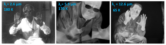
Figure 74.
e-SWIR, MIWR, and LWIR images registered by Sb-based FPA. The e-SWIR FPA is based on a bulk InGaAsSb, T2SLs InAs/InAsSb active layer was used for the MWIR and LWIR (after [107]).
Figure 75 shows the performance of the 24 μm pitch 640 × 512 FPA with λcut-off ~5.4 μm (see Table 7) and direct injection (DI) ROIC with Nw = 8 × 10⁶ electrons. NEDT is below 19 mK for T < 160 K, and increases up to ~55 mK at 180 K. The operability is 99.7% up to 160 K and decreases to 99.3% at 180 K. NEDT exhibits excellent uniformity with 8 mK distribution [172]. Both NEDT and operability are similar to those described previously for 15 μm pitch nBn InAs0.91Sb0.09/B-AlAsSb 640 × 512 FPA shown in Figure 72.
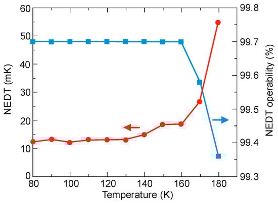
Figure 75.
NEDT and operability versus temperature for 24 µm pitch MWIR 640 × 512 nBn InAs/InAsSb FPA.
The LWIR barrier structures have also shown significant improvement in operating temperature in comparison to the typical p-n designs. Figure 76 presents the dark current density and the QE versus temperature for LWIR square mesa T2SLs InAs/InAsSb barrier detectors (area 250 × 250 µm2) [212]. The devices were grown on a 4”, Te-doped GaSb (100) substrate by MBE. The −50 mV dark current density at 70 K is 4 × 10⁻⁵ A/cm2. The QE derived from BSI (through the GaSb substrate) responsivity measurements has not been corrected for substrate reflection or transmission.
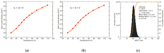
Figure 76.
The LWIR (λcut-off = 11 µm at 60 K) nBn T2SLs InAs/InAsSb photodetectors performance: (a) dark current density versus temperature for −0.1 V, (b) BSI QE (no AR coating) measured for T = 60–75 K, (c) NEDT for 640 × 512 FPA for T = 60 K, 300 K blackbody temperature and f/4 cold stop (after [212]).
The LWIR detector was used to fabricate 24 µm pitch, 640 × 512 FPA and Lockheed Martin SBF-193 ROIC. The measured 640 × 512 FPA NEDT histogram for T = 60 K, 300 K blackbody temperature and f/4 cold stop is shown in Figure 76c. The 21 mK NEDT is in fair agreement with the estimated NEDT based on a single element test detector data [212].
8. Conclusions
There are many critical challenges for future civilian and military IR detector applications. The main efforts are directed to decrease IR imaging systems SWaP by increasing the FPA’s operating temperature. Nowadays, HgCdTe is the most common material for IR photodetectors being the reference for alternative technologies to include uncooled operation. After sixty years of development, HgCdTe has just reached ultimate HOT performance limit estimated by “Law 19”-the ultimate photodiode performance metric [117]. This metric has been recently supported by experimental data of fully-depleted HgCdTe P-i-N photodiodes. The “Law 19” corresponds exactly the BLIP for room temperature operation.
The InAsSb-based IR photodetectors’ performance is comparable with HgCdTe:
- III-V compounds exhibit inherently short SRH lifetimes typically below 1 μs requiring the nBn design to operate at higher temperatures (this applies both to the bulk InAsSb and the T2SLs),
- T2SLs InAs/InAsSb has emerged in recent years as an alternative to the T2SLs InAs/GaSb due to the three reasons: (i) a better growth controllability and simpler manufacturability, (ii) longer SRH lifetimes (10 μs in MWIR SLs in comparison with 400 ns for InSb), and (iii) significantly higher operating temperature than InSb,
- HgCdTe exhibits long SRH lifetimes >200 μs to 50 ms depending on the λcut-off [78] (can operate with either architecture and may be diffusion or depletion current limited),
- III-Vs exhibit comparable performance to HgCdTe for equivalent λcut-off, but for lower temperature, due to the inherent difference in SRH lifetimes,
- III-V materials are more robust than their II-VI counterparts due to stronger (less ionic) chemical bonding what allows to reach better operability, spatial uniformity, temporal stability, scalability, producibility, and affordability-the so-called “ibility” advantages.
Table 8 gathers the LWIR detectors state of the art fabricated from selected materials. The highest level of maturity (technology readiness level, TRL = 9) is credited to HgCdTe photodiodes, microbolometers, and for QWIPs. The T2SLs InAs/InAsSb structures have proven the potential for MWIR and LWIR applications with performance comparable to HgCdTe for the same λcut-off. Strong progress toward mature SLs and barrier detector technologies, including their commercialization, has been observed in the last decade. It is expected that InAsSb-based materials strengthen dominant position of InSb especially in MWIR FPA market in volume due to “ibility” advantages of III-V semiconductors. HgCdTe detectors allow one to reach lower dark current and HOT conditions and are/will be a material of choice for more demanding applications.
Table 8.
LWIR device state-of-the-art. TRL-technology readiness level (TRL = 10 ideal maturity).
Author Contributions
Conceptualization, A.R., P.M. (Piotr Martyniuk); writing—original draft preparation, A.R., P.M. (Piotr Martyniuk), M.K., P.M. (Pawel Madejczyk), S.K.; writing—review and editing, A.R., P.M. (Piotr Martyniuk), M.K.; visualization, A.R., P.M. (Piotr Martyniuk), M.K.; supervision, A.R., P.M. (Piotr Martyniuk); project administration, A.R., P.M. (Piotr Martyniuk), M.K., P.M. (Pawel Madejczyk); funding acquisition, A.R., P.M. (Piotr Martyniuk), M.K., P.M. (Pawel Madejczyk). All authors have read and agreed to the published version of the manuscript.
Funding
The writing of the paper has been partially done under financial support of The National Science Centre-Grant nos. UMO-2018/30/M/ST7/00174, UMO-2018/31/B/ST7/01541, and UMO-2019/33/B/ST7/00614 and The National Centre for Research and Development—the grant no. Mazowsze/0090/19-00.
Conflicts of Interest
The authors declare no conflict of interest. The funders had no role in the design of the study; in the collection, analyses, or interpretation of data; in the writing of the manuscript, or in the decision to publish the results.
References
- Woolley, J.C.; Smith, B.A. Solid Solution in AIIIBVCompounds. Proc. Phys. Soc. 1958, 72, 214–223. [Google Scholar] [CrossRef]
- Lawson, W.; Nielsen, S.; Putley, E.; Young, A. Preparation and properties of HgTe and mixed crystals of HgTe-CdTe. J. Phys. Chem. Solids 1959, 9, 325–329. [Google Scholar] [CrossRef]
- Rogalski, A. Infrared and Terahertz Detectors, 3rd ed.; CRC Press: Boca Raton, FL, USA, 2019. [Google Scholar]
- Elliott, T. Recollections of MCT work in the UK at Malvern and Southampton. In Proceedings of the SPIE Defense, Security, and Sensing, Orlando, FL, USA, 13–17 April 2009. [Google Scholar]
- Melngailis, I.; Harman, T. Chapter 4 Single-Crystal Lead-Tin Chalcogenides; Elsevier BV: Amsterdam, The Netherlands, 1970; Volume 5, pp. 111–174. [Google Scholar]
- Harman, T.; Melngailis, I. Narrow Gap Semiconductors. In Applied Solid State Science; Elsevier BV: Amsterdam, The Netherlands, 1974; Volume 4, pp. 1–94. [Google Scholar]
- Rogalski, A.; Piotrowski, J. Intrinsic infrared detectors. Prog. Quantum Electron. 1988, 12, 87–289. [Google Scholar] [CrossRef]
- Cheung, D.T.; Andrews, A.M.; Gertner, E.R.; Williams, G.M.; Clarke, J.E.; Pasko, J.G.; Longo, J.T. Backside-illuminated InAs1−xSbx-InAs narrow-band photodetectors. Appl. Phys. Lett. 1977, 30, 587–589. [Google Scholar] [CrossRef]
- Bubulac, L.O.; Andrews, A.M.; Gertner, E.R.; Cheung, D.T. Backside-illuminated InAsSb/GaSb broadband detectors. Appl. Phys. Lett. 1980, 36, 734. [Google Scholar] [CrossRef]
- Schulman, J.N.; McGill, T.C. The CdTe/HgTe superlattice: Proposal for a new infrared material. Appl. Phys. Lett. 1979, 34, 663–665. [Google Scholar] [CrossRef]
- Osbourn, G.C. InAsSb strained-layer superlattices for long wavelength detector applications. J. Vac. Sci. Technol. B Microelectron. Nanometer Struct. 1984, 2, 176. [Google Scholar] [CrossRef]
- Smith, D.L.; Mailhiot, C. Proposal for strained type II superlattice infrared detectors. J. Appl. Phys. 1987, 62, 2545–2548. [Google Scholar] [CrossRef]
- Mailhiot, C. Long-wavelength infrared detectors based on strained InAs–Ga1−xInxSb type-II superlattices. J. Vac. Sci. Technol. A 1989, 7, 445–449. [Google Scholar] [CrossRef]
- Chow, D.H.; Miles, R.H.; Söderström, J.R.; McGill, T.C. Growth and characterization of InAs/Ga1−xInxSb strained-layer superlattices. Appl. Phys. Lett. 1990, 56, 1418–1420. [Google Scholar] [CrossRef]
- Kurtz, S.; Dawson, L.; Zipperian, T.; Whaley, R. High-detectivity (>1 × 1010 cm Hz½/W), InAsSb strained-layer superlattice, photovoltaic infrared detector. IEEE Electron Device Lett. 1990, 11, 54–56. [Google Scholar] [CrossRef]
- Chadda, S.; Datye, A.K.; Dawson, L.R. Microstructural evaluation of strained multilayer InAsSb/InSb infrared detectors by transmission electron microscopy. J. Appl. Phys. 1993, 73, 4232–4239. [Google Scholar] [CrossRef]
- Lackner, D.; Pitts, O.J.; Steger, M.; Yang, A.; Thewalt, M.L.W.; Watkins, S.P. Strain balanced InAs/InAsSb superlattice structures with optical emission to 10 μm. Appl. Phys. Lett. 2009, 95, 81906. [Google Scholar] [CrossRef]
- Steenbergen, E.H.; Connelly, B.C.; Metcalfe, G.D.; Shen, H.; Wraback, M.; Lubyshev, D.I.; Qiu, Y.; Fastenau, J.M.; Liu, A.W.K.; Elhamri, S.; et al. Significantly improved minority carrier lifetime observed in a long-wavelength infrared III-V type-II superlattice comprised of InAs/InAsSb. Appl. Phys. Lett. 2011, 99, 251110. [Google Scholar] [CrossRef]
- Rogalski, A. InAs1−xSbx infrared detectors. Prog. Quantum Electron. 1989, 13, 191–231. [Google Scholar] [CrossRef]
- Steenbergen, E.H. InAsSb-Based Photodetectors; Elsevier BV: Amsterdam, The Netherlands, 2020; pp. 415–453. [Google Scholar]
- Rogalski, A. New Ternary Alloy Systems for Infrared Detectors; SPIE: Zakopane, Poland, 1993; pp. 52–60. [Google Scholar]
- Woolley, J.C.; Warner, J. Optical energy-gap variation in InAs–InSb alloys. Can. J. Phys. 1964, 42, 1879–1885. [Google Scholar] [CrossRef]
- Coderre, W.M.; Woolley, J.C. Electrical properties of InAsxSb1−x alloys. Can. J. Phys. 1968, 46, 1207–1214. [Google Scholar] [CrossRef]
- Woolley, J.C.; Thompson, A.G. Calculation of electron effective mass in iii-v alloys. Can. J. Phys. 1964, 42, 2030–2034. [Google Scholar] [CrossRef]
- Aubin, M.J.; Woolley, J.C. Electron scattering in InAsxSb1−x alloys. Can. J. Phys. 1968, 46, 1191–1198. [Google Scholar] [CrossRef]
- Van Tongerloo, E.H.; Woolley, J.C. Free-carrier Faraday rotation in InAsxSb1−x alloys. Can. J. Phys. 1968, 46, 1199–1206. [Google Scholar] [CrossRef]
- Springer. Springer Handbook of Electronic and Photonic Materials, 2nd ed.; Kasap, S., Capper, P., Eds.; Springer International Publishing: New York, NY, USA, 2017. [Google Scholar]
- Pelzel, R. A comparison of MOVPE and MBE growth technologies for III-V epitaxial structures. In Proceedings of the CS MANTECH Conference, New Orleans, LA, USA, 13–16 May 2013; pp. 105–108. [Google Scholar]
- Manasevit, H. The use of metalorganics in the preparation of semiconductor materials: Growth on insulating substrates. J. Cryst. Growth 1972, 13, 306–314. [Google Scholar] [CrossRef]
- Biefeld, R.M. The metal-organic chemical vapor deposition and properties of III–V antimony-based semiconductor materials. Mater. Sci. Eng. R Rep. 2002, 36, 105–142. [Google Scholar] [CrossRef]
- Wang, C. Progress and continuing challenges in GaSb-based III–V alloys and heterostructures grown by organometallic vapor-phase epitaxy. J. Cryst. Growth 2004, 272, 664–681. [Google Scholar] [CrossRef]
- Chang, C.-A.; Ludeke, R.; Chang, L.L.; Esaki, L. Molecular-beam epitaxy (MBE) of In1−xGaxAs and GaSb1−yAsy. Appl. Phys. Lett. 1977, 31, 759–761. [Google Scholar] [CrossRef]
- Ludeke, R. Electronic Properties of (100) Surfaces of GaSb and InAs and Their Alloys with GaAs. IBM J. Res. Dev. 1978, 22, 304–314. [Google Scholar] [CrossRef]
- Bennett, B.R.; Shanabrook, B.V.; Liu, W.K.; Santos, M.B. Molecular Beam Epitaxy of Sb-based Semiconductors. In Series on Directions in Condensed Matter Physics; World Scientific Publishing Co Pte Lt: Singapore, 1999; pp. 401–452. [Google Scholar]
- Mauk, M.G.; Andreev, V.M. GaSb-related materials for TPV cells. Semicond. Sci. Technol. 2003, 18, S191–S201. [Google Scholar] [CrossRef]
- Zhang, Y.-H. Accurate control of As and Sb incorporation ratio during solid-source molecular-beam epitaxy. J. Cryst. Growth 1995, 150, 838–843. [Google Scholar] [CrossRef]
- Lew, A.Y. Atomic-scale structure of InAs/InAs1−xSbx superlattices grown by modulated molecular beam epitaxy. J. Vac. Sci. Technol. B Microelectron. Nanometer Struct. 1996, 14, 29–40. [Google Scholar] [CrossRef]
- Zhang, Y.H.; Lew, A.; Yu, E.; Chen, Y. Microstructural properties of superlattices and InAsxSb1−x ordered alloys grown by modulated molecular beam epitaxy. J. Cryst. Growth 1997, 833–837. [Google Scholar] [CrossRef]
- Svensson, S.P.; Sarney, W.L.; Hier, H.; Lin, Y.; Wang, D.; Donetsky, D.; Shterengas, L.; Kipshidze, G.; Belenky, G. Band gap of InAs1−xSbx with native lattice constant. Phys. Rev. B 2012, 86. [Google Scholar] [CrossRef]
- Winkler, G.W.; Wu, Q.; Troyer, M.; Krogstrup, P.; Soluyanov, A.A. Topological Phases in InAs1−xSbx: From Novel Topological Semimetal to Majorana Wire. Phys. Rev. Lett. 2016, 117, 76–403. [Google Scholar] [CrossRef] [PubMed]
- Belenky, G.; Donetsky, D.; Kipshidze, G.; Wang, D.; Shterengas, L.; Sarney, W.L.; Svensson, S.P. Properties of unrelaxed InAs1−xSbx alloys grown on compositionally graded buffers. Appl. Phys. Lett. 2011, 99, 141116. [Google Scholar] [CrossRef]
- Lin, Y.; Donetsky, D.; Wang, D.; Westerfeld, D.; Kipshidze, G.; Shterengas, L.; Sarney, W.L.; Svensson, S.P.; Belenky, G. Development of Bulk InAsSb Alloys and Barrier Heterostructures for Long-Wave Infrared Detectors. J. Electron. Mater. 2015, 44, 3360–3366. [Google Scholar] [CrossRef]
- Varshni, Y. Temperature dependence of the energy gap in semiconductors. Physica 1967, 34, 149–154. [Google Scholar] [CrossRef]
- Viña, L.; Logothetidis, S.; Cardona, M. Temperature dependence of the dielectric function of germanium. Phys. Rev. B 1984, 30, 1979–1991. [Google Scholar] [CrossRef]
- Fan, H.Y. Temperature Dependence of the Energy Gap in Semiconductors. Phys. Rev. 1951, 82, 900–905. [Google Scholar] [CrossRef]
- Wieder, H.; Clawson, A. Photo-electronic properties of InAs0.07Sb0.93films. Thin Solid Films 1973, 15, 217–221. [Google Scholar] [CrossRef]
- Murawski, K.; Gomółka, E.; Kopytko, M.; Grodecki, K.; Michalczewski, K.; Kubiszyn, Ł.; Gawron, W.; Martyniuk, P.; Rogalski, A.; Piotrowski, J. Bandgap energy determination of InAsSb epilayers grown by molecular beam epitaxy on GaAs substrates. Prog. Nat. Sci. 2019, 29, 472–476. [Google Scholar] [CrossRef]
- Thompson, A.G.; Woolley, J.C. Energy-gap variation in mixed III-V alloys. Can. J. Phys. 1967, 45, 255–261. [Google Scholar] [CrossRef]
- Webster, P.T.; Riordan, N.A.; Liu, S.; Steenbergen, E.H.; Synowicki, R.A.; Zhang, Y.-H.; Johnson, S.R. Measurement of InAsSb bandgap energy and InAs/InAsSb band edge positions using spectroscopic ellipsometry and photoluminescence spectroscopy. J. Appl. Phys. 2015, 118, 245–706. [Google Scholar] [CrossRef]
- Vurgaftman, I.; Meyer, J.R.; Ram-Mohan, L.R. Band parameters for III–V compound semiconductors and their alloys. J. Appl. Phys. 2001, 89, 5815–5875. [Google Scholar] [CrossRef]
- Rogalski, A.; Jóźwikowski, K. Intrinsic carrier concentration and effective masses in InAs1−xSbx. Infrared Phys. 1989, 29, 35–42. [Google Scholar] [CrossRef]
- Tomasulo, S.; Affouda, C.A.; Mahadik, N.A.; Twigg, M.E.; Yakes, M.K.; Aifer, E.H. Sb-incorporation in MBE-grown metamorphic InAsSb for long-wavelength infrared applications. J. Vac. Sci. Technol. B 2018, 36, 02D108. [Google Scholar] [CrossRef]
- Razeghi, M. Overview of antimonide based III-V semiconductor epitaxial layers and their applications at the center for quantum devices. Eur. Phys. J. Appl. Phys. 2003, 23, 149–205. [Google Scholar] [CrossRef]
- Smith, S.N.; Phillips, C.C.; Thomas, R.H.; Stradling, R.A.; Ferguson, I.T.; Norman, A.; Murdin, B.N.; Pidgeon, C. Interband magneto-optics of InAs1−xSbx. Semicond. Sci. Technol. 1992, 7, 900–906. [Google Scholar] [CrossRef]
- Suchalkin, S.; Ludwig, J.; Belenky, G.; Laikhtman, B.; Kipshidze, G.; Lin, Y.; Shterengas, L.; Smirnov, D.; Luryi, S.; Sarney, W.L.; et al. Electronic properties of unstrained unrelaxed narrow gap InAsxSb1−x alloys. J. Phys. D Appl. Phys. 2016, 49, 101–105. [Google Scholar] [CrossRef]
- Fang, Z.M.; Ma, K.Y.; Jaw, D.H.; Cohen, R.M.; Stringfellow, G.B. Photoluminescence of InSb, InAs, and InAsSb grown by organometallic vapor phase epitaxy. J. Appl. Phys. 1990, 67, 7034–7039. [Google Scholar] [CrossRef]
- Kroemer, H. The family (InAs, GaSb, AlSb) and its heterostructures: A selective review. Phys. E Low Dimens. Syst. Nanostruct. 2004, 20, 196–203. [Google Scholar] [CrossRef]
- Steenbergen, E.H.; Cellek, O.O.; Lubyshev, D.; Qiu, Y.; Fastenau, J.M.; Liu, A.W.K.; Zhang, Y.-H. Study of the valence band offsets between InAs and InAs1−xSbx alloys. In Proceedings of the SPIE OPTO, San Francisco, CA, USA, 21–26 January 2012; Volume 82680K. [Google Scholar]
- Kurtz, S.R.; Biefeld, R.M. Magnetophotoluminescence of biaxially compressed InAsSb quantum wells. Appl. Phys. Lett. 1995, 66, 364–366. [Google Scholar] [CrossRef]
- Tang, P.J.P.; Pullin, M.J.; Li, Y.B.; Phillips, C.C.; Stradling, R.A.; Chung, S.J.; Yuen, W.T.; Hart, L.; Bain, D.J.; Galbraith, I. A magneto-photoluminescence investigation of the band offset between InAs and arsenic-rich InAs1−xSbx alloys. Appl. Phys. Lett. 1996, 69, 2501–2503. [Google Scholar] [CrossRef]
- Li, Y.B.; Stradling, R.A.; Norman, A.G.; Tang, P.J.P.; Chung, S.J.; Phillips, C.C. Band offsets for InAs1-xSbx/InAs1-ySby strained layer superlattices derived from interband magneto-optical studies. In Proceedings of the 22nd International Conference on the Physics of Semiconductors, Vancouver, BC, Canada, 15–19 August 1994; pp. 1496–1499. [Google Scholar]
- Zhang, Y. Continuous wave operation of InAs/InAsxSb1−x midinfrared lasers. Appl. Phys. Lett. 1995, 66, 118–120. [Google Scholar] [CrossRef]
- Sarney, W.L.; Svensson, S.P.; Lin, Y.; Donetsky, D.; Shterengas, L.; Kipshidze, G.; Belenky, G. Extremely small bandgaps, engineered by controlled multi-scale ordering in InAsSb. J. Appl. Phys. 2016, 119, 215–704. [Google Scholar] [CrossRef]
- Lin, Y.; Wang, D.; Donetsky, D.; Shterengas, L.; Kipshidze, G.; Belenky, G.; Svensson, S.P.; Sarney, W.L.; Hier, H.S. Conduction- and Valence-Band Energies in Bulk InAs1−xSbx and Type II InAs1−xSbx/InAs Strained-Layer Superlattices. J. Electron. Mater. 2013, 42, 918–926. [Google Scholar] [CrossRef]
- Rogalski, A.; Adamiec, K.; Rutkowski, J. Narrow-Gap Semiconductor Photodiodes; SPIE Press: Bellingham, WA, USA, 2000. [Google Scholar]
- Schoen, J.M. Augmented-Plane-Wave Virtual-Crystal Approximation. Phys. Rev. 1969, 184, 858–863. [Google Scholar] [CrossRef]
- Boucenna, M.; Bouarissa, N. Energy gaps and lattice dynamic properties of InAsxSb1−x. Mater. Sci. Eng. B 2007, 138, 228–234. [Google Scholar] [CrossRef]
- Ben Fredj, A.; Debbichi, M.; Said, M. Influence of the composition fluctuation and the disorder on the bowing band gap in semiconductor materials. Microelectron. J. 2007, 38, 860–870. [Google Scholar] [CrossRef]
- Walpole, J.N. Capacitance-Voltage Characteristics of Metal Barriers on p PbTe and p InAs: Effects of the Inversion Layer. J. Appl. Phys. 1971, 42, 5609. [Google Scholar] [CrossRef]
- Wieder, H.H. Transport coefficients of InAs epilayers. Appl. Phys. Lett. 1974, 25, 206–208. [Google Scholar] [CrossRef]
- Casias, L.K.; Morath, C.P.; Steenbergen, E.H.; Webster, P.T.; Kim, J.K.; Cowan, V.M.; Balakrishnan, G.; Krishna, S. Carrier concentration and transport in Be-doped InAsSb for infrared sensing applications. Infrared Phys. Technol. 2019, 96, 184–191. [Google Scholar] [CrossRef]
- Gao, Y.Z.; Kan, H.; Aoyama, M.; Yamaguchi, T. Germanium- and Zinc-Doped P-type InAsSb Single Crystals with a Cutoff Wavelength of 12.5 µm. Jpn. J. Appl. Phys. 2000, 39, 2520–2522. [Google Scholar] [CrossRef]
- Anderson, W. Absorption constant of Pb1−xSnxTe and Hg1−xCdxTe alloys. Infrared Phys. 1980, 20, 363–372. [Google Scholar] [CrossRef]
- Woolley, J.C.; Warner, J. Preparation of InAs-InSb Alloys. J. Electrochem. Soc. 1964, 111, 1142–1145. [Google Scholar] [CrossRef]
- Van Vechten, J.A.; Berolo, O.; Woolley, J.C. Spin-Orbit Splitting in Compositionally Disordered Semiconductors. Phys. Rev. Lett. 1972, 29, 1400–1403. [Google Scholar] [CrossRef]
- Chin, V.W.L.; Egan, R.; Tansley, T.L. Electron mobility in InAs1−xSbx and the effect of alloy scattering. J. Appl. Phys. 1991, 69, 3571–3577. [Google Scholar] [CrossRef]
- Egan, R.; Chin, V.W.L.; Tansley, T.L. Dislocation scattering effects on electron mobility in InAsSb. J. Appl. Phys. 1994, 75, 2473–2476. [Google Scholar] [CrossRef]
- Kinch, M.A. State-of-the-Art Infrared Detector Technology. In State-of-the-Art Infrared Detector Technology; SPIE Press: Bellingham, WA, USA, 2014. [Google Scholar]
- Blakemore, J. Semiconductor Statistics; Elsevier BV: Amsterdam, The Netherlands, 1962. [Google Scholar]
- Nimtz, G. Recombination in narrow-gap semiconductors. Phys. Rep. 1980, 63, 265–300. [Google Scholar] [CrossRef]
- Landsberg, P.T. Recombination in semiconductors. Nat. Cell Biol. 1978, 275, 270–271. [Google Scholar] [CrossRef]
- Shockley, W.; Read, J.W.T. Statistics of the Recombinations of Holes and Electrons. Phys. Rev. 1952, 87, 835–842. [Google Scholar] [CrossRef]
- Hall, R.N. Electron-Hole Recombination in Germanium. Phys. Rev. 1952, 87, 387. [Google Scholar] [CrossRef]
- Humphreys, R. Radiative lifetime in semiconductors for infrared detection. Infrared Phys. 1986, 26, 337–342. [Google Scholar] [CrossRef]
- Elliott, C.T.; Gordon, N.T.; White, A.M. Towards background-limited, room-temperature, infrared photon detectors in the 3–13 μm wavelength range. Appl. Phys. Lett. 1999, 74, 2881–2883. [Google Scholar] [CrossRef]
- Elliott, C.T.; Jones, C.L. Non-equilibrium devices in HgCdTe. In Narrow-gap II-VI Compounds for Optoelectronic and Electromagnetic Applications; Springer Science and Business Media LLC: Berlin, Germany, 1997; pp. 474–485. [Google Scholar]
- Jóźwikowski, K.; Kopytko, M.; Rogalski, A. Numerical Estimations of Carrier Generation–Recombination Processes and the Photon Recycling Effect in HgCdTe Heterostructure Photodiodes. J. Electron. Mater. 2012, 41, 2766–2774. [Google Scholar] [CrossRef][Green Version]
- Rogalski, A.; Kopytko, M.; Martyniuk, P. Antimonide-based Infrared Detectors: A New Perspective; SPIE Press: Bellingham, WA, USA, 2018. [Google Scholar]
- Cripps, S.; Hosea, T.J.C.; Krier, A.; Smirnov, V.; Batty, P.; Zhuang, Q.; Lin, H.; Liu, P.-W.; Tsai, G. Determination of the fundamental and spin-orbit-splitting band gap energies of InAsSb-based ternary and pentenary alloys using mid-infrared photoreflectance. Thin Solid Films 2008, 516, 8049–8058. [Google Scholar] [CrossRef]
- Rogalski, A.; Orman, Z. Band-to-band recombination in InAs1−xSbx. Infrared Phys. 1985, 25, 551–560. [Google Scholar] [CrossRef]
- Wrobel, J.M.; Ciupa, R.; Rogalski, A. Performance limits of room-temperature InAsSb photodiodes. SPIE Def. Secur. Sens. 2010, 7660. [Google Scholar] [CrossRef]
- Jost, S.R.; Meikleham, V.F.; Myers, T.H. InSb: A Key Material for IR Detector Applications. MRS Proc. 1986, 90, 429–436. [Google Scholar] [CrossRef]
- Dobbelaere, W.; De Boeck, J.; Van Mieghem, P.; Mertens, R.; Borghs, G. Optical characterization of Si-doped InAs1−xSbx grown on GaAs and GaAs-coated Si by molecular-beam epitaxy. J. Appl. Phys. 1991, 69, 2536–2542. [Google Scholar] [CrossRef]
- Chu, J.-H.; Mi, Z.-Y.; Tang, D.-Y. Band-to-band optical absorption in narrow-gap Hg1−xCdxTe semiconductors. J. Appl. Phys. 1992, 71, 3955–3961. [Google Scholar] [CrossRef]
- Chu, J.; Li, B.; Liu, K.; Tang, D. Empirical rule of intrinsic absorption spectroscopy in Hg1−xCdxTe. J. Appl. Phys. 1994, 75, 1234–1235. [Google Scholar] [CrossRef]
- Webster, P.T.; Riordan, N.A.; Liu, S.; Steenbergen, E.H.; Synowicki, R.A.; Zhang, Y.-H.; Johnson, S.R. Absorption properties of type-II InAs/InAsSb superlattices measured by spectroscopic ellipsometry. Appl. Phys. Lett. 2015, 106. [Google Scholar] [CrossRef]
- Cherng, Y.T.; Ma, K.Y.; Stringfellow, G.B. Raman scattering in InAs1−xSbx grown by organometallic vapor phase epitaxy. Appl. Phys. Lett. 1988, 53, 886–887. [Google Scholar] [CrossRef]
- Li, Y.B.; Dosanjh, S.S.; Ferguson, I.T.; Norman, A.G.; De Oliveira, A.G.; A Stradling, R.; Zallen, R. Raman scattering in InAs1−xSbx alloys grown on GaAs by molecular beam epitaxy. Semicond. Sci. Technol. 1992, 7, 567–570. [Google Scholar] [CrossRef]
- Erkuş, M.; Serincan, U. Phonon frequency variations in high quality InAs1−xSbx epilayers grown on GaAs. Appl. Surf. Sci. 2014, 318, 28–31. [Google Scholar] [CrossRef]
- Grodecki, K.; Murawski, K.; Michalczewski, K.; Budner, B.; Martyniuk, P. Raman scattering of InAsSb. AIP Adv. 2019, 9. [Google Scholar] [CrossRef]
- Ting, D.Z.-Y.; Soibel, A.; Höglund, L.; Nguyen, J.; Hill, C.J.; Khoshakhlagh, A.; Gunapala, S.D. Type-II Superlattice Infrared Detectors. In Semiconductors and Semimetals; Elsevier BV: Amsterdam, The Netherlands, 2011; Volume 84, pp. 1–57. [Google Scholar]
- Huang, S.; Khoshakhlagh, A.; Jallipalli, A.; Dawson, L.; Balakrishnan, G.; Huffaker, D. Strain relief by periodic misfit arrays for low defect density GaSb on GaAs. Appl. Phys. Lett. 2006, 88, 131–911. [Google Scholar] [CrossRef]
- Steenbergen, E.H.; Ariyawansa, G.; Reyner, C.J.; Jenkins, G.D.; Morath, C.P.; Duran, J.M.; Scheihing, J.E.; Cowan, V.M. A recent review of mid-wavelength infrared type-II superlattices: Carrier localization, device performance, and radiation tolerance. Quantum Sens. Nano Electron. Photonics XIV 2017, 10111, 101–1104. [Google Scholar] [CrossRef]
- Lin, Z.-Y.; Liu, S.; Steenbergen, E.H.; Zhang, Y.-H. Influence of carrier localization on minority carrier lifetime in InAs/InAsSb type-II superlattices. Appl. Phys. Lett. 2015, 107. [Google Scholar] [CrossRef]
- Manyk, T.; Murawski, K.; Michalczewski, K.; Grodecki, K.; Rutkowski, J.; Martyniuk, P. Method of electron affinity evaluation for the type-2 InAs/InAs1−xSbx superlattice. J. Mater. Sci. 2020, 55, 5135–5144. [Google Scholar] [CrossRef]
- Ariyawansa, G.; Steenbergen, E.; Bissell, L.J.; Duran, J.M.; Scheihing, J.E.; Eismann, M.T. Absorption characteristics of mid-wave infrared type-II superlattices. SPIE Def. Secur. 2014, 9070, 90701J. [Google Scholar] [CrossRef]
- Ting, D.Z.; Soibel, A.; Khoshakhlagh, A.; Keo, S.A.; Rafol, S.B.; Fisher, A.M.; Pepper, B.J.; Luong, E.M.; Hill, C.J.; Gunapala, S.D. Advances in III-V semiconductor infrared absorbers and detectors. Infrared Phys. Technol. 2019, 97, 210–216. [Google Scholar] [CrossRef]
- Ting, D.Z.; Soibel, A.; Gunapala, S.D. Type-II superlattice hole effective masses. Infrared Phys. Technol. 2017, 84, 102–106. [Google Scholar] [CrossRef]
- Vurgaftman, I.; Belenky, G.; Lin, Y.; Donetsky, D.; Shterengas, L.; Kipshidze, G.; Sarney, W.L.; Svensson, S.P. Interband absorption strength in long-wave infrared type-II superlattices with small and large superlattice periods compared to bulk materials. Appl. Phys. Lett. 2016, 108, 22–2101. [Google Scholar] [CrossRef]
- Klipstein, P.C.; Livneh, Y.; Glozman, A.; Grossman, S.; Klin, O.; Snapi, N.; Weiss, E. Modeling InAs/GaSb and InAs/InAsSb Superlattice Infrared Detectors. J. Electron. Mater. 2014, 43, 2984–2990. [Google Scholar] [CrossRef]
- Livneh, Y.; Klipstein, P.C.; Klin, O.; Snapi, N.; Grossman, S.; Glozman, A.; Weiss, E. k·p model for the energy dispersions and absorption spectra of InAs/GaSb type-II superlattices. Phys. Rev. B 2012, 86, 235–311. [Google Scholar] [CrossRef]
- Aytac, Y.; Olson, B.V.; Kim, J.K.; Shaner, E.A.; Hawkins, S.D.; Klem, J.F.; Flatté, M.E.; Boggess, T.F. Effects of layer thickness and alloy composition on carrier lifetimes in mid-wave infrared InAs/InAsSb superlattices. Appl. Phys. Lett. 2014, 105. [Google Scholar] [CrossRef]
- Hoglund, L.; Ting, D.; Soibel, A.; Fisher, A.; Khoshakhlagh, A.; Hill, C.; Baker, L.; Keo, S.; Mumolo, J.; Gunapala, S.D. Influence of carrier concentration on the minority carrier lifetime in mid-wavelength infrared InAs/InAsSb superlattices. Infrared Phys. Technol. 2015, 70, 62–65. [Google Scholar] [CrossRef]
- DeWames, R.E.; Schuster, J.; DeCuir, E.; Dhar, N. Recombination processes in InAs/InAsSb type II strained layer superlattice MWIR nBn detectors. In Proceedings of the Infrared Technology and Applications XLV, Baltimore, MD, USA, 16–18 April 2019; Volume 110020W. [Google Scholar] [CrossRef]
- Kinch, M.A.; Aqariden, F.; Chandra, D.; Liao, P.-K.; Schaake, H.F.; Shih, H.D. Minority carrier lifetime in p-HgCdTe. J. Electron. Mater. 2005, 34, 880–884. [Google Scholar] [CrossRef]
- Lee, D.; Carmody, M.; Piquette, E.; Dreiske, P.; Chen, A.; Yulius, A.; Edwall, D.; Bhargava, S.; Zandian, M.; Tennant, W.E. High-Operating Temperature HgCdTe: A Vision for the Near Future. J. Electron. Mater. 2016, 45, 4587–4595. [Google Scholar] [CrossRef]
- Lee, D.L.; Dreiske, P.; Ellsworth, J.; Cottier, R.; Chen, A.; Tallaricao, S.; Yulius, A.; Carmody, M.; Piquette, E.; Zandian, M.; et al. Law 19: The ultimate photodiode performance metric. In Proceedings of the Infrared Technology and Applications XLVI, Anaheim, CA, USA, 26–30 April 2020; Volume 114070X. [Google Scholar]
- Tennant, W.E.; Lee, D.; Zandian, M.; Piquette, E.; Carmody, M. MBE HgCdTe Technology: A Very General Solution to IR Detection, Described by “Rule 07”, a Very Convenient Heuristic. J. Electron. Mater. 2008, 37, 1406–1410. [Google Scholar] [CrossRef]
- Rogalski, A.; Kopytko, M.; Martyniuk, P.; Hu, W. Trends in performance limits of the HOT infrared photodetectors. To be published.
- Adachi, S. Physical Properties of III-V Semiconductor Compounds; Jouh Wiley and Sons: Chicester, UK, 1992. [Google Scholar]
- Remennyy, M.A.; Matveev, B.A.; Zotova, N.V.; Karandashev, S.A.; Stus, N.M.; Ilinskaya, N.D. InAs and InAs(Sb)(P) (3–5 μm) immersion lens photodiodes for portable optic sensors. In Proceedings of the International Congress on Optics and Optoelectronics, Prague, Czech Republic, 16–17 April 2007; Volume 658504. [Google Scholar]
- Mikhailova, M.P.; Andreev, I.A. High-speed avalanche photodiodes for the 2–5 μm spectral range. In Mid-Infrared Semiconductor Optoelectronics; Krier, A., Ed.; Springer: London, UK, 2006; pp. 547–592. [Google Scholar]
- Brunkov, P.N.; Il’Inskaya, N.; Karandashev, S.A.; Lavrov, A.; Matveev, B.; Remennyi, M.; Stus’, N.; Usikova, A. InAsSbP/InAs0.9Sb0.1/InAs DH photodiodes (λ0.1 = 5.2 μm, 300 K) operating in the 77–353 K; temperature range. Infrared Phys. Technol. 2015, 73, 232–237. [Google Scholar] [CrossRef]
- Zakgeim, A.L.; Il’Inskaya, N.D.; Karandashev, S.A.; Lavrov, A.A.; Matveev, B.A.; Remennyy, M.A.; Stus’, N.M.; Usikova, A.A.; Cherniakov, A.E. Spatial redistribution of radiation in flip-chip photodiodes based on InAsSbP/InAs double heterostructures. Semiconductors 2017, 51, 260–266. [Google Scholar] [CrossRef]
- Il’Inskaya, N.; Karandashev, S.; Lavrov, A.; Matveev, B.; Remennyi, M.; Stus, N.; Usikova, A.A. P-InAsSbP/p- InAs0.88Sb0.12/n-InAs0.88Sb0.12/n+-InAs PDs with a smooth p-n junction. Infrared Phys. Technol. 2018, 88, 223–227. [Google Scholar] [CrossRef]
- Il’Inskaya, N.D.; Karandashev, S.A.; Lavrov, A.A.; Matveev, B.A.; Remennyi, M.A.; Stus’, N.M.; Usikova, A.A. InAs0.7Sb0.3Bulk Photodiodes Operating at Thermoelectric-Cooler Temperatures. Phys. Status Solidi 2018, 215, 170–694. [Google Scholar] [CrossRef]
- Il’Inskaya, N.D.; Karandashev, S.A.; Lavrov, A.A.; Matveev, B.A.; Remennyi, M.A.; Stus’, N.M.; Usikova, A.A. InAsSbP Photodiodes for 2.6–2.8-μm Wavelengths. Tech. Phys. 2018, 63, 226–229. [Google Scholar] [CrossRef]
- Rogalski, A.; Ciupa, R.; Larkowski, W. Near room-temperature InAsSb photodiodes: Theoretical predictions and experimental data. Solid State Electron. 1996, 39, 1593–1600. [Google Scholar] [CrossRef]
- Bubulac, L.O.; Barrowcliff, E.E.; Tennant, W.E.; Pasko, J.P.; Williams, G.; Andrews, A.M.; Cheung, D.T.; Gertner, E.R. Be ion implantation in InAsSb and GaInSb. In Proceedings of the seventh International Symposium on Gallium Arsenide and Related Compounds, St. Louis, MO, USA, 24–27 September 1978; pp. 519–529. [Google Scholar]
- Mikhailova, M.P.; Stus, N.M.; Slobodchikov, S.V.; Zotova, N.V.; Matveev, B.A.; Talalakin, G.N. InAs1−xSbx photodiodes for 3–5-μm spectral range. Fiz. Tekh. Poluprovodn. 1996, 30, 1613–1619. [Google Scholar]
- EG&G Optoelectronics, Inc. Data Sheet. 1995. Available online: https://www.hamamatsu.com/eu/en/product/optical-sensors/infrared-detector/inas-photovoltaic-detector/index.html (accessed on 24 September 2020).
- Andrushko, A.I.; Pencov, A.V.; Salichov, C.M.; Slobodchikov, S.V. RoA product of p–n InAs junctions. Fiz. Tekh. Poluprovodn. 1991, 25, 1690–1696. [Google Scholar]
- Krier, A.; Suleiman, W. Uncooled photodetectors for the 3–5 μm spectral range based on III–V heterojunctions. Appl. Phys. Lett. 2006, 89, 83512. [Google Scholar] [CrossRef]
- Sharabani, Y.; Paltiel, Y.; Sher, A.; Raizman, A.; Zussman, A. InAsSb/GaSb heterostructure based mid-wavelength-infrared detector for high temperature operation. Appl. Phys. Lett. 2007, 90, 232106. [Google Scholar] [CrossRef]
- Shao, H.; Li, W.; Torfi, A.; Moscicka, D.; Wang, W. Room-temperature InAsSb photovoltaic detectors for mid-infrared applications. IEEE Photon. Technol. Lett. 2006, 18, 1756–1758. [Google Scholar] [CrossRef]
- Gao, H.H.; Krier, A.; Sherstnev, V.V. Room-temperature InAs0.89Sb0.11photodetectors for CO detection at 4.6 μm. Appl. Phys. Lett. 2000, 77, 872–874. [Google Scholar] [CrossRef]
- Available online: https://vigo.com.pl/wp-content/uploads/2017/06/VIGO-Catalogue.pdf (accessed on 24 September 2020).
- Madejczyk, P.; Gawron, W.; Kębłowski, A.; Martyniuk, P.; Kopytko, M.; Pusz, W.; Stępień, D.; Rutkowski, J.; Piotrowski, A.; Piotrowski, J.; et al. Response time improvement of LWIR HOT MCT detectors. In Proceedings of the Infrared Technology and Applications XLIII, Anaheim, CA, USA, 9–13 April 2017; Volume 10177. [Google Scholar] [CrossRef]
- Teledyne Judson Technologies. MWIR InAsSb SLS Detectors. Available online: http://www.teledynejudson.com/news/Documents/TJT%20SLS%20detector%20data%20charts%2009192017%20Final%20101317.pdf (accessed on 24 September 2020).
- Available online: https://www.hamamatsu.com/resources/pdf/ssd/infrared_kird0001e.pdf (accessed on 24 September 2020).
- White, A.M. Infrared Detectors. U.S. Patent 4,679,063, 22 September 1983. (US4679063A, 7 July 1987). [Google Scholar]
- Klipstein, P.C. Depletionless Photodiode with Suppressed Dark Current and Method for Producing the Same. U.S. Patent 7,795,640, 2 July 2003. (US7928473B2, 19 April 2011). [Google Scholar]
- Maimon, S.; Wicks, G.W. nBn detector, an infrared detector with reduced dark current and higher operating temperature. Appl. Phys. Lett. 2006, 89, 151109. [Google Scholar] [CrossRef]
- Klipstein. P. “XBn” barrier photodetectors for high sensitivity and high operating temperature infrared sensors. In Proceedings of the SPIE Defense and Security Conference, Orlando, FL, USA, 21 March 2008; Volume 6940, p. 69402.
- Ting, D.Z.; Hill, C.J.; Soibel, A.; Nguyen, J.; Keo, S.A.; Lee, M.C.; Mumolo, J.M.; Liu, J.K.; Gunapala, S.D. Antimonide-based barrier infrared detectors. SPIE Def. Secur. Sens. 2010, 7660. [Google Scholar] [CrossRef]
- Savich, G.; Pedrazzani, J.; Sidor, D.; Wicks, G. Benefits and limitations of unipolar barriers in infrared photodetectors. Infrared Phys. Technol. 2013, 59, 152–155. [Google Scholar] [CrossRef]
- Klipstein, P.; Klin, O.; Grossman, S.; Snapi, N.; Lukomsky, I.; Aronov, D.; Yassen, M.; Glozman, A.; Fishman, T.; Berkowicz, E.; et al. XBn barrier photodetectors based on InAsSb with high operating temperatures. Opt. Eng. 2011, 50, 061002. [Google Scholar] [CrossRef]
- Savich, G.R.; Pedrazzani, J.R.; Sidor, D.E.; Maimon, S.; Wicks, G. Use of unipolar barriers to block dark currents in infrared detectors. SPIE Def. Secur. Sens. 2011, 8012, 8022. [Google Scholar] [CrossRef]
- Martyniuk, P.; Rogalski, A. HOT infrared photodetectors. Opto Electron. Rev. 2013, 21, 239–257. [Google Scholar] [CrossRef]
- Klipstein, P. XBnn and XBpp infrared detectors. J. Cryst. Growth 2015, 425, 351–356. [Google Scholar] [CrossRef]
- Rodriguez, J.B.; Plis, E.; Bishop, G.R.; Sharma, Y.D.; Kim, H.; Dawson, L.R.; Krishna, S. nBn structure based on InAs∕GaSb type-II strained layer superlattices. Appl. Phys. Lett. 2007, 91, 043514. [Google Scholar] [CrossRef]
- Khoshakhlagh, A.; Myers, S.T.; Plis, E.; Kutty, M.N.; Klein, B.; Gautam, N.; Kim, H.; Smith, E.P.G.; Rhiger, D.R.; Johnson, S.M.; et al. Mid-wavelength InAsSb detectors based on nBn design. In Proceedings of the Infrared Technology and Applications XXXVI, Orlando, FL, USA, 5–9 April 2010; Volume 7660. [Google Scholar] [CrossRef]
- Weiss, E.; Klin, O.; Grossmann, S.; Snapi, N.; Lukomsky, I.; Aronov, D.; Yassen, M.; Berkowicz, E.; Glozman, A.; Klipstein, P.C.; et al. InAsSb-based XBnn bariodes grown by molecular beam epitaxy on GaAs. J. Cryst. Growth 2012, 339, 31–35. [Google Scholar] [CrossRef]
- Martyniuk, P.; Rogalski, A. Modeling of InAsSb/AlAsSb nBn HOT Detector’s Performance Limit; SPIE Press: Bellingham, WA, USA, 2013; Volume 8704. [Google Scholar]
- D’Souza, A.I.; Robinson, E.; Ionescu, A.C.; Okerlund, D.; De Lyon, T.; Rajavel, R.D.; Sharifi, H.; Dhar, N.K.; Wijewarnasuriya, P.S.; Grein, C. MWIR InAsSb barrier detector data and analysis. SPIE Def. Secur. Sens. 2013, 8704, 87041. [Google Scholar] [CrossRef]
- Shtrichman, I.; Aronov, D.; Ben Ezra, M.; Barkai, I.; Berkowicz, E.; Brumer, M.; Fraenkel, R.; Glozman, A.; Grossman, S.; Jacobsohn, E.; et al. High operating temperature epi-InSb and XBn-InAsSb photodetectors. SPIE Def. Secur. Sens. 2012, 8353. [Google Scholar] [CrossRef]
- Martyniuk, P.; Rogalski, A. Performance comparison of barrier detectors and HgCdTe photodiodes. Opt. Eng. 2014, 53, 105–106. [Google Scholar] [CrossRef]
- Soibel, A.; Ting, D.Z.; Hill, C.J.; Fisher, A.M.; Hoglund, L.; Keo, S.; Gunapala, S.D. Mid-wavelength infrared InAsSb/InSb nBn detector with extended cut-off wavelength. Appl. Phys. Lett. 2016, 109, 103–505. [Google Scholar] [CrossRef]
- Ting, D.Z.; Soibel, A.; Khoshakhlagh, A.; Keo, S.A.; Rafol, S.B.; Fisher, A.M.; Hill, C.J.; Luong, E.M.; Pepper, B.J.; Gunapala, S.D. The emergence of InAs/InAsSb type-II strained layer superlattice barrier infrared detectors. In Proceedings of the Infrared Technology and Applications XLV, Baltimore, MD, USA, 14–18 April 2019; Volume 11002. [Google Scholar] [CrossRef]
- Baril, N.; Brown, A.; Tidrow, M.; Lubyshev, D.; Qui, Y.; Fastenau, J.M.; Liu, A.; Bandara, S.; Maloney, P. Bulk InAsxSb1−x nBn photodetectors with greater than 5 μm cutoff on GaSb. Appl. Phys. Lett. 2016, 109, 122104. [Google Scholar] [CrossRef]
- Ting, D.Z.; Soibel, A.; Höglund, L.; Hill, C.J.; Keo, S.A.; Fisher, A.; Gunapala, S.D. High-Temperature Characteristics of an InAsSb/AlAsSb n+Bn Detector. J. Electron. Mater. 2016, 45, 4680–4685. [Google Scholar] [CrossRef]
- Steenbergen, E.H. Strain-balanced InAs-InAsSb Type-II Superlattices on GaSb Substrates for Infrared Photodetector Applications, Arizona State University. Available online: https://repository.asu.edu/items/14558 (accessed on 24 September 2020).
- Kim, H.S.; Cellek, O.O.; Lin, Z.-Y.; He, Z.-Y.; Zhao, X.-H.; Liu, S.; Li, H.; Zhang, Y.-H. Long-wave infrared nBn photodetectors based on InAs/InAsSb type-II superlattices. Appl. Phys. Lett. 2012, 101, 161114. [Google Scholar] [CrossRef]
- Hoang, A.M.; Chen, G.; Chevallier, R.; Haddadi, A.; Razeghi, M. High performance photodiodes based on InAs/InAsSb type-II superlattices for very long wavelength infrared detection. Appl. Phys. Lett. 2014, 104, 251105. [Google Scholar] [CrossRef]
- Haddadi, A.; Chen, G.; Chevallier, R.; Hoang, A.M.; Razeghi, M. InAs/ InAs1−xSbx type-II superlattices for high performance long wavelength infrared detection. Appl. Phys. Lett. 2014, 105, 121104. [Google Scholar] [CrossRef]
- Haddadi, A.; Chevallier, R.; Chen, G.; Hoang, A.M.; Razeghi, M. Bias-selectable dual-band mid-/long-wavelength infrared photodetectors based on InAs/InAs1−xSbx type-II superlattices. Appl. Phys. Lett. 2015, 106, 011104. [Google Scholar] [CrossRef]
- Haddadi, A.; Dehzangi, A.; Adhikary, S.; Chevallier, R.; Razeghi, M. Background–limited long wavelength infrared InAs/InAs1−xSbx type-II superlattice-based photodetectors operating at 110 K. APL Mater. 2017, 5, 035502. [Google Scholar] [CrossRef]
- Haddadi, A.; Dehzangi, A.; Chevallier, R.; Adhikary, S.; Razeghi, M. Bias-selectable nBn dual-band long-/very long-wavelength infrared photodetectors based on InAs/InAs1−xSbx/AlAs1−xSbxtype-II superlattices. Sci. Rep. 2017, 7, 33–79. [Google Scholar] [CrossRef] [PubMed]
- Singh, A.; Pal, R. Performance Simulation of Unipolar InAs/InAs1−xSbx Type-II Superlattice Photodetector. J. Electron. Mater. 2018, 47, 4653–4662. [Google Scholar] [CrossRef]
- Perez, J.-P.; Durlin, Q.; Cervera, C.; Christol, P. New Ga-Free InAs/InAsSb Superlattice Infrared Photodetector. In Proceedings of the 6th International Conference on Photonics, Optics and Laser Technology, Madeira, Portugal, 25–27 January 2018; pp. 232–237. [Google Scholar]
- Ting, D.Z.; Soibel, A.; Khoshakhlagh, A.; Rafol, S.B.; Keo, S.; Höglund, L.; Fisher, A.M.; Luong, E.M.; Gunapala, S.D. Mid-wavelength high operating temperature barrier infrared detector and focal plane array. Appl. Phys. Lett. 2018, 113, 021101. [Google Scholar] [CrossRef]
- Ting, D.Z.; Rafol, S.B.; Keo, S.; Nguyen, J.; Khoshakhlagh, A.; Soibel, A.; Hoglund, L.; Fisher, A.M.; Luong, E.M.; Mumolo, J.; et al. InAs/InAsSb Type-II Superlattice Mid-Wavelength Infrared Focal Plane Array With Significantly Higher Operating Temperature Than InSb. IEEE Photon. J. 2018, 10, 1–6. [Google Scholar] [CrossRef]
- Wu, D.; Dehzangi, A.; Zhang, Y.Y.; Razeghi, M. Demonstration of long wavelength infrared type-II InAs/InAs1−xSbx superlattices photodiodes on GaSb substrate grown by metalorganic chemical vapor deposition. Appl. Phys. Lett. 2018, 112, 241103. [Google Scholar] [CrossRef]
- Wu, D.; Durlin, Q.; Dehzangi, A.; Zhang, Y.; Razeghi, M. High quantum efficiency mid-wavelength infrared type-II InAs/InAs1−xSbx superlattice photodiodes grown by metal-organic chemical vapor deposition. Appl. Phys. Lett. 2019, 114, 011104. [Google Scholar] [CrossRef]
- Durlin, Q.; Perez, J.; Cerutti, L.; Rodriguez, J.; Cerba, T.; Baron, T.; Tournié, E.; Christol, P. Midwave infrared barrier detector based on Ga-free InAs/InAsSb type-II superlattice grown by molecular beam epitaxy on Si substrate. Infrared Phys. Technol. 2019, 96, 39–43. [Google Scholar] [CrossRef]
- Wu, D.; Li, J.; Dehzangi, A.; Razeghi, M. Mid-wavelength infrared high operating temperature pBn photodetectors based on type-II InAs/InAsSb superlattice. AIP Adv. 2020, 10, 025018. [Google Scholar] [CrossRef]
- Delli, E.; Letka, V.; Hodgson, P.D.; Repiso, E.; Hayton, J.P.; Craig, A.P.; Lu, Q.; Beanland, R.; Krier, A.; Marshall, A.R.J.; et al. Mid-Infrared InAs/InAsSb Superlattice nBn Photodetector Monolithically Integrated onto Silicon. ACS Photon. 2019, 6, 538–544. [Google Scholar] [CrossRef]
- Wu, D.; Dehzangi, A.; Li, J.; Razeghi, M. High performance Zn-diffused planar mid-wavelength infrared type-II InAs/InAs1−xSbx superlattice photodetector by MOCVD. Appl. Phys. Lett. 2020, 116, 161108. [Google Scholar] [CrossRef]
- Haddadi, A.; Suo, X.V.; Adhikary, S.; Dianat, P.; Chevallier, R.; Hoang, A.M.; Razeghi, M. High-performance short-wavelength infrared photodetectors based on type-II InAs/InAsxSb1−x/AlAs1−xSbx superlattices. Appl. Phys. Lett. 2015, 107, 141104. [Google Scholar] [CrossRef]
- Gomółka, E.; Kopytko, M.; Markowska, O.; Michalczewski, K.; Kubiszyn, Ł.; Kębłowski, A.; Jureńczyk, J.; Gawron, W.; Martyniuk, P.; Piotrowski, J.; et al. Electrical and optical performance of midwave infrared InAsSb heterostructure detectors. Opt. Eng. 2018, 57, 027107. [Google Scholar] [CrossRef]
- Soibel, A.; Keo, S.; Fisher, A.; Hill, C.J.; Luong, E.; Ting, D.Z.; Gunapala, S.D.; Lubyshev, D.; Qiu, Y.; Fastenau, J.M.; et al. High operating temperature nBn detector with monolithically integrated microlens. Appl. Phys. Lett. 2018, 112, 041105. [Google Scholar] [CrossRef]
- Piotrowski, J.; Rogalski, A. High-Operating-Temperature Infrared Photodetectors; SPIE Press: Bellingham, WA, USA, 2007. [Google Scholar]
- Khoshakhlagh, A.; Rodriguez, J.-B.; Plis, E.; Dawson, L.; Bishop, G.D.; Sharma, Y.D.; Kim, H.S.; Krishna, S. Bias dependent dual band response from InAs/Ga(In)Sb type II strain layer superlattice detectors. Appl. Phys. Lett. 2007, 91, 263–504. [Google Scholar] [CrossRef]
- Plis, E.; Myers, S.A.; Ramirez, D.A.; Krishna, S. Development of dual-band barrier detectors. In Proceedings of the Infrared Technology and Applications XLII, Baltimore, MD, USA, 17–21 April 2016; Volume 9819. [Google Scholar] [CrossRef]
- Schuler-Sandy, T.; Myers, S.; Klein, B.; Gautam, N.; Ahirwar, P.; Tian, Z.-B.; Rotter, T.; Balakrishnan, G.; Plis, E.; Krishna, S. Gallium free type II InAs/InAsxSb1−x superlattice photodetectors. Appl. Phys. Lett. 2012, 101, 071111. [Google Scholar] [CrossRef]
- Michalczewski, K.; Ivaldi, F.; Kubiszyn, Ł.; Benyahia, D.; Ciosek, J.; Boguski, J.; Kębłowski, A.; Martyniuk, P.; Piotrowski, J.; Rogalski, A. Long term stability study of InAsSb mid-wave infrared HOT detectors passivated through two step passivation technique. In Proceedings of the 13th Conference on Integrated Optics, Sensors, Sensing Structures, and Methods, Szczyrk, Poland, 14 August 2018. [Google Scholar]
- Chevallier, R.; Haddadi, A.; Razeghi, M. Dark current reduction in microjunction-based double electron barrier type-II InAs/InAsSb superlattice long-wavelength infrared photodetectors. Sci. Rep. 2017, 7, 12617. [Google Scholar] [CrossRef]
- Hossain, K.; Höglund, L.; Phinney, L.C.; Golding, T.D.; Wicks, G.; Khoshakhlagh, A.; Ting, D.Z.-Y.; Soibel, A.; Gunapala, S.D. Hydrogenation Defect Passivation for Improved Minority Carrier Lifetime in Midwavelength Ga-Free InAs/InAsSb Superlattices. J. Electron. Mater. 2016, 45, 5626–5629. [Google Scholar] [CrossRef]
- Klipstein, P.C.; Avnon, E.; Benny, Y.; Fraenkel, R.; Glozman, A.; Grossman, S.; Klin, O.; Langoff, L.; Livneh, Y.; Lukomsky, I.; et al. InAs/GaSb Type II superlattice barrier devices with a low dark current and a high-quantum efficiency. In Proceedings of the Infrared Technology and Applications XL, Baltimore, MD, USA, 24 June 2014. [Google Scholar]
- Ting, D.Z.; Hill, C.J.; Soibel, A.; Keo, S.; Mumolo, J.; Nguyen, J.; Gunapala, S.D. A high-performance long wavelength superlattice complementary barrier infrared detector. Appl. Phys. Lett. 2009, 95, 023508. [Google Scholar] [CrossRef]
- Ting, D.Z.; Soibel, A.; Khoshakhlagh, A.; Keo, S.; Rafol, S.B.; Fisher, A.M.; Pepper, B.J.; Luong, E.M.; Hill, C.J.; Gunapala, S.D. Antimonide e-SWIR, MWIR, and LWIR barrier infrared detector and focal plane array development. In Proceedings of the Infrared Technology and Applications XLIV, Orlando, FL, USA, 15–19 April 2018; Volume 10624. [Google Scholar] [CrossRef]
- Hood, A.D.; Evans, A.J.; Ikhlassi, A.; Lee, D.L.; Tennant, W.E. LWIR Strained-Layer Superlattice Materials and Devices at Teledyne Imaging Sensors. J. Electron. Mater. 2010, 39, 1001–1006. [Google Scholar] [CrossRef]
- Deng, G.; Chen, D.; Yang, S.; Yang, C.; Yuan, J.; Yang, W.; Zhang, Y. High operating temperature pBn barrier mid-wavelength infrared photodetectors and focal plane array based on InAs/InAsSb strained layer superlattices. Opt. Express 2020, 28, 17611. [Google Scholar] [CrossRef] [PubMed]
- Craig, A.P.; Jain, M.; Wicks, G.; Golding, T.; Hossain, K.; McEwan, K.; Howle, C.; Percy, B.; Marshall, A.R.J. Short-wave infrared barriode detectors using InGaAsSb absorption material lattice matched to GaSb. Appl. Phys. Lett. 2015, 106, 201103. [Google Scholar] [CrossRef]
- Savich, G.R.; Sidor, D.E.; Du, X.; Wicks, G.; Debnath, M.C.; Mishima, T.D.; Santos, M.B.; Golding, T.D.; Jain, M.; Craig, A.P.; et al. III-V semiconductor extended short-wave infrared detectors. J. Vac. Sci. Technol. B 2017, 35. [Google Scholar] [CrossRef]
- MacDougal, M.H.; Hood, A.; Thomas, J.; Wicks, G.; Golding, T.; Huang, E.K. Thermoelectrically-cooled extended-SWIR FPAs using unipolar barrier detectors. In Proceedings of the Infrared Technology and Applications XLIV, Orlando, FL, USA, 15–19 April 2018. [Google Scholar] [CrossRef]
- Yuan, H.H.; Kimchi, J.; Lei, J.; Rangel, E.; Dreiske, P.; Ikhlassi, A.; Kim, J. HOT MWIR InAs/InAsSb T2SL discrete photodetector development. In Proceedings of the Infrared Technology and Applications XLIV, Orlando, FL, USA, 15–19 April 2018. [Google Scholar] [CrossRef]
- Soibel, A.; Ting, D.Z.; Rafol, S.B.; Fisher, A.M.; Keo, S.A.; Khoshakhlagh, A.; Gunapala, S.D. Mid-wavelength infrared InAsSb/InAs nBn detectors and FPAs with very low dark current density. Appl. Phys. Lett. 2019, 114, 161103. [Google Scholar] [CrossRef]
- Hao, R.; Ren, Y.; Liu, S.; Guo, J.; Wang, G.; Xu, Y.; Niu, Z. Fabrication and characterization of high lattice matched InAs/InAsSb superlattice infrared photodetector. J. Cryst. Growth 2017, 470, 33–36. [Google Scholar] [CrossRef]
- Plis, E.; Myers, S.; Ramirez, D.; Schuler-Sandy, T.; Krishna, S. Dark current reduction in InAs/InAsSb superlattice mid-wave infrared detectors through restoration etch. Electron. Lett. 2015, 51, 2009–2010. [Google Scholar] [CrossRef]
- Soibel, A.; Hill, C.J.; Keo, S.A.; Höglund, L.; Rosenberg, R.; Kowalczyk, R.; Khoshakhlagh, A.; Fisher, A.; Ting, D.Z.; Gunapala, S.D. Room temperature performance of mid-wavelength infrared InAsSb nBn detectors. Appl. Phys. Lett. 2014, 105, 023512. [Google Scholar] [CrossRef]
- Craig, A.P.; Thompson, M.D.; Tian, Z.-B.; Krishna, S.; Krier, A.; Marshall, A.R. InAsSb-based nBn photodetectors: Lattice mismatched growth on GaAs and low-frequency noise performance. Semicond. Sci. Technol. 2015, 30, 105011. [Google Scholar] [CrossRef]
- Rogalski, A.; Antoszewski, J.; Faraone, L. Third-generation infrared photodetector arrays. J. Appl. Phys. 2009, 105, 091101. [Google Scholar] [CrossRef]
- Razeghi, M. Sb-based third generation at Center for Quantum Devices. In Proceedings of the Infrared Technology and Applications XLVI, Anaheim, CA, USA, 26–30 April 2020; Volume 114070T. [Google Scholar]
- Adams, A.; Rittenberg, E. Advances in detectors: HOT ir sensors improve IR camera size, weight, and power. Laser Focus World 2014, 50, 83. [Google Scholar]
- Klipstein, P.C.; Gross, Y.; Aronov, D.; Ben Ezra, M.; Berkowicz, E.; Cohen, Y.; Fraenkel, R.; Glozman, A.; Grossman, S.; Klin, O.; et al. Low SWaP MWIR detector based on XBn focal plane array. In Proceedings of the Infrared Technology and Applications XXXIX, Baltimore, MD, USA, 29 April–3 May 2013; Volume 87041S. [Google Scholar]
- Gershon, G.; Avnon, E.; Brumer, M.; Freiman, W.; Karni, Y.; Niderman, T.; Ofer, O.; Rosenstock, T.; Seref, D.; Shiloah, N.; et al. 10 μm pitch family of InSb and XBn detectors for MWIR imaging. In Proceedings of the Infrared Technology and Applications XLIII, Anaheim, CA, USA, 9–13 April 2017; Volume 10177. [Google Scholar] [CrossRef]
- Klipstein, P.C.; Avnon, E.; Benny, Y.; Berkowicz, E.; Cohen, Y.; Dobromislin, R.; Fraenkel, R.; Gershon, G.; Glozman, A.; Hojman, E.; et al. Development and Production of Array Barrier Detectors at SCD. J. Electron. Mater. 2017, 46, 5386–5393. [Google Scholar] [CrossRef]
- Caulfield, J.; Curzan, J.; Lewis, J.; Dhar, N. Small pixel oversampled IR focal plane arrays. In Proceedings of the Infrared Technology and Applications XLI, Baltimore, MD, USA, 20–24 April 2015; Volume 9451. [Google Scholar] [CrossRef]
- Savich, G.R.; Pedrazzani, J.R.; Sidor, D.E.; Maimon, S.; Wicks, G. Dark current filtering in unipolar barrier infrared detectors. Appl. Phys. Lett. 2011, 99, 121112. [Google Scholar] [CrossRef]
- Gunapala, S.D.; Rafol, S.B.; Ting, D.Z.; Soibel, A.; Khoshakhlagh, A.; Keo, S.A.; Pepper, B.J.; Fisher, A.M.; Hill, C.J.; Luong, E.; et al. Infrared Digital Focal Plane Arrays for Earth Remote Sensing Instruments. Proceedings 2019, 27, 54. [Google Scholar] [CrossRef]
- Gunapala, S.D.; Ting, D.Z.; Rafol, S.B.; Soibel, A.; Khoshakhlagh, A.; Keo, S.A.; Pepper, B.J.; Fisher, A.M.; Hill, C.J.; Pagano, T.; et al. Antimonides T2SL mid-wave and long-wave infrared focal plane arrays for Earth remote sensing applications. In Proceedings of the Quantum Sensing and Nano Electronics and Photonics XVII, San Francisco, CA, USA, 1–6 February 2020; Volume 112880. [Google Scholar]


Publisher’s Note: MDPI stays neutral with regard to jurisdictional claims in published maps and institutional affiliations. |
© 2020 by the authors. Licensee MDPI, Basel, Switzerland. This article is an open access article distributed under the terms and conditions of the Creative Commons Attribution (CC BY) license (http://creativecommons.org/licenses/by/4.0/).