Article

Characteristics of a Hybrid Detector Combined with a Perovskite Active Layer for Indirect X-ray Detection

Department of Electronic and Electrical Engineering, Dankook University, Gyeonggi-do 16890, Korea
*
Author to whom correspondence should be addressed.
Sensors 2020, 20(23), 6872; https://doi.org/10.3390/s20236872
Submission received: 27 October 2020 / Revised: 28 November 2020 / Accepted: 28 November 2020 / Published: 1 December 2020

Abstract

:
In this study, we investigated the characteristics of an organic-inorganic hybrid indirect-type X-ray detector with a CH3NH3PbI3 (MAPbI3) perovskite active layer. A layer with a thickness of 192 nm annealed at 100 °C showed higher absorption, higher crystallinity, and lower surface roughness than did perovskite layers made under different conditions. In the indirect X-ray detector, a scintillator coupled with the detector to convert X-ray photons to visible photons, and the converted photons were absorbed by the active layer to generate charge carriers. The detector with the optimized MAPbI3 (192 nm thick and 100 °C annealing condition) active layer was coupled with a CsI(Tl) scintillator which consisted of 400 μm thick CsI and 0.5 mm thick Al, and achieved the highest sensitivity, i.e., 2.84 mA/Gy·cm2. In addition, the highest short-circuit current density (JSC), i.e., 18.78 mA/cm2, and the highest mobility, i.e., 2.83 × 10⁻⁴ cm2/V·s, were obtained from the same detector without the CsI(Tl) scintillator.

1. Introduction

Metal-halide perovskites are promising materials for optoelectronic and photonic devices, such as solar cells [1,2], photodetectors [3,4], and light-emitting diodes [5,6], and their applications are expanding to field-effect transistors [7,8]. These materials have many interesting properties, such as low-cost solution processability [9], highly efficient light absorption [10], long electron-hole diffusion length [11], and high carrier mobility [12]. Among many applications, perovskite solar cells have shown impressive results, with efficiencies of over 20% after just a few years of tremendous effort [13,14]. Methylammonium lead iodide (MAPbI3) is not only the most basic material but also the most widely used perovskite material as an active layer for various devices. This material can also be applied to the active layer of X-ray radiation detectors in fields such as security and health care [15,16,17,18]. Recently, Yakunin et al. reported a MAPbI3-based p-i-n photodiode with a sensitivity of 0.03 mA/Gy·cm2 [19]. Shrestha et al. observed excellent performance for a direct-conversion X-ray detector based on millimeter-thick MAPbI3 with a sensitivity of 0.25 mA/Gy·cm2 [20]. If the detection sensitivity and manufacturing process are improved, MAPbI3 could be a promising candidate for an active layer applied to X-ray detectors.
Recent studies have emphasized the importance of the perovskite morphology [21,22] and crystal orientation [23,24] for the performance of perovskite-applied devices. The smoother surface, high crystallinity, and preferred crystal orientation of the perovskite film generally lead to high photocurrents. In addition, the photovoltaic absorber MAPbI3 shows the CH3NH3 molecular motion, which can induce a dynamic bandgap, could prevent carrier recombination, and could help excitons to separate, thereby improving their efficiencies in optoelectronic devices [25]. A slightly larger grain size and higher crystallinity of MAPbI3 helped reduce the trap density and increase the photocurrent of devices. Moreover, solvent annealing helps to obtain a larger MAPbI3 grain size and crystallinity, which could lead to significant improvements in material electronic properties and photovoltaic device performance [26]. Adjusting the thickness of the perovskite layer was critical to determine the influence of its morphology [27]. Although the efficiencies of perovskite materials in optoelectronic devices have been extensively improved, no systematic research has been undertaken to determine the influence of the annealing temperature and thickness of the perovskite layer on its surface morphology and sensitivity, especially concerning the performance of X-ray devices.
In this work, we reported a highly sensitive X-ray detector with a thin perovskite active layer for indirect X-ray detection under 63 keV X-ray irradiation conditions. The effects of the annealing temperature and film thickness of the perovskite film on the morphology, light absorption and crystal orientation of the film were investigated, and finally, the influence of these parameters on the operating characteristics of a detector with a perovskite layer was investigated. We analyzed the crystal orientation of the perovskite film using the X-ray diffraction method (XRD, Rigaku D/Max-2500) and light absorbance using UV-Visible absorption spectroscopy (UV-VIS, Optizen 2120UV). The thickness and surface roughness of the perovskite film were measured using scanning electron microscopy (SEM, Hitachi S-4700) and atomic-force microscopy (AFM, Park Systems XE-150). When the perovskite detector was decoupled with a CsI(Tl) scintillator, it worked like a photodetector or solar cell, and the series resistance (RS) and short-circuit current (JSC) were extracted through the current density-voltage (J-V) characteristics. When the perovskite detector was coupled with the CsI(Tl) scintillator, it worked like an X-ray detector, and the X-ray parameters were extracted under X-ray irradiation. The CsI(Tl) scintillator consisting of 400 μm thick CsI and 0.5 mm thick Al showed a maximum emission peak at 550 nm, matching with the absorption spectrum of the MAPbI3 active layer (as shown in Figure S1 in Supplementary Materials). The CsI(Tl) scintillator served to convert incident X-ray photons into visible photons, and the converted visible light photons were absorbed by the perovskite active layer to create charge carriers.
Figure 1 shows the energy-band diagram of the proposed detector with the MAPbI3 active layer. The visible photons converted by the scintillator were absorbed by the MAPbI3 to create electron-hole pairs that were separated in the active layer according to the energy band position. The electrons were transferred to the indium-tin oxide (ITO) anode, where the resulting in charge was collected. As the electron transport layer (ETL), (6,6)-phenyl-C71-butyric acid methyl ester (PCBM) was used, while poly(3,4-ethylenedioxythiophene) polystyrene sulfonate (PEDOT:PSS) was used as the hole transport layer (HTL), which helped the movement of the electrons and holes to the electrodes, respectively.

2. Experimental Preparations

2.1. Synthesis of MAPbI3 Precursor Solution

The compounds iodide (MAI, Aldrich 793493), lead (II) iodide (PbI2, Aldrich 203602), γ-butyrolactone (GBL, Aldrich H7629), dimethyl sulfoxide (DMSO, Aldrich D8418) and chlorobenzene (Anhydrous, Aldrich 284513) were used as received. We dissolved MAI (159 mg) and PbI2 (461 mg) at 1:1 (mol/mol) in GBL (700 μL) and DMSO (300 μL) at 7:3 (vol/vol) and stirred it at 70 °C for 12 h. Finally, we got the full-grown mature precursor solution. The complete solvent engineering procedure for the perovskite precursor solution is shown in Figure 2. The perovskite precursor solution was prepared referring to the method reported in [28].

2.2. Devices Fabrication

Figure 3a shows a schematic diagram of the fabricated detector, which consisted of glass/ITO/PEDOT:PSS/MAPbI3 perovskite active layer/PCBM/LiF/Al. Figure 3b shows the fabrication procedure of the proposed detector with the perovskite active layer and the solution process to form the layer. An indium-tin-oxide (ITO) anode (150 nm) on a glass substrate was patterned and then cleaned sequentially for 5 min using sonification treatment of acetone, methanol and IPA. The glass substrate was dried in a vacuum oven at 100 °C for 10 min. A charge transport layer of poly(3,4-ethylene dioxythiophene):poly (styrene sulfonate) (PEDOT:PSS, Clevios P VP Al4083) layer was spin-coated on the cleaned glass substrate at 3000 rpm for 30 s, and then annealed at 150 °C for 30 min. The thickness of the PEDOT:PSS layer as the hole transport layer (HTL) was about 30 nm. The prepared MAPbI3 solution was spin-coated on the PEDOT:PSS layer at various spin-rates of 3000, 3500, 4000, and 4500 rpm for 40 s. Before the end of the spin-coating process, 200 μL chlorobenzene solvent was pipetted onto the substrate to wash off the DMSO solvent of the perovskite wet film and induce rapid crystallization. After the spin-coating process, the perovskite film was baked at 100 °C for 10 min. Then, 20 mg of phenyl-C71-butyric acid methyl ester (PCBM, Emindex 609771-63-3) powder was dissolved in 1 mL of chlorobenzene and stirred at 60 °C for 3 h. The PCBM solution was spin-coated onto the perovskite layer at a spin rate of 1100 rpm, and the perovskite was baked at 100 °C for 10 min. The thickness of the PCBM layer as the electron transport layer (ETL) was about 80 nm. After forming the PCBM layer, the aging time of the sample was 12 h. LiF/Al as the cathode, consisting of 5 nm thick LiF and 120 nm thick Al, was deposited on the PCBM layer in a thermal evaporation chamber. The manufactured detector was encapsulated with a glass cover to prevent it from being exposed to air. Finally, the detector with four effective areas of 0.04 mm2 was successfully fabricated.

2.3. Experimental Set-Up

Figure 4 shows the experimental setup to evaluate the properties of the radiation detector with the perovskite active layer. It mainly consisted of three components: an X-ray generator (AJEX 2000H), a solar illumination simulator (San Ei Elec. XES-40S2-CE), and an electrometer (Keithley 2400) to measure the photocurrent.
First, the characteristics of the detector without the CsI(Tl) scintillator were evaluated under the condition of exposure to the AM 1.5G filtered Xe lamp of the solar simulator, and the intensity of the exposed light was 100 mW/cm2. The distance between the solar simulator and the detector was fixed at 25 cm. The generated charges were collected by applying a bias of −1.0 to 1.0 V. The various parameters, such as short-circuited current density (JSC) and series resistance (RS), were obtained from the J-V characteristics during the artificial solar irradiation. JSC is the current density as measured by the incident light when the detector was short-circuited, which could be extracted from the 0 V bias of the J-V curve. RS is the resistance of the active layer outside its space-charge layer, in addition to the contact resistances of the metal electrodes to the active layer. They are crucial for the charge-carrier generation of the detector.
Second, for the X-ray detector measurement, we evaluated the perovskite detector combined with the CsI(Tl) scintillator under X-ray exposure. For all experiments, the operation of the X-ray generator was fixed at 80 kVp and 60 mAs, and it was irradiated for 1.57 s. The distance between the X-ray generator and the detector was 30 cm. The exposure X-ray dose was measured using an ion chamber (Capintec CII50) at the same distance. The absorbed dose was converted from X-ray exposure, which was 3.44 mGy. To collect the charge generated during X-ray exposure, a 0.6 V bias was applied between the cathode and anode of the detector. We calculated the radiation parameters during the X-ray exposure, that is, the collected current density (CCD) during the X-ray irradiation on-condition and the dark current density (DCD) during the X-ray irradiation off-condition were calculated by Equations (1), and (2), respectively. The sensitivity was calculated using Equation (3), which represented the generated current in proportion to the absorbed dose.
CCD   [ μ A cm 2 ] =   Collected   Current   during   X ray   ON Exposed   Detection   Area
  DCD   [ μ A cm 2 ] =   Collected   Current   during   X ray   OFF Exposed   Detection   Area
  Sensitivity   [ μ A mGy · cm 2 ] =   CCD DCD Absorbed   Dose

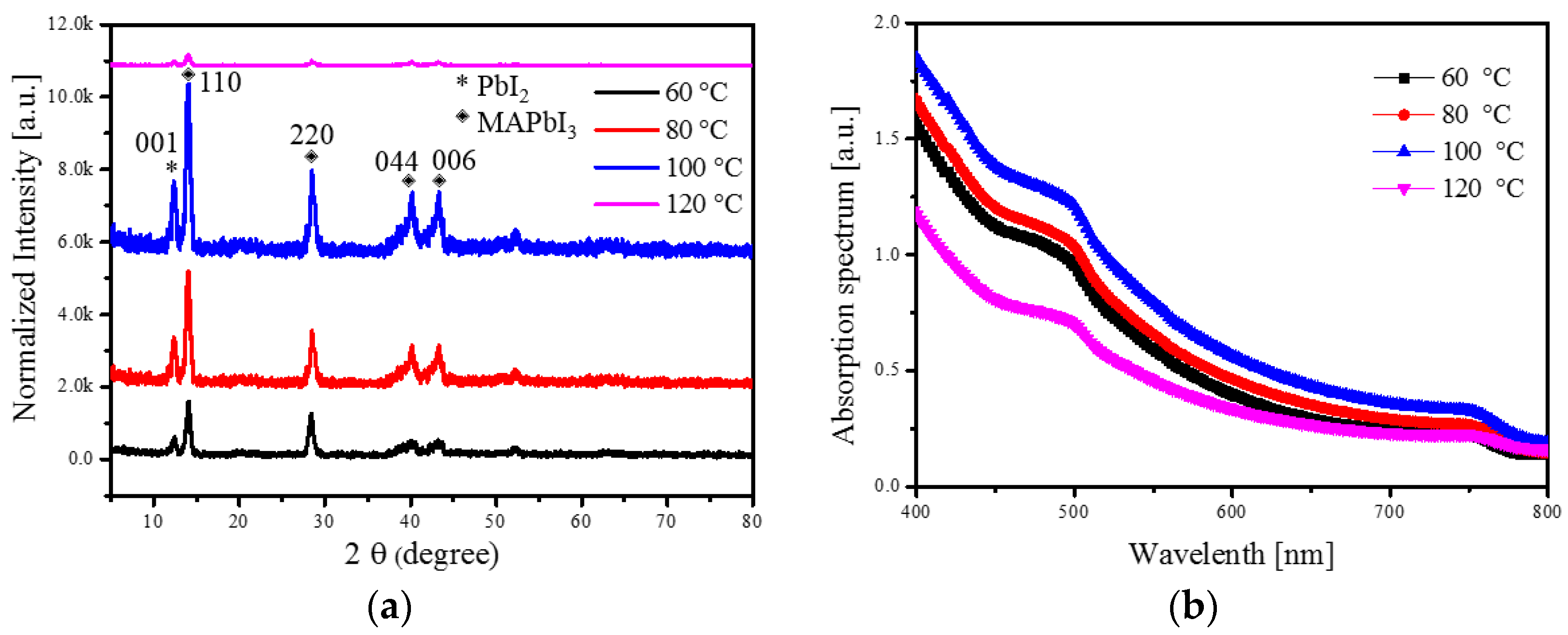
3. Results and Discussion

We used X-ray diffraction (XRD) measurements to investigate the properties of the 192 nm thick MAPbI3 layer under different annealing temperatures (60, 80, 100 and 120 °C), as shown in Figure 5a. Noticeable diffraction peaks were observed depending on the annealing temperature. The XRD patterns were composed of two phases, i.e., MAPbI3 and PbI2. For the PbI2 phase, we assigned the peak at 12.21° to the (001) plane. For the MAPbI3 phase, the peaks at 14.08, 28.46, 40.21 and 43.31° were respectively assigned to the (110), (220), (044) and (006) planes. The highest peak intensity of the perovskite layer was achieved at 100 °C. As the annealing temperature of the perovskite increased, the rate of perovskite crystallization was similarly increased, and the crystallinity improved up to the optimal temperature of 100 °C. However, when the annealing temperature exceeded the optimal temperature, i.e., up to 120 °C, the crystallinity dropped significantly, because the MAPbI3 was decomposed into PbI2, CH3NH2 and HI at an annealing temperature of 120 °C [26].
Figure 5b shows the absorption spectra of the 192 nm thick MAPbI3 layer with annealing temperatures of 60, 80, 100, and 120 °C. It was clear that the absorption intensity increased as the annealing temperature increased from 60 to 100 °C. When the annealing temperature reached 120 °C, the annealing temperature was too high, resulting in degradation in the perovskite layer. As a result, the absorption intensity decreased as the light-harvesting ability decreased. The result of the decrease of light absorption capacity was consistent with the result of XRD, which was caused by the decomposition of the MAPbI3 due to the high heating temperature.
To investigate the photovoltaic properties of the detectors based on a MAPbI3 layer under different annealing temperatures, we measured the current density-voltage (J-V) characteristics of the detector based on a 192 nm thick MAPbI3 layer, as shown in the Figure S4. The parameters including JSC, RS, CCD and sensitivity of the detectors are listed in Table 1. The device constructed with an annealing temperature of 60 °C achieved JSC of 16.39 mAcm−2, RS of 212.78 Ω, and sensitivity of 2.26 mA/Gycm2. When the active layer was annealed at 100 °C, the device yielded an improved JSC of 18.78 mAcm−2, RS of 172.23 Ω, and sensitivity of 2.84 mA/Gycm2, i.e., 25% better sensitivity compared to the use of an active layer annealed at 60 °C. In addition, to further observe the effect of different temperatures on the perovskite layer, the current density-voltage (J-V) curves of the detectors with different thicknesses of MAPbI3 active layer (109, 145 and 215 nm) were also measured (as depicted in Figures S2, S3 and S5 of Supplementary Materials). The parameters such as JSC, RS, CCD and sensitivity of the detectors are listed in Table S1–S3 (see Supplementary Materials), respectively. About 10 detectors with the MAPbI3 active layer were manufactured to verify the reproducibility.
Scanning electron microscopy (SEM) images of MAPbI3 films of different thicknesses grown on a glass/ITO/PEDOT: PSS stacked structure are shown in Figure 6a. The annealing temperature was fixed at 100 °C. The MAPbI3 film thickness depended on the spin-coating speed. From the cross-sectional SEM images, we confirmed that MAPbI3 films that were 109, 145, 192, or 215 nm thick were sequentially formed under spin rates of 3000, 3500, 4000, and 4500 rpm. To understand the effect of perovskite film thickness on the morphology, we used AFM analysis to evaluate the change in the topology of the perovskite films on the ITO-coated glass. Figure 6b shows the topographical 3D images of the perovskite thin films. The RMS surface roughness (Rq) of 109 nm, 145 nm, 192 nm, and 215 nm thick perovskite layers was 43.8 nm, 32.2 nm, 21.9 nm, and 36.8 nm, respectively. As the thickness of the perovskite film increased, the surface roughness decreased. This was because the presolution of MAPbI3 could grow more completely into a thin film. When the thickness increased to 215 nm, the surface roughness increased; this was because some of the presolution could not react completely with an excessively thick MAPbI3 layer.
Figure 7a shows the XRD characteristics of MAPbI3 films with different thicknesses at an annealing temperature of 100 °C. For all MAPbI3 peaks, the (110) phase had the highest peak intensity, while the other (220), (044) and (006) phases had relatively low peak intensities. It was confirmed that the polycrystalline MAPbI3 film had a dominant orientation in the (110) phase. As the thickness of the MAPbI3 film increased, the peak intensity of the (110) phase increased, and it was confirmed that the change in the film thickness influenced the crystallinity of the perovskite. Considering the structural stability for the (110) orientation, the 192-nm thick MAPbI3 film had higher structural stability than did the films with other thicknesses. The preferred (110) orientation of the MAPbI3 layer had superior photoelectric properties because of the improved crystalline quality.
Good absorption properties in the visible region of the active layer are important. To further understand the light absorption capacity of perovskite layers, we measured the absorption spectra of MAPbI3 layers with different thicknesses annealed at 100 °C. Figure 7b shows the absorbance curves of the perovskite layers. The absorbance of the perovskite film increased with increasing thickness. The highest absorbance was obtained with a 192 nm thick perovskite layer. When the thickness of the perovskite film exceeded 192 nm, the previous AFM and XRD measurements showed an increase in surface roughness and a decrease in crystallinity.
To investigate the photovoltaic properties of the detectors with different thicknesses of the MAPbI3 layer, we measured the current density-voltage (J-V) characteristics using the solar simulator and electrometer mentioned in Section 2.3. The J-V curves of the detectors with different thicknesses of perovskite layers are shown in Figure 8a, and parameters such as Jsc and Rs extracted from the J-V curves are listed in Table 2. The maximum JSC of 18.78 mA/cm2 and the minimum series resistance of 172.23 Ω were obtained with a film thickness of 192 nm. The optimum thickness of the active layer to improve the detector performance was selected in consideration of the following three phenomena: light-absorption [29], carrier-transport, and carrier-loss characteristics [30]. For example, a mismatch between the carrier diffusion-length and the active layer thickness can lead to a decrease in the current density (J) through carrier-loss.
Figure 8b shows the logarithmic J-V characteristics of the detectors with different thicknesses of the perovskite layers. The effect of perovskite thickness on detector performance was studied by analyzing carrier mobility. The carrier mobility was determined using the space-charge-limited-current (SCLC) method in the dark [31], and using the modified Mott-Gurney equation, as shown below:
μ = 8 9 · J · L 3 V a 2 · ε 0 · ε r
where ε0 is the permittivity of free space, εr is the relative permittivity of the perovskite layer, Va is the voltage applied across the detector, μ is the carrier mobility, and L is the thickness of the perovskite layer. The calculated mobility listed in Table 2 was 1.21 × 10⁻⁴, 1.97 × 10⁻⁴, 2.83 × 10⁻⁴, and 1.83 × 10⁻⁴ cm2/Vs for the detectors with perovskite layers with thicknesses of 109, 145, 192 and 215 nm, respectively. For example, Li. et al. successfully prepared a solar cell with a MAPbI3 active layer, and obtained SCLC mobility of 1.90 × 10⁻⁴ cm2/Vs [32]. As the thickness of the perovskite film increased, the carrier mobility increased. When the thickness of the perovskite film exceeded the optimal 192 nm thickness, the surface roughness increased and the peak of the (110) plane decreased. The mobility along the (100) direction was larger than the mobility along (001) or other directions [33], which contributed to the formation of a short migration path and increased charge extraction and collection.
We used the X-ray generator and electrometer mentioned in Section 2.3 to study the radiation properties of the detectors with different thicknesses of the MAPbI3 layer. With the scintillator-decoupled detector under artificial solar exposure, the JSC was obtained via the 0 V bias of the J-V curves. We found the JSC to be 13.56, 16.54, 18.78 and 15.32 mA/cm2 for the X-ray detectors with perovskite layers with thicknesses of 109, 145, 192, and 215 nm, respectively, as indicated in Figure 9 (left axis). We calculated the CCD and sensitivity using Equations (1) and (2) in Section 2.3. The X-ray detectors with 109, 145, 192, and 215 nm thick perovskite layers exhibited sensitivities of 2.11, 2.33, 2.84, and 2.19 mA/Gycm2, respectively (right axis in Figure 9). The highest sensitivity, i.e., 2.84 mA/Gycm2, under X-ray exposure was achieved with the detector with a 192 nm thick perovskite layer. Starkenburg et al. successfully prepared an X-ray detector based on a boron subphthalcyanine chloride (SubPc):PC60BM active layer combined with a CsI scintillator, and obtained a sensitivity of 0.96 mA/Gycm2 at a bias voltage of 1 V [34]. High sensitivity was obtained from the detector by applying the optimal conditions of annealing temperature and thickness, thereby improving the surface roughness, increasing the light absorption capacity, improving mobility, and improving the recombination loss of the perovskite layer.

4. Conclusions

In this paper, we investigated a high-sensitivity X-ray detector with a perovskite active layer for indirect X-ray detection. By changing the annealing temperature and film thickness, we could optimize the electronic and optical properties of the perovskite film applied to the active layer of the detector. First, we studied the structural properties of the MAPbI3 films prepared with different annealing temperatures (60, 80, 100, and 120 °C). The MAPbI3 film showed the highest crystallinity and absorption intensity with an annealing temperature of 100 °C. The detector with the 100 °C annealed perovskite film as the active layer had better photoelectric properties than the detector with the films annealed at other temperatures. Second, by studying the characteristics of different thicknesses (109, 145, 192 and 215 nm) of the perovskite layer, we found that the 192 nm thick layer had lowest roughness and better mobility. The detector with the perovskite layer that was 192 nm thick had better current density because of its high light-harvesting efficiency, long electron-hole diffusion length, and less carrier-recombination loss. Finally, the highest sensitivity, i.e., 2.84 mA/Gycm2, was obtained using the detector with the optimized perovskite layer. Given the many interesting properties of perovskite, such as its low-cost solution processability, highly efficient light absorption, long electron−hole diffusion length, and high carrier mobility, MAPbI3 is a promising candidate for use as an active layer applied to X-ray detectors.

Supplementary Materials

The following are available online at https://www.mdpi.com/1424-8220/20/23/6872/s1.

Author Contributions

Conceptualization, J.K.; formal analysis, H.L., J.L. and J.K.; investigation, H.L., J.L. and J.K.; data curation, H.L. and J.K.; writing—original draft preparation, H.L.and J.L.; writing—review and editing, H.L. and J.K.; visualization, H.L.; supervision, J.K.; project administration, J.K.; All authors have read and agreed to the published version of the manuscript.

Funding

This research received no external funding.

Conflicts of Interest

The authors declare no conflict of interest.

References

  1. Eames, C.; Frost, J.M.; Barnes, P.R.; O’regan, B.C.; Walsh, A.; Islam, M.S. Ionic transport in hybrid lead iodide perovskite solar cells. Nat. Commun. 2015, 6, 7497. [Google Scholar] [CrossRef] [Green Version]
  2. Roose, B.; Wang, Q.; Abate, A. The role of charge selective contacts in perovskite solar cell stability. Adv. Energy Mater. 2019, 9, 1803140. [Google Scholar] [CrossRef]
  3. Dou, L.; Yang, Y.M.; You, J.; Hong, Z.; Chang, W.H.; Li, G.; Yang, Y. Solution-processed hybrid perovskite photodetectors with high detectivity. Nat. Commun. 2014, 5, 5404. [Google Scholar] [CrossRef] [PubMed]
  4. Chen, L.C.; Lee, K.L.; Lee, K.Y.; Huang, Y.W.; Lin, R.M. Study of Metal–Semiconductor–Metal CH3NH3PbBr3 Perovskite Photodetectors Prepared by Inverse Temperature Crystallization Method. Sensors 2020, 20, 297. [Google Scholar] [CrossRef] [PubMed] [Green Version]
  5. Lin, K.; Xing, J.; Quan, L.N.; de Arquer, F.P.G.; Gong, X.; Lu, J.; Li, W. Perovskite light-emitting diodes with external quantum efficiency exceeding 20 percent. Nature 2018, 562, 245–248. [Google Scholar] [CrossRef] [PubMed]
  6. Lee, S.Y.; Kim, S.H.; Nam, Y.S.; Yu, J.C.; Lee, S.; Kim, D.B.; Jung, E.D.; Woo, J.H.; Ahn, S.; Lee, S.; et al. Flexibility of semitransparent perovskite light-emitting diodes investigated by tensile properties of the perovskite layer. Nano Lett. 2019, 19, 971–976. [Google Scholar] [CrossRef] [PubMed]
  7. Yu, W.; Li, F.; Yu, L.; Niazi, M.R.; Zou, Y.; Corzo, D.; Buttner, U. Single crystal hybrid perovskite field-effect transistors. Nat. Commun. 2018, 9, 1–10. [Google Scholar] [CrossRef] [Green Version]
  8. Chin, X.Y.; Cortecchia, D.; Yin, J.; Bruno, A.; Soci, C. Lead iodide perovskite light-emitting field-effect transistor. Nat. Commun. 2015, 6, 7383. [Google Scholar] [CrossRef]
  9. Choi, H.; Mai, C.K.; Kim, H.B.; Jeong, J.; Song, S.; Bazan, G.C.; Heeger, A.J. Conjugated polyelectrolyte hole transport layer for inverted-type perovskite solar cells. Nat. Commun. 2015, 6, 7348. [Google Scholar] [CrossRef] [Green Version]
  10. Wang, D.L.; Cui, H.J.; Hou, G.J.; Zhu, Z.G.; Yan, Q.B.; Su, G. Highly efficient light management for perovskite solar cells. Sci. Rep. 2016, 6, 18922. [Google Scholar] [CrossRef] [Green Version]
  11. Ning, W.; Wang, F.; Wu, B.; Lu, J.; Yan, Z.; Liu, X.; Hultman, L. Long Electron—Hole Diffusion Length in High-Quality Lead-Free Double Perovskite Films. Adv. Mater. 2018, 30, 1706246. [Google Scholar] [CrossRef] [PubMed]
  12. Oga, H.; Saeki, A.; Ogomi, Y.; Hayase, S.; Seki, S. Improved understanding of the electronic and energetic landscapes of perovskite solar cells: High local charge carrier mobility, reduced recombination, and extremely shallow traps. J. Am. Chem. Soc. 2014, 136, 13818–13825. [Google Scholar] [CrossRef] [PubMed]
  13. Zhang, F.; Wang, Z.; Zhu, H.; Pellet, N.; Luo, J.; Yi, C.; Liu, X.; Liu, H.; Wang, S.; Li, X.; et al. Over 20% PCE perovskite solar cells with superior stability achieved by novel and low-cost hole-transporting materials. Nano Energy 2017, 41, 469–475. [Google Scholar] [CrossRef] [Green Version]
  14. Yang, D.; Sano, T.; Yaguchi, Y.; Sun, H.; Sasabe, H.; Kido, J. Achieving 20% Efficiency for Low-Temperature-Processed Inverted Perovskite Solar Cells. Adv. Funct. Mater. 2019, 29, 1807556. [Google Scholar] [CrossRef]
  15. Tsai, H.; Liu, F.; Shrestha, S.; Fernando, K.; Tretiak, S.; Scott, B.; Vo, D.T.; Strzalka, J.; Nie, W. A sensitive and robust thin-film x-ray detector using 2D layered perovskite diodes. Sci. Adv. 2020, 6, eaay0815. [Google Scholar] [CrossRef] [Green Version]
  16. Thirimanne, H.M.; Jayawardena, K.D.G.I.; Parnell, A.J.; Bandara, R.M.I.; Karalasingam, A.; Pani, S.; Huerdler, J.E.; Lidzey, D.G.; Tedde, S.F.; Nisbet, A.; et al. High sensitivity organic inorganic hybrid X-ray detectors with direct transduction and broadband response. Nat. Commun. 2018, 9, 1–10. [Google Scholar] [CrossRef]
  17. Gill, H.S.; Elshahat, B.; Kokil, A.; Li, L.; Mosurkal, R.; Zygmanski, P.; Sajo, E.; Kumar, J. Flexible perovskite based X-ray detectors for dose monitoring in medical imaging applications. Phys. Med. 2018, 5, 20–23. [Google Scholar] [CrossRef]
  18. Wei, H.; Huang, J. Halide lead perovskites for ionizing radiation detection. Nat. Commun. 2019, 10, 1066. [Google Scholar] [CrossRef] [Green Version]
  19. Yakunin, S.; Sytnyk, M.; Kriegner, D.; Shrestha, S.; Richter, M.; Matt, G.J.; Heiss, W. Detection of X-ray photons by solution-processed lead halide perovskites. Nat. Photonics 2015, 9, 444–449. [Google Scholar] [CrossRef]
  20. Shrestha, S.; Fischer, R.; Matt, G.J.; Feldner, P.; Michel, T.; Osvet, A.; Tedde, S.F. High-performance direct conversion X-ray detectors based on sintered hybrid lead triiodide perovskite wafers. Nat. Photonics 2017, 11, 436–440. [Google Scholar] [CrossRef]
  21. Salim, T.; Sun, S.; Abe, Y.; Krishna, A.; Grimsdale, A.C.; Lam, Y.M. Perovskite-based solar cells: Impact of morphology and device architecture on device performance. J. Mater. Chem. A 2015, 3, 8943–8969. [Google Scholar] [CrossRef]
  22. Li, Y.; Ji, L.; Liu, R.; Zhang, C.; Mak, C.H.; Zou, X.; Shen, H.H.; Leu, S.Y.; Hsu, H.Y. A review on morphology engineering for highly efficient and stable hybrid perovskite solar cells. J. Mater. Chem. A 2018, 6, 12842–12875. [Google Scholar] [CrossRef]
  23. Wu, J.; Zhang, W.; Wang, Q.; Liu, S.; Du, J.; Mei, A.; Rong, Y.; Hu, Y.; Han, H. A favored crystal orientation for efficient printable mesoscopic perovskite solar cells. J. Mater. Chem. A 2020, 8, 11148–11154. [Google Scholar] [CrossRef]
  24. Muscarella, L.A.; Hutter, E.M.; Sanchez, S.; Dieleman, C.D.; Savenije, T.J.; Hagfeldt, A.; Saliba, M.; Ehrler, B. Crystal orientation and grain size: Do they determine optoelectronic properties of MAPbI3 perovskite? J. Phys. Chem. Lett. 2019, 10, 6010–6018. [Google Scholar] [CrossRef] [PubMed] [Green Version]
  25. Motta, C.; El-Mellouhi, F.; Kais, S.; Tabet, N.; Alharbi, F.; Sanvito, S. Revealing the role of organic cations in hybrid halide perovskite CH3NH3PbI3. Nat. Commun. 2015, 6, 7026. [Google Scholar] [CrossRef] [PubMed]
  26. Dualeh, A.; Tétreault, N.; Moehl, T.; Gao, P.; Nazeeruddin, M.K.; Grätzel, M. Effect of annealing temperature on film morphology of organic–inorganic hybrid pervoskite solid-state solar cells. Adv. Funct. Mater. 2014, 24, 3250–3258. [Google Scholar] [CrossRef]
  27. Tsai, H.; Asadpour, R.; Blancon, J.C.; Stoumpos, C.C.; Even, J.; Ajayan, P.M.; Kanatzidis, M.G.; Alam, M.A.; Mohite, A.D.; Nie, W. Design principles for electronic charge transport in solution-processed vertically stacked 2D perovskite quantum wells. Nat. Commun. 2018, 9, 1–9. [Google Scholar] [CrossRef]
  28. Ahn, S.; Jang, W.; Park, S.; Wang, D.H. Dry-Stamping-Transferred PC71BM Charge Transport Layer via an Interface-Controlled Polyurethane Acrylate Mold Film for Efficient Planar-Type Perovskite Solar Cells. ACS Appl. Mater. Interfaces 2017, 9, 15623–15630. [Google Scholar] [CrossRef]
  29. Wei, J.; Xu, R.P.; Li, Y.Q.; Li, C.; Chen, J.D.; Zhao, X.D.; Tang, J.X. Enhanced light harvesting in perovskite solar cells by a bioinspired nanostructured back electrode. Adv. Energy Mater. 2017, 7, 1700492. [Google Scholar] [CrossRef]
  30. Wolff, C.M.; Caprioglio, P.; Stolterfoht, M.; Neher, D. Nonradiative Recombination in Perovskite Solar Cells: The Role of Interfaces. Adv. Mater. 2019, 31, 1902762. [Google Scholar] [CrossRef] [Green Version]
  31. Moiz, S.A.; Khan, I.A.; Younis, W.A.; Karimov, K.S. Space Charge—Limited Current Model for Polymers. Conduct. Polym. 2016, 5, 91. [Google Scholar]
  32. Li, J.; Jiu, T.; Duan, C.; Wang, Y.; Zhang, H.; Jian, H.; Zhao, Y.; Wang, N.; Huang, C.; Li, Y. Improved electron transport in MAPbI3 perovskite solar cells based on dual doping graphdiyne. Nano Energy 2018, 46, 331. [Google Scholar] [CrossRef]
  33. Zhang, B.; Zhang, M.J.; Pang, S.P.; Huang, C.S.; Zhou, Z.M.; Wang, D.; Cui, G.L. Carrier transport in CH3NH3PbI3 films with different thickness for perovskite solar cells. Adv. Mater. Interfaces 2016, 3, 1600327. [Google Scholar] [CrossRef]
  34. Starkenburg, D.J.; Johns, P.M.; Baciak, J.E.; Nino, J.C.; Xue, J. Thin film organic photodetectors for indirect X-ray detection demonstrating low dose rate sensitivity at low voltage operation. J. Appl. Phys. 2017, 122, 225502. [Google Scholar] [CrossRef]
Figure 1. Energy-band diagram of the proposed detector with perovskite active layer.
Sensors 20 06872 g001
Figure 2. Solvent engineering procedure for the preparation of the perovskite precursor solution.
Sensors 20 06872 g002
Figure 3. (a) Schematics of the constructed bulk heterojunction preoskite device, (b) Fabrication procedure of the perovskite detector and solvent engineering procedure for preparing the uniform and dense perovskite film.
Sensors 20 06872 g003
Figure 4. Schematic diagram of the experimental setup for measuring the parameters of the perovskite detector without and with the CsI(Tl) scintillator.
Sensors 20 06872 g004
Figure 5. (a) XRD patterns and (b) absorption spectra of 192 nm thick MAPbI3 layer with different annealing temperatures.
Sensors 20 06872 g005
Figure 6. (a) Cross-sectional SEM images and (b) AFM images of MAPbI3 layer with different thicknesses at an annealing temperature 100 °C.
Sensors 20 06872 g006
Figure 7. (a) XRD patterns and (b) absorption spectra of MAPbI3 layer with different thicknesses at an annealing temperature 100 °C.
Sensors 20 06872 g007
Figure 8. (a) Current density-voltage (J-V) characteristics of the detectors based on a MAPbI3 layer annealed at temperature 100 °C, and (b) curve fitting of the logarithmic J-V characteristics of the detectors in the dark.
Sensors 20 06872 g008
Figure 9. JSC, CCD, and sensitivity of the detector based on MAPbI3 layer with different thicknesses at an annealing temperature 100 °C. Error bars represent the standard deviation based on 10 devices per condition.
Sensors 20 06872 g009
Table 1. JSC, RS, CCD and sensitivity of the detector based on 192 nm thick MAPbI3 layer at various annealing temperatures.
Temperature [°C]Jsc [mA/cm2]Rs [Ω]CCD [μA/cm2]Sensitivity [mA/Gy·cm2]
6016.39 ± 0.65212.78 ± 3.98.78 + 0.142.26 ± 0.07
8017.74 ± 0.62181.72 ± 3.89.41 + 0.132.43 ± 0.06
10018.78 ± 0.58172.23 ± 3.910.88 + 0.132.84 ± 0.06
12011.56 ± 0.72298.87 ± 3.87.82 + 0.131.99 ± 0.08
Table 2. JSC, RS and mobility of the detector based on MAPbI3 layer with different thicknesses at an annealing temperature 100 °C.
Layer Thickness [nm].JSC [mA/cm2]Rs [Ω]Mobility [cm2/V·s]
10913.56 ± 0.63282.11 ± 3.9(1.21 ± 0.06) × 10−4
14516.54 ± 0.61198.36 ± 3.8(1.97 ± 0.04) × 10−4
19218.78 ± 0.58172.23 ± 3.9(2.84 ± 0.04) × 10−4
21515.32 ± 0.62256.09 ± 3.8(1.83 ± 0.05) × 10−4
Publisher’s Note: MDPI stays neutral with regard to jurisdictional claims in published maps and institutional affiliations.

