Abstract
RuO2 thin films were prepared using magnetron sputtering under different deposition conditions, including direct current (DC) and radio frequency (RF) discharges, metallic/oxide cathodes, different substrate temperatures, pressures, and deposition times. The surface morphology, residual stress, composition, crystal structure, mechanical properties, and pH performances of these RuO2 thin films were investigated. The RuO2 thin films RF sputtered from a metallic cathode at 250 °C exhibited good pH sensitivity of 56.35 mV/pH. However, these films were rougher, less dense, and relatively softer. However, the DC sputtered RuO2 thin film prepared from an oxide cathode at 250 °C exhibited a pH sensitivity of 57.37 mV/pH with a smoother surface, denser microstructure and higher hardness. The thin film RF sputtered from the metallic cathode exhibited better pH response than those RF sputtered from the oxide cathode due to the higher percentage of the RuO3 phase present in this film.
1. Introduction
The sensing of pH is very important in several chemical and biological processes, such as for applications in water and food quality monitoring, and wearable systems for chronic diseases [1]. In order to optimise the desired response and to eliminate unwanted reactions, pH measurement, and control are both required in many applications, such as blood monitoring, environmental monitoring, water quality monitoring, and various clinical tests. The glass electrode sensor has been commonly used for pH measurement due to its high accuracy, fast response, and ideal Nernst behaviour. However, with the increasing requirements for different applications, glass electrodes exhibit drawbacks such as instability in high temperature environments, poor mechanical properties in high pressure environments, and difficulties in miniaturisation [1]. Therefore, many other pH measurement techniques have been developed recently, one of which is the solid-state metal oxide thin film sensor, based on oxides such as PtO2, IrO2, RuO2, SnO2, and Ta2O5, that has been demonstrated to exhibit excellent pH sensing performance at high temperatures and pressures and these are promising candidates for a future generation of pH sensors. Among these metal oxide materials, magnetron sputtered RuO2 thin films show outstanding properties with near Nernstian pH sensitivity, high conductivity, and excellent mechanical strength and corrosion resistance [2,3,4,5], as such it has been researched extensively.
Magnetron sputtering is one of the most attractive physical vapor deposition processes (PVD) for an extensive range of metal oxide materials due to its outstanding advantages, such as high deposition rate, excellent reproducibility, high density, and good quality of deposited thin films [5]. Many researchers have reported excellent pH response for radio frequency (RF) sputtered RuO2 thin films [6,7,8]. There have been many studies on the effects of different sputtering conditions on the properties and pH performance of RF sputtered RuO2 thin films, such as sputtering temperatures in the range of room temperature to 500 °C [9,10], deposition time/thin film thickness [11], and Ar/O ratios ranging between 10 and 2.3 [12,13]. However, there are few reports comparing the differences between direct current (DC) and RF sputtering of RuO2 thin films and their characteristics and pH response. Furthermore, the effects of different cathodes (either metallic or metal oxide) have not been investigated extensively.
In this study, RuO2 thin films were sputtered under different sputtering conditions, including DC/RF discharges, metallic/oxide cathodes (Ru/RuO2), different substrate temperatures (100 °C, 150 °C and 250 °C), sputtering pressures (1.0 Pa and 2.0 Pa), and thicknesses (~200 nm and ~600 nm). The structure and properties of the deposited RuO2 thin films studied include surface morphology, residual stress, crystal structure, composition, hardness, and elastic modulus. In addition, electrochemical experiments were conducted in terms of pH sensitivity and pH stability. The effect of different sputtering conditions on the RuO2 thin film properties, especially the effect of different discharges and different cathodes, were studied. Furthermore, the effect of the presence of RuO3 in these RuO2 thin films and the correlation between the pH response and—structural characteristics are discussed.
2. Materials and Methods
2.1. Thin Film Fabrication
RuO2 thin films were deposited using a magnetron sputtering system equipped with an axial turret magnetron head and power supply (AJA DCXS-750, Scituate, MA, USA). The turret head was mounted vertically in the bottom of the vacuum system. The target materials used for sputtering were metallic (Ru) cathode and oxide (RuO2) cathodes of high purity (>99.0%). The nominal size of the sputter targets was 50 mm in diameter and the distance between the cathodes and the substrate was set at 60 mm. The films were deposited onto (100) conducting silicon wafers with a resistivity of 0.05 Ω-cm. The substrates size was 25.0 mm × 25.0 mm. The substrates were electrically grounded. The deposition system was equipped with rotary and cryogenic pumps and a controlled gas introduction system. A base pressure of 1 × 10⁻⁴ Pa was attained in the chamber before the deposition. The oxygen reactive gas and argon inert gas were introduced into the chamber depending on the sputtering target used. The deposition pressure could be set independently of the gas flow by adjusting a throttle valve. The RF or DC powers were set at 100 W or 125 W, respectively. The deposition times varied between 15 to 40 min. The film thickness variation across the substrate was in order of 10.0%. Three groups of RuO2 thin films were prepared as outlined in Table 1.

Table 1.
Deposition conditions for all samples, direct current (DC) and radio frequency (RF)
- Samples S1–S3 were deposited by reactive RF sputtering from a metallic cathode target (Ru) with a fixed oxygen partial pressure (Ar/O2 ratio of 4/1), total pressure (2.0 Pa), RF power (125 W), and deposition time (20 min). The substrate temperature was varied from 100 to 250 °C.
- Samples D1–D4 were sputtered from an oxide cathode target (RuO2). D1 and D2 were deposited by DC sputtering with fixed total pressure (2.0 Pa), DC power (100 W), and deposition time (15 min). The substrate temperatures were room temperature and 250 °C respectively. D3 and D4 were deposited by rf sputtering with fixed substrate temperature (250 °C), RF power (100 W) and deposition time (20 min). The deposition pressures were 2.0 and 1.0 Pa, respectively.
- Thicker samples, T1 and T2, were deposited by DC sputtering from an oxide cathode target (RuO2) with a fixed total pressure (2.0 Pa), DC power (100 W) and longer deposition time (40 min). The substrate temperatures were 150 and 250 °C, respectively.
2.2. Film Characterisation
In order to measure the surface morphology of the thin films, a Bruker SPM ICON atomic force microscope (AFM) was employed to determine the roughness and the grain size. The residual stress in the thin films was calculated from the bending height that was measured by a Dektak 3030 surface profilometer and the thickness was determined by scanning electron microscopy (SEM) (ZEISS AURIGA) from the cross-section of the films.
X-ray photoelectron spectroscopy (XPS) measurements of all samples were performed in a SPECS SAGE 150 XPS System using Mg Kα radiation at 10 kV and 10 mA. The system operated at 100 W. The base pressure in the sample chamber of the spectrometer was <1 × 10⁻⁷ mbar. The pass energy was 30 eV with a step size of 0.5 eV for broad scanning and was 20 eV with a step size of 0.1 eV for high resolution scanning. The instrumental resolution was 1.3 eV as measured from the FWHM of the 4f7/2 line for Au at 84.0 eV. Curve fitting of the high-resolution scans and peak area calculations were carried out using Casa XPS software.
Raman scattering measurements were made using a confocal RENISHAW inVia instrument in back-scattering geometry. A solid-state laser with a wavelength of 514 nm was used as the excitation source. The laser power was 1.4 mW and the laser beam was normal to the sample surface. The laser light was focused to a spot size of about 700 nm in diameter onto the sample with an optical microscope. An exposure time of 20 s was used. The signal was detected by a charge coupled device camera and a 2400 lines/mm monochromator. The resolution of the system was about 1 cm−1.
The crystal structure of the RuO2 thin films was characterised by conventional θ−2θ X-ray diffraction using an Empyrean XRD Diffractometer with a Cu Kα (λ = 1.5406 A) source. The hardness and elastic modulus of the thin films were determined by nanoindentation tests with a Hysitron Triboindenter TI 900 using a standard Berkovich indenter. The loading force was set as 2000 μN for all samples. The pH sensitivity and stability of the RuO2 thin films was measured using the open circuit potential (OCP) method in a commercial pH buffer solution (Merck) of different pH values (pH = 2, 4, 7, 10) with a large input resistance.
3. Results and Discussion
3.1. Surface Morphology
The AFM analysis of samples in the S group and D group are shown in Figure 1 and Figure 2. The roughness values, Ra, for these samples are listed in Table 2. The roughness is assumed to increase as the grains tend to coarsen with increasing substrate temperature. From Figure 1b, the sample deposited at 150 °C shows deep voids and protruding grains which leads to a higher roughness than that for sample S3. However, based on Figure 1c, the thin film deposited at 250 °C is denser than that deposited at 150 °C, which is expected in accordance with the higher temperature. The likely reason behind this is that increasing the substrate temperature significantly enhances the lateral mobility of the condensing sputtered target atoms. Temperature-activated incoming depositing atoms tend to fill up the voids instead of self-shadowing, which in turn densifies the film material.
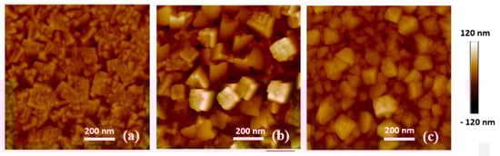
Figure 1.
Atomic force microscope (AFM) images of the S group samples; (a) S1—100 °C; (b) S2—150 °C; (c) S3—250 °C.
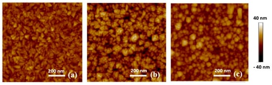
Figure 2.
AFM images of D group samples; (a) D2, (b) D3—and (c) D4.
Table 2.
Surface roughness of the RuO2 thin films.
In the sample D group, when comparing the AFM images for samples D2 and D3 (Figure 2a,b), the RF sputtered thin film has a rougher surface and larger grain size than the DC sputtered thin film. This is due to the difference in the sputtering plasma. The applied potential will vary significantly between RF and DC sputter deposition. One of the major influences on the film morphology will be the bombardment of the film by high energy (charged) species. The ions within the plasma have higher energy during RF sputtering compared to DC sputtering, which is beneficial for grain growth during deposition [14]. The grain coarsening leads to a higher surface roughness. Samples D3 and D4 in Figure 2b,c indicate that the RuO2 thin film has a smoother surface and smaller grain size when deposited at a lower sputtering pressure. Similar behaviour was also observed in the case of DC sputtered iridium oxide films deposited onto Si substrates [15]. Samples in the T group (data not shown for brevity) exhibit a relatively low roughness as they were DC sputtered.
There is a significant difference in the roughness between S group sputtered from a metallic cathode (Figure 1c) and D group sputtered from an oxide cathode (Figure 2a). This is because thin films sputtered from the metallic cathode were in an oxygen environment. The oxidation reaction occurs near the Si substrate.
3.2. XPS Analysis
All peaks in the spectra were charge corrected with respect to the C 1s peak (284.6 eV). The Ru doublet peak (Ru 3d3/2 and Ru 3d5/2) and Ru 3p peaks were identified in the wide spectral scan. Since the adventitious C 1s peak at 284.6 eV coincides with the Ru 3d3/2 peak, the use of the Ru 3d peaks for qualitative and quantitative analysis is not reliable, but there have been a few studies using the assignment of Ru 3p peaks for ruthenium oxides, especially for RuO3 peaks [16]. Thus, fitting of the Ru 3d peaks is used for identification, while the Ru 3p3/2 peak fitting is used for ratio calculations. Figure 3 shows the peak fitted spectrum for both O 1s and Ru 3d for sample S1.
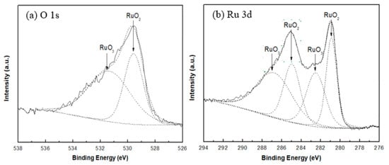
Figure 3.
(a) O 1s and (b) Ru 3d peaks region for sample S1.
From the peak fitting analysis for both the O 1s and Ru 3d peaks of sample S1 (Figure 3), two types of ruthenium oxides are identified that contribute to the structure of the deposited thin films. The peak fittings of all samples are similar, indicating that all the samples consist of two different oxide species. According to data from the published literature presented in Table 3, the reported values of RuO2 and RuO3 match the binding energies of the Ru 3d and O 1s peaks from the present XPS measurements for all samples. In this case, the ruthenium oxides present in these thin films are identified as RuO2 and RuO3.
Table 3.
XPS binding energies of different RuOx compounds from the literature.
The peak fitting for Ru 3p3/2 has approximately the same FWHM for both RuO2 and RuO3 (3.4 eV). The results of RuO2/RuO3 ratios of all samples are listed in Table 4. The results show that the RuO2 is the dominant oxide species in the thin films deposited at the lower substrate temperatures and especially in the non-oxygen sputtering environment. An obvious trend can be observed according to the samples in the S group that were reactive RF sputtered in an O2 environment, that is, the percentage of RuO3 increases as the substrate temperature increases.
Table 4.
RuO2/RuO3 ratios for all samples.
3.3. Residual Stress and Raman Spectroscopy
The results of the residual stresses in the thin films were calculated using the Stoney’s formula [20], which are listed in Table 5. The residual stress normally increases with increasing substrate temperature as the thin film becomes denser. In the S group, the compressive residual stress increases at first, but then decreases and converts to tensile stress with a further increase in temperature. The higher compressive residual stresses at higher substrate temperatures may be related to the denser microstructure that formed. However, greater grain growth at higher temperatures may also contribute to stress relaxation [21]. In addition, the tensile stress can linearly increase from the thermal mismatch between the thin film and the substrate with increasing deposition temperature [21]. In the case of sample S3, that was deposited at the highest temperature, grains coarsen, and the thermal tensile stress may exceed the intrinsic compressive stress, which resulted in a tensile residual stress in this thin film. The effect of sputtering pressure on the residual stress can also be observed from samples D3 and D4. At a lower sputtering pressure of 1.0 Pa, the compressive residual stress is higher in this thin film. The reason is that the lower sputtering pressure can give a lower sputtering rate, which is beneficial to deposit a denser thin film.
Table 5.
Residual stress for all samples.
The Raman spectra for samples in groups S and D are shown in Figure 4. Three Raman-active modes, e.g., A1g and B2g can be observed in the Raman spectra and analysis of spectra for these films can provide insight into the phase constitution of each sample. The B1g mode is too weak to be observed. For the thinner films, there is a combination of RuO2 and Si peaks at the, e.g., mode region for each sample. The possible reason is that the RuO2 thin film is deposited with a nm-scale thickness onto the Si substrate, so the incident laser penetrates the RuO2 thin film and interacts with the Si substrate. In this case, peak fitting is applied to specify the position of the, e.g., frequency mode and is also used to assign the peak position of the A1g and B2g modes for RuO2.
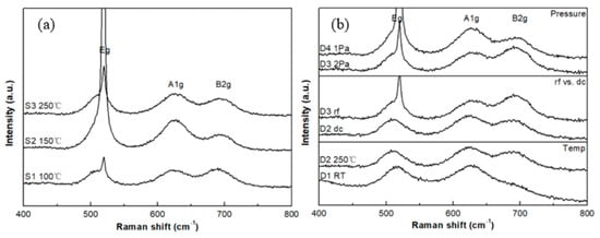
Figure 4.
Raman spectra for samples in the (a) S group (b) D group with deposition pressure, RF and DC sputtering and deposition temperature variations.
The three major Raman-active modes, e.g., A1g and B2g for single-crystal RuO2 are located at 528, 644, and 716 cm−1, respectively [22,23]. In this experiment, all the three Raman-active modes show a red shift in the peak location. The red shift has a linear relationship with the residual stress according to Meng and Dos Santos [24]. In fact, the stress should have an influence on all modes, but the stress effect on A1g mode is greater than the others [24]. Figure 5 shows the relationship between the A1g peak position and the residual stress of the S and D groups. In the case of the group D samples, films D1, D2, and D3 show that the Raman shift increases with the residual stress linearly. Sample D4 (stress = 0.82 GPa) falls out of the trend as it is the only sample deposited at a lower pressure (1.0 Pa) than the other three samples deposited at 2.0 Pa. The deposition pressure influences the bombardment energy of the depositing atoms resulting in the modifications of the properties of the films such as texture, morphology, composition and stress. The data of the group S show a non-linear relationship. This difference in the trend can be attributed to the surface morphologies and film texture between the two groups of samples. In addition, the increasing percentage of RuO3 for group S sputtered from the metallic cathode that alters the O/Ru ratio. Parker et al. [25] indicated that the Raman peak positions are dependent on the O/Ti ratio in TiO2 films.
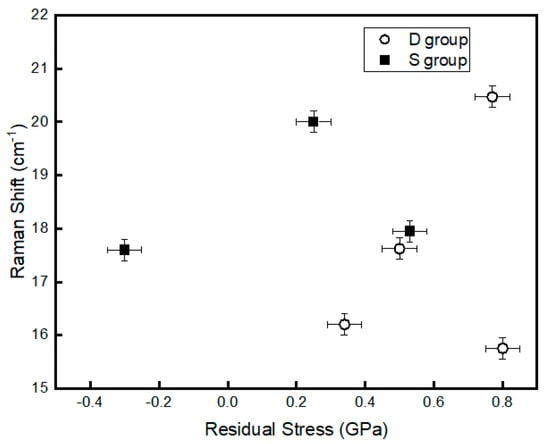
Figure 5.
The relationship between the residual stress and Raman shift for the A1g mode.
Chan et al. [26] assigned the peak at 800 cm−1 to RuO3 using surface-enhanced Raman spectroscopy. However, here the Raman results do not indicate a peak at 800 cm−1. This is likely because the region of the composition that XPS measures is only the near surface region of the thin film, while the region of the structure that Raman spectroscopy measures is much deeper into the thin film and hence the substrate (that is, a strong Si peak can be observed in the Raman spectra). The surface region may consist of RuO2 and RuO3, while the bulk region of thin film may only consist of RuO2. In this case, the RuO2 thin film can be considered as a layered structure. This is in agreement with the work of Chou et al. [8].
3.4. X-ray Diffraction Analysis
From Figure 6, for films deposited (S group) at both 100 and 150 °C, the preferred crystal orientation of RuO2 thin film is (101). With increasing substrate temperature up to 250 °C, there is a peak at (110) which increases in intensity with temperature. This result is similar to that recorded previously [27,28,29], where the RuO2 thin films show a preferred orientation along the (101) over the temperature range from 100 °C to 300 °C. There is a relatively weak (200) peak at the highest temperature of 250 °C, which was reported to increase with the temperature increases to above 300 °C [23]. All observed peaks of the RuO2 films were assigned to the tetragonal rutile structure with lattice parameters of c = 4.50 Å and c = 3.05 Å.
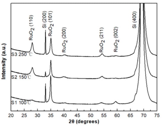
Figure 6.
X-ray diffraction patterns of samples from the S group.
For the sample prepared by RF sputtering at the lower pressure of 1.0 Pa, the thin film exhibits relatively weak crystallinity (Figure 7a). From Figure 7b, the thin film prepared by DC sputtering shows a polycrystalline structure when compared to that prepared by RF sputtering. The rf sputtered thin films exhibit the (101) preferential orientation. As the temperature increases to 250 °C, there is a change in preferential orientation from (101) to (110). For the sample prepared by DC sputtering at room temperature, (not shown here) the thin film exhibits a dominant crystal orientation of (101), which is different from the reported results where the RuO2 samples, prepared by RF sputtering, showed an amorphous structure at room temperature [27,28]. The XRD patterned of DC sputtered film deposited at 150 °C (T2) is shown in Figure 7c, exhibiting a dominant crystal orientation of (101), A broad peak was located at around 55° that indicates a short-range periodic arrangement of RuO2 (211). Compared to the samples sputtered from the metallic Ru cathode, which have polycrystalline structure (Figure 6 (S3) and Figure 7b (D3)), the thin films prepared from the RuO2 oxide cathode have a preferential (101) orientation. This is presumably because the oxidation reaction of the metal target atoms at the substrate causes the change in the deposition behaviour of the oxygen species. Compared to the sample prepared under the same condition, but with a thinner film (Figure 7b (D2) and (Figure 7c (T2)), the thicker thin film shows a strong preferential (101) orientation. In the XRD measurements, no peaks of the RuO3 phase were observed for all the samples studied here. As indicated earlier, the RuO3 phase was identified with the XPS technique which is a surface sensitive technique (~5 to 10 nm depth) where the sensitivity depth of the XRD analysis is in the micrometers range. Therefore, due to the different depth sensitivity of these techniques, one may obtain different information if the film is not homogenous with thickness. We deduce that the RuO3 is present only on the outer surface of the films and not in the bulk since no XRD peaks assigned to RuO3 were observed.
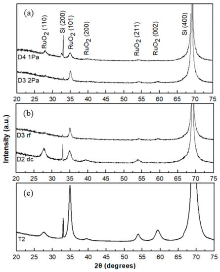
Figure 7.
X-ray diffraction patterns of the D group samples (a) RF discharge: 1.0 Pa and 2.0 Pa; (b) DC/RF difference; and (c) T2 with thicker thickness (~700 nm).
3.5. Hardness and Modulus Results
The load-unload curves for samples in the D group and T group all show good homogeneity. Figure 8 shows the load-unload curves for sample D1. The load-displacement (p-h) curves for samples in the S group, however, show a greater variation, which is mainly because of the non-ideal sample surface for these samples. The high roughness and the relatively small thickness may also contribute to this effect. In this case, the deviations of the data are large, and the results are unreliable. The hardness and elastic reduced modulus values for all samples are listed in Table 6.
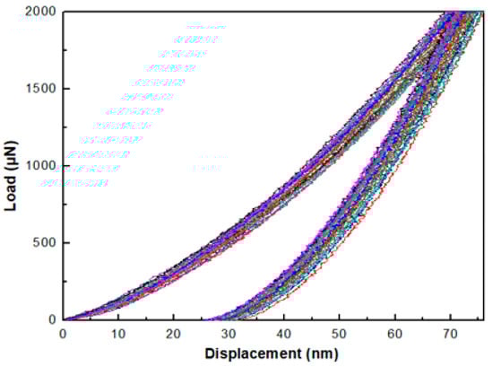
Figure 8.
Load-unload curves of sample D1 under 2000 μN maximum loading force.
Table 6.
Hardness and elastic reduced modulus for all samples.
In brief, however, the hardness increases as the substrate temperature increases because the thin films become denser at high temperature. Residual stress also influences the hardness; compressive stress makes thin films harder, while tensile stress makes thin films softer. Sample D2, that retains the highest compressive residual stress, exhibits the highest hardness. Although the hardness result for sample S3 that is under a tensile residual stress is not reliable, based on its p-h curves, it can still be observed that this thin film exhibits a relatively low hardness. The low hardness of all samples in group S may be attributed to the greater grain size and the presence of RuO3.
Sample D3, prepared by RF sputtering, is softer than sample D2 prepared by DC sputtering. This is because of the different plasma effect of RF discharges that makes the grains coarsen. Sample D4 deposited at a lower pressure exhibits a higher hardness than sample D3 due to its denser microstructure at a lower sputtering rate. The thin film hardness is highly dependent on the sputtering conditions. Búc et al. [9] reported that a sputtered RuO2 thin film exhibited a hardness of 9.4 ± 1.7 GPa, while Zhu et al. [29] reported that the thin film exhibited a hardness of 20.4 ± 2.4 GPa. The hardness results obtained in this experiment are in the range of these reported values.
3.6. Electrochemical Results
Figure 9 shows the potential of saturated calomel electrode (SCE) versus pH values for the different groups of samples. The pH sensitivity of all samples is listed in Table 7. Samples S1, S3, T1, and T2 show near-Nernstian slopes of 53.6, 56.4, 57.4, and 54.1 mV/pH, respectively.
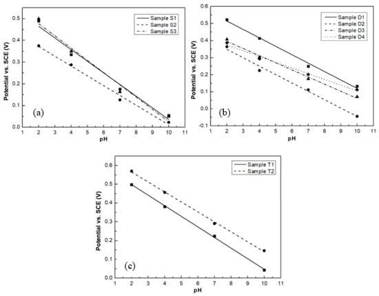
Figure 9.
pH sensitivity of samples (a) S group; (b) D group; (c) T group.
Table 7.
pH sensitivity and linearity of all samples.
The poor pH sensitivity for sample S2 could be attributed to its high porosity. From its AFM image, shown in Figure 1b, the surface exhibits deep voids and protruding grains indicating significant pore formation in the RuO2 thin film. The enhanced pore formation increases the scattering of the charge carriers and thus reduces the carrier mobility [30,31], which in turn results in the low pH sensitivity of this thin film. Furthermore, sample S2 also exhibits a potential drift. This is attributed to the trapping of hydrogen and hydroxide ions when they diffuse into the pores of the thin film [32].
When comparing the results of the pH sensitivity and the percentage of RuO3 in the thin film, from samples S1 to S3 and T1 to T2, it can be also seen that RuO2 thin films with a higher percentage of RuO3 have a better pH sensitivity. This is because a higher percentage of RuO3 leads to the higher oxygen ratio in the thin film, which increases the redox reaction speed.
In the D group, sputtered from the RuO2 cathode, it can be seen that thin films prepared by DC sputtering have a higher pH sensitivity than thin films prepared by RF sputtering. Both samples D3 and D4 exhibit the lowest pH sensitivity probably due to their smaller thickness, which is in agreement with the published literature [33], where the pH sensitivity of RuO2 electrodes decreases as their thickness decreases. This can also be seen in samples D2 and T1, which were prepared under the same sample conditions, but with different thicknesses. The pH sensitivity of the thicker sample T1 is highest. The poor pH response of the thinner RuO2 films indicates that there is insufficient RuO2 in the coating to react with the solution. This would result in the extensive exposure of the underlying Si substrate, which could form a pH dependent galvanic couple between the substrate material and solution and thus reduce the pH sensing performance.
All the samples show a stable output potential for all pH values over time, except sample S2 that exhibited a potential drift for both acidic and alkaline solutions. Figure 10 shows the potential versus time at different pH buffer solution of sample S3 as a representative example where the stability of the output is clearly evident.
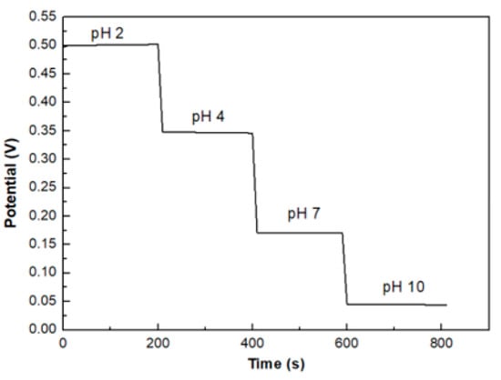
Figure 10.
pH stability of sample S3.
4. Conclusions
In this study, the effects of magnetron sputtering conditions, including DC/RF discharge, metallic/oxide cathode target, different substrate temperatures, pressures, and thicknesses, on the characterisation and pH performance of the RuO2 thin film have been investigated.
- The effects of metallic/oxide cathode. The thin films sputtered from the metallic cathode were much rougher than those sputtered from the oxide cathode due to the oxidation reaction near the substrate/as-deposited thin film and the bombardment of negative oxygen ions during sputtering process. This leads to a higher proportion of RuO3 in the thin film. The thin films sputtered from the oxide cathode were found to be much harder.
- The effects of DC/rf discharge. The RuO2 thin films deposited by RF sputtering were rougher than that deposited by DC sputtering. The rf discharge is beneficial to the grain growth in the thin film, which leads to a softer film. The DC sputtered thin films have a higher pH sensitivity response than the RF sputtered thin film.
- The effects of substrate temperature. The RuO2 thin film is rougher and denser at higher substrate temperatures due to greater grain growth. The compressive residual stress increases with increasing temperature. The percentage of RuO3 in the RuO2 thin film increases as the substrate temperature increases.
- The effects of sputtering pressure. The RuO2 thin film are rougher and less dense when deposited at a higher sputtering pressure due to the higher sputtering rate. At a lower pressure, the thin film retains a higher compressive residual stress, which results in a higher hardness. The percentage of RuO3 is higher at lower sputtering pressure.
- The effects of the presence of RuO3. The presence of RuO3 in the RuO2 thin film results in the thin film to be rougher and softer. The higher percentage of RuO3 in the thin film leads to a better pH response. The Raman red shift is related to both the residual stress and the O/Ru ratio.
- Sample S3 RF, sputtered from a metallic cathode at 250 °C, and thick sample T1, DC sputtered from the oxide cathode at 250 °C, have near-Nernstian pH sensitivities of 56.4 and 57.4 mV/pH, respectively. The RuO2 thin film RF sputtered from the metallic cathode at higher temperature exhibits a good pH performance with a thinner thickness. However, the thin film is rougher, less dense, and softer. The RuO2 thin film DC sputtered from the oxide cathode at higher temperature exhibited a good pH performance with a smoother surface, denser microstructure and higher hardness.
Author Contributions
Conceptualisation–resources, A.B.; methodology–writing—original draft preparation, X.Y.; formal analysis, M.V., F.I., and P.M. (Phil Martin); supervisions; P.M. (Paul Munroe) All authors have read and agreed to the published version of the manuscript.
Funding
This research received no external funding.
Conflicts of Interest
The authors declare no conflict of interest.
References
- Miao, Y.; Chen, J.; Keming, F. New technology for the detection of pH. J. Biochem. Biophys. Methods 2005, 63, 1–9. [Google Scholar] [CrossRef]
- Kreider, K.; Tarlov, M.; Cline, J. Sputtered Thin-Film pH electrodes of Platinum, Palladium, Ruthenium and Iridium Oxides. Sens. Actuators B Chem. 1995, 28, 167–172. [Google Scholar] [CrossRef]
- Kurzweil, P. Metal Oxides and Ion-Exchanging Surfaces as pH Sensors in Liquids: State-of-the-Art and Outlook. Sensors 2009, 2, 4955–4985. [Google Scholar] [CrossRef] [PubMed]
- Xu, B.D.; Zhang, W.D. Modification of vertically aligned carbon nanotubes with RuO2 for a solid-state pH sensor. Electrochim. Acta 2010, 55, 2859–2864. [Google Scholar] [CrossRef]
- Maurya, D.; Sardarinejad, A.; Alameh, K. Recent Developments in R.F. Magnetron Sputtered Thin Films for pH Sensing Applications—An Overview. Coatings 2014, 4, 756–771. [Google Scholar] [CrossRef]
- Maurya, D.; Sardarinejad, A.; Alameh, K. High-sensitivity pH sensor employing a sub-micron ruthenium oxide thin-film in conjunction with a thick reference electrode. Sens. Actuators A Phys. 2013, 203, 300–303. [Google Scholar] [CrossRef]
- Liao, Y.H.; Chou, J.C. Preparation and characteristics of ruthenium dioxide for pH array sensors with real-time measurement system. Sens. Actuators B Chem. 2008, 128, 603–612. [Google Scholar] [CrossRef]
- Chou, J.C.; Liu, S.I.; Chen, S.H. Sensing Characteristics of Ruthenium Films Fabricated by Radio Frequency Sputtering. Jpn. J. Appl. Phys. 2005, 44, 1403–1408. [Google Scholar] [CrossRef]
- Búc, D.; Mikula, M.; Music, D.; Helmersson, U.; Jin, P.; Nakao, S.; Li, K.Y.; Shum, P.W.; Zhou, Z.; Caplovicova, M. Ruthenium oxide films prepared by reactive unbalanced magnetron sputtering. J. Electr. Eng. 2004, 55, 39–42. [Google Scholar]
- Jia, Q.; Shi, Z.; Jiao, K.; Anderson, W.; Collins, F. Reactively sputtered RuO2 thin film resistor with near zero temperature coefficient of resistance. Thin Solid Film. 1991, 196, 29–34. [Google Scholar] [CrossRef]
- Maurya, D.; Sardarinejad, A.; Alameh, K. The effects of sensing electrode thickness on ruthenium oxide thin-film pH sensor. Sens. Actuators A Phys. 2014, 214, 15–19. [Google Scholar] [CrossRef]
- Huang, D.; Chen, J. Material characteristics and electrical property of reactively sputtered RuO2 thin films. Thin Solid Film 2001, 382, 139–145. [Google Scholar] [CrossRef]
- Maurya, D.; Sardarinejad, A.; Alameh, K.; Comini, E. The pH Sensing Properties of RF Sputtered RuO2 Thin-Film Prepared Using Different Ar/O2 Flow Ratio. Materials 2015, 8, 3352–3363. [Google Scholar] [CrossRef]
- Ellmer, K.; Wendt, R. DC and RF (reactive) magnetron sputtering of ZnO:Al films from metallic and ceramic targets: A comparative study. Surf. Coat. Technol. 1997, 21–26. [Google Scholar] [CrossRef]
- Negi, S.; Bhandari, R.; Rieth, L.; Solzbacher, F. Effect of sputtering pressure on pulsed-DC sputtered iridium oxide films. Sens. Actuators B Chem. 2009, 137, 370–378. [Google Scholar] [CrossRef]
- Morgan, D.J. Resolving ruthenium: XPS studies of common ruthenium materials. Surf. Interface Anal. 2015, 47, 1072–1079. [Google Scholar] [CrossRef]
- Linford, M.R. Introduction to Surface and Material Analysis and to Various Analytical Techniques; Vacuum Technology & Coating: Weston, CT, USA, 2014; pp. 27–32. [Google Scholar]
- Bell, W.E.; Tagami, M. High-temperature chemistry of the ruthenium—Oxygen system. J. Phys. Chem. 1963, 67, 2432–2436. [Google Scholar] [CrossRef]
- Hrbek, J.; Van Campen, D.; Malik, I. The early stages of ruthenium oxidation. J. Vac. Sci. Technol. A 1995, 13, 1409–1412. [Google Scholar] [CrossRef]
- Stoney, G.G. The tension of metallic films deposited by electrolysis. Proc. Royal. Soc. Ser. A 1909, 82, 172. [Google Scholar] [CrossRef]
- Hong, S.; Yang, K. Stress measurements of radio-frequency reactively sputtered RuO2 thin films. J. Appl. Phys. 1996, 880, 22–826. [Google Scholar] [CrossRef]
- Mar, S.; Chen, C.; Huang, Y.; Tiong, K. Characterization of RuO2 thin films by Raman spectroscopy. Appl. Surf. Sci. 1995, 90, 497–504. [Google Scholar] [CrossRef]
- Meng, L.; Teixeira, V.; Dos Santos, D. Raman spectroscopy analysis of magnetron sputtered RuO2 thin films. Thin Solid Film. 2003, 442, 93–97. [Google Scholar] [CrossRef]
- Meng, L.; Dos Santos, M. Study of residual stress on RF reactively sputtered RuO2 thin films. Thin Solid Film. 2000, 375, 29–32. [Google Scholar] [CrossRef]
- Parker, J.; Siegel, R. Raman Microprobe study of nanophase TiO2 and oxidation-induced spectral changes. J. Mater. Res. 1990, 5, 1246–1252. [Google Scholar] [CrossRef]
- Chan, H.Y.H.; Takoudis, C.G.; Weaver, M.J. High-pressure oxidation of ruthenium as probed by surface-enhanced Raman and X-ray photoelectron spectroscopies. J. Catal. 1997, 172, 336–345. [Google Scholar] [CrossRef]
- Lim, W.T.; Cho, K.R.; Lee, C.H. Structural and electrical properties of RF-sputtered RuO2 films having different conditions of preparation. Thin Solid Film. 1999, 348, 56–62. [Google Scholar] [CrossRef]
- Reddy, Y.V.; Mergel, K. Structural and electrical properties of RuO2 thin films prepared by RF-magnetron sputtering and annealing at different temperatures. J. Mater. Sci.: Mater. Electron. 2006, 17, 1029–1034. [Google Scholar] [CrossRef]
- Zhu, J.B.; Yeap, K.B.; Zeng, K.; Lu, L. Nanomechanical characterization of sputtered RuO2 thin film on silicon substrate for solid state electronic devices. Thin Solid Film. 2011, 519, 1914–1922. [Google Scholar] [CrossRef]
- Liao, Y.H.; Chou, J.C. Potentiometric Multisensor Based on Ruthenium Dioxide Thin Film with a Bluetooth Wireless and Web-Based Remote Measurement System. IEEE Sens. J. 2009, 9, 1887–1894. [Google Scholar] [CrossRef]
- Cui, H.N.; Teixeira, V.; Meng, L.J.; Martins, R.; Fortunato, E. Influence of oxygen/argon pressure ratio on the morphology, optical and electrical properties of ITO thin films deposited at room temperature. Vacuum 2008, 82, 1507–1511. [Google Scholar] [CrossRef]
- Zhuiykov, S. Morphology of Pt-doped nanofabricated RuO2 sensing electrodes and their properties in water quality monitoring sensors. Sens. Actuators B Chem. 2009, 136, 248–256. [Google Scholar] [CrossRef]
- Lonsdale, W.; Alameh, M.; Wajrak, K. Effect of conditioning protocol, redox species and material thickness on the pH sensitivity and hysteresis of sputtered RuO2 electrodes. Sensors. Actuators B Chem. 2017, 252, 251–256. [Google Scholar] [CrossRef]
Publisher’s Note: MDPI stays neutral with regard to jurisdictional claims in published maps and institutional affiliations. |
© 2020 by the authors. Licensee MDPI, Basel, Switzerland. This article is an open access article distributed under the terms and conditions of the Creative Commons Attribution (CC BY) license (http://creativecommons.org/licenses/by/4.0/).