CuO-Ga2O3 Thin Films as a Gas-Sensitive Material for Acetone Detection

 , ,
, ,  and
and 
Abstract
1. Introduction
2. Materials and Methods
2.1. Gas-Sensitive Layer Deposition
2.2. Gas-Sensing Measurements
2.3. EDS, XRD and XRR
3. Results and Discussion
3.1. Characterization
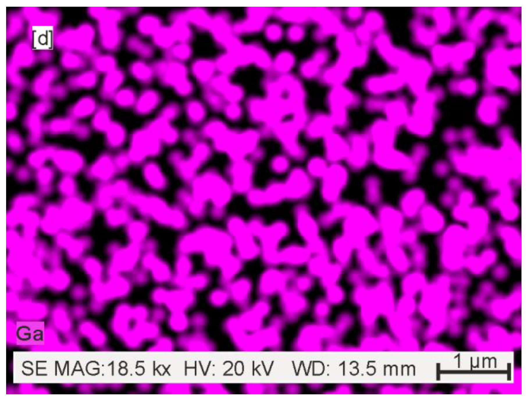
3.1.1. SEM
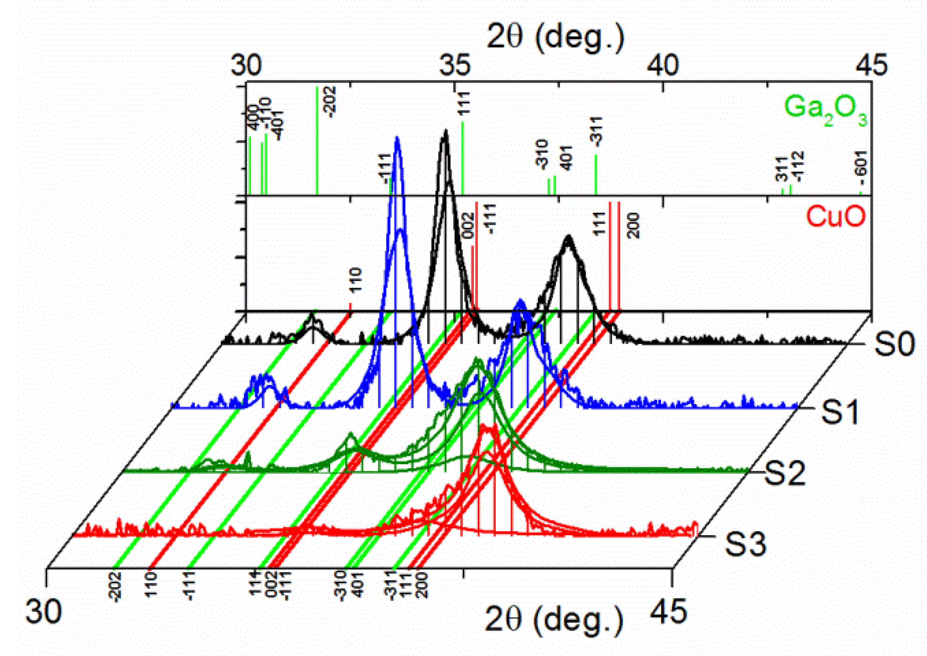
3.1.2. XRD/XRR
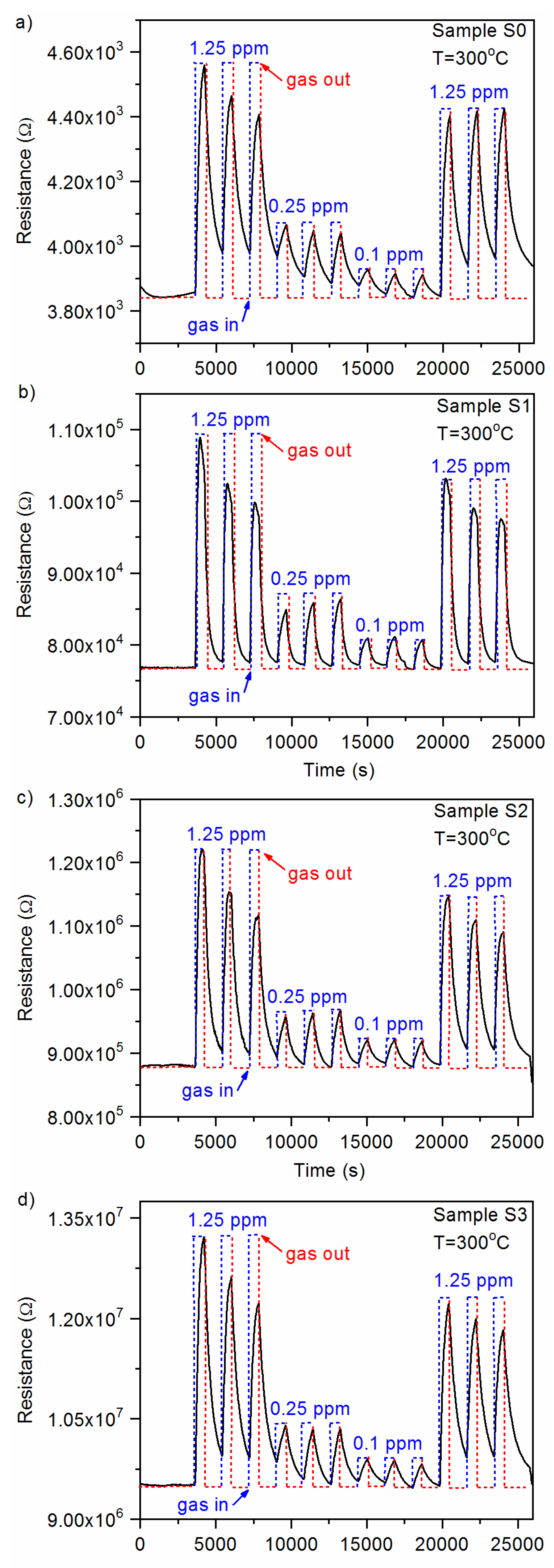
3.1.3. Gas-Sensing Characteristics
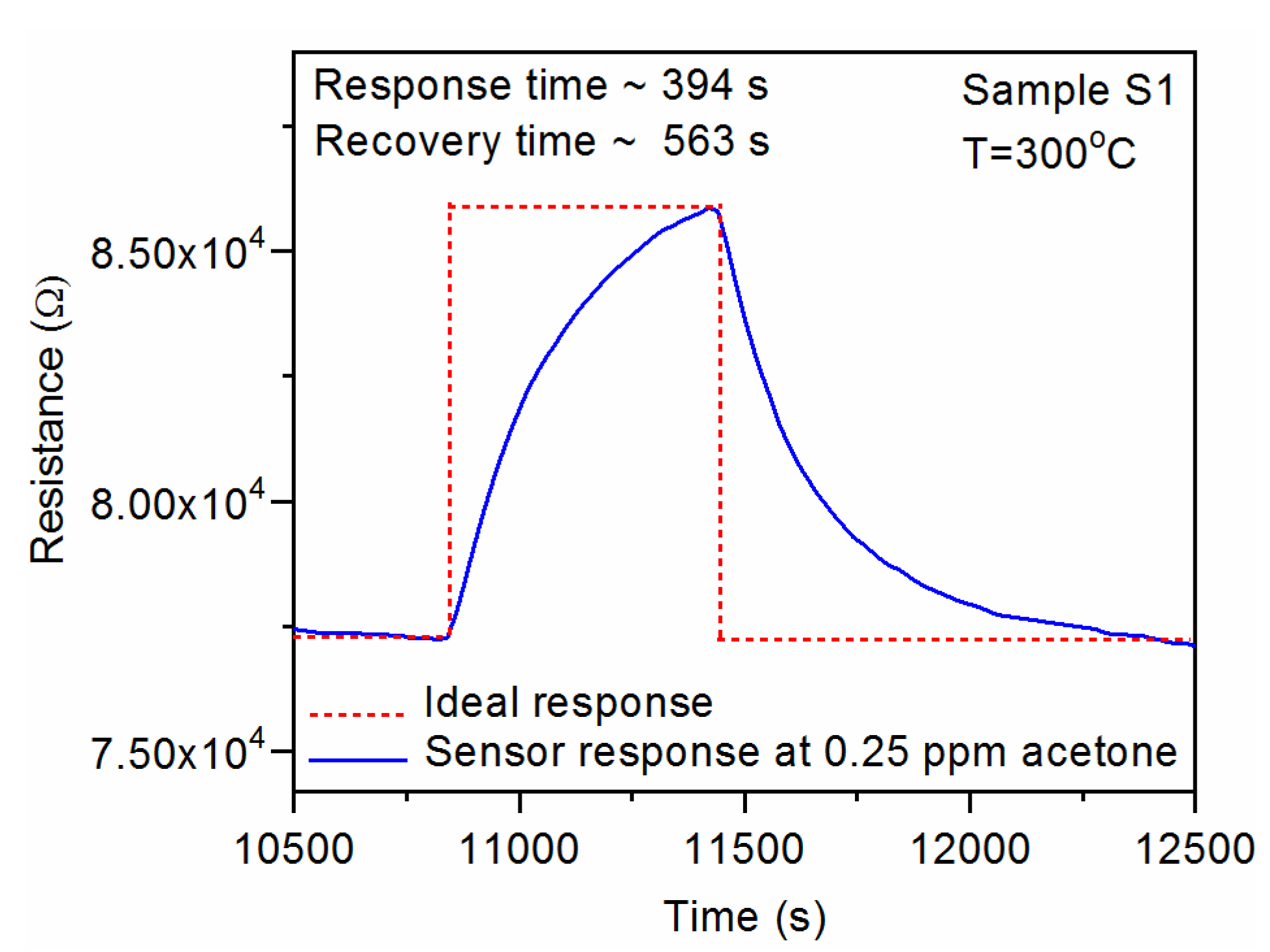
3.1.4. Response and Recovery Times
4. Conclusions
Supplementary Materials
Author Contributions
Funding
Conflicts of Interest
References
- Liu, X.; Cheng, S.; Liu, H.; Hu, S.; Zhang, D.; Ning, H. A Survey on Gas Sensing Technology. Sensors 2012, 12, 9635–9665. [Google Scholar] [CrossRef]
- Moseley, P.T. Progress in the Development of Semiconducting Metal Oxide Gas Sensors: A Review. Meas. Sci. Technol. 2017, 28, 082001. [Google Scholar] [CrossRef]
- Xu, K.; Fu, C.; Gao, Z.; Wei, F.; Ying, Y.; Xu, C.; Fu, G. Nanomaterial-Based Gas Sensors: A Review. Instrum. Sci. Technol. 2018, 46, 115–145. [Google Scholar] [CrossRef]
- Nazemi, H.; Joseph, A.; Park, J.; Emadi, A. Advanced Micro-and Nano-Gas Sensor Technology: A Review. Sensors 2019, 19, 1285. [Google Scholar] [CrossRef]
- Feng, S.; Farha, F.; Li, Q.; Wan, Y.; Xu, Y.; Zhang, T.; Ning, H. Review on Smart Gas Sensing Technology. Sensors 2019, 19, 3760. [Google Scholar] [CrossRef]
- Guan, W.; Tang, N.; He, K.; Hu, X.; Li, M.; Li, K. Gas-Sensing Performances of Metal Oxide Nanostructures for Detecting Dissolved Gases: A Mini Review. Front. Chem. 2020, 8, 76. [Google Scholar] [CrossRef]
- Iqbal, K.; Ikram, M.; Afzal, M.; Ali, S. Efficient, Low-Dimensional Nanocomposite Bilayer CuO/ZnO Solar Cell at Various Annealing Temperatures. Mater. Renew. Sustain. Energy 2018, 7, 4. [Google Scholar] [CrossRef]
- Song, H.J.; Seo, M.H.; Choi, K.W.; Jo, M.S.; Yoo, J.Y.; Yoon, J.B. High-Performance Copper Oxide Visible-Light Photodetector via Grain-Structure Model. Sci. Rep. 2019, 9, 1–10. [Google Scholar] [CrossRef]
- Di Benedetto, A.; Landi, G.; Lisi, L. Improved CO-PROX Performance of CuO/CeO2 Catalysts by Using Nanometric Ceria as Support Almerinda. Catal. Artic. 2018, 8, 209. [Google Scholar]
- Poreddy, R.; Engelbrekt, C.; Riisager, A. Copper Oxide as Efficient Catalyst for Oxidative Dehydrogenation of Alcohols with Air. Catal. Sci. Technol. 2015, 5, 2467–2477. [Google Scholar] [CrossRef]
- Electrode, N.; Sridara, T.; Upan, J.; Saianand, G.; Tuantranont, A. Non-Enzymatic Amperometric Glucose Sensor Based on Carbon Nanodots and Copper Oxide. Sensors 2020, 20, 808. [Google Scholar]
- Sayson, L.V.A.; Lopez, J.M.; Estacio, E.S.; Salvador, A.A.; Somintac, A.S. Nanostructured CuO Thin Film Deposited on Stainless Steel Using Spray Pyrolysis as Supercapacitor Electrode Nanostructured CuO Thin Film Deposited on Stainless Steel Using Spray Pyrolysis as Supercapacitor Electrode. Mater. Res. Express 2019, 6, 125551. [Google Scholar] [CrossRef]
- Deng, Z.; Ma, Z.; Li, Y.; Li, Y.; Chen, L.; Yang, X.; Wang, H. Boosting Lithium-Ion Storage Capability in CuO Nanosheets via Synergistic Engineering of Defects and Pores. Front. Chem. 2018, 6, 428. [Google Scholar] [CrossRef]
- Sundar, S.; Venkatachalam, G. Biosynthesis of Copper Oxide (CuO) Nanowires and Their Use for the Electrochemical Sensing of Dopamine. Nanomaterials 2018, 8, 823. [Google Scholar] [CrossRef] [PubMed]
- Rydosz, A.; Dyndał, K.; Andrysiewicz, W.; Grochala, D.; Marszałek, K. GLAD Magnetron Sputtered Ultra-Thin Copper Oxide Films for Gas-Sensing Application. Coatings 2020, 10, 378. [Google Scholar] [CrossRef]
- Rydosz, A. The Use of Copper Oxide Thin Films in Gas-Sensing Applications. Coatings 2018, 8, 425. [Google Scholar] [CrossRef]
- Rydosz, A.; Szkudlarek, A. Gas-Sensing Performance of M-Doped CuO-Based Thin Films Working at Different Temperatures upon Exposure to Propane. Sensors 2015, 15, 20069–20085. [Google Scholar] [CrossRef]
- Molavi, R.; Sheikhi, M.H. Materials Science in Semiconductor Processing Facile Wet Chemical Synthesis of Al Doped CuO Nanoleaves for Carbon Monoxide Gas Sensor Applications. Mater. Sci. Semicond. Process. 2020, 106, 104767. [Google Scholar] [CrossRef]
- Choi, Y.; Kim, D.; Hong, S. Sensors and Actuators B: Chemical p-Type Aliovalent Li(I) or Fe(III)-Doped CuO Hollow Spheres Self-Organized by Cationic Complex Ink Printing: Structural and Gas Sensing Characteristics. Sens. Actuators B Chem. 2018, 243, 262–270. [Google Scholar] [CrossRef]
- Wang, R.; Lin, S.; Liu, J. Li/Na-Doped CuO Nanowires and Nanobelts: Enhanced Electrical Properties and Gas Detection at Room Temperature. J. Alloys Compd. 2017, 696, 79–85. [Google Scholar] [CrossRef]
- Alarrouqi, R.A.; Saleh, B.; Haik, Y.; Al-sulaiti, L.A. Selective Gas Sensors Using Graphene and CuO Nanorods. Sens. Actuators A Phys. 2018, 283, 107–112. [Google Scholar]
- Hu, X.; Zhu, Z.; Chen, C.; Wen, T.; Zhao, X.; Xie, L. Highly Sensitive H2S Gas Sensors Based on Pd-Doped CuO Nanoflowers with Low Operating Temperature. Sens. Actuators B Chem. 2017, 253, 809–817. [Google Scholar] [CrossRef]
- Lupan, O.; Postica, V.; Ababii, N.; Hoppe, M.; Cretu, V.; Tiginyanu, I.; Sontea, V.; Pauporté, T.; Viana, B.; Adelung, R. Influence of CuO Nanostructures Morphology on Hydrogen Gas Sensing Performances. Microelectron. Eng. 2016, 164, 63–70. [Google Scholar] [CrossRef]
- Etape, E.P.; Ngolui, L.J.; Foba-tendo, J.; Yufanyi, D.M.; Namondo, B.V. Synthesis and Characterization of CuO, TiO2, and CuO-TiO2 Mixed Oxide by a Modified Oxalate Route. J. Appl. Chem. 2017, 2017, 1–10. [Google Scholar] [CrossRef]
- Ahamad, T.; Naushad, M.; Alshheri, S.M. Fabrication of Highly Porous N/S Doped Carbon Embedded with CuO/CuS Nanoparticles for NH3 Gas Sensing. Mater. Lett. 2020, 268, 127515. [Google Scholar] [CrossRef]
- Na, H.; Zhang, X.; Zhang, M.; Deng, Z.; Cheng, X.; Huo, L. Sensors and Actuators B: Chemical A Fast Response/ Recovery Ppb-Level H2S Gas Sensor Based on Porous CuO/ZnO Heterostructural Tubule via Con Fi Ned e Ff Ect of Absorbent Cotton. Sens. Actuators B Chem. 2019, 297, 126816. [Google Scholar] [CrossRef]
- Wang, X.; Li, S.; Xie, L.; Li, X.; Lin, D.; Zhu, Z. Low-Temperature and Highly Sensitivity H2S Gas Sensor Based on ZnO/CuO Composite Derived from Bimetal Metal-Organic Frameworks. Ceram. Int. 2020. [Google Scholar] [CrossRef]
- Navale, Y.H.; Navale, S.T.; Stadler, F.J.; Ramgir, N.S.; Patil, V.B. Enhanced NO2 Sensing Aptness of ZnO Nanowire/CuO Nanoparticle Heterostructure-Based Gas Sensors. Ceram. Int. 2018, 45, 1513–1522. [Google Scholar] [CrossRef]
- Li, S.; Xie, L.; He, M.; Hu, X.; Luo, G.; Chen, C.; Zhu, Z. Metal-Organic Frameworks-Derived Bamboo-Like CuO/In2O3 Heterostructure for High-Performance H2S Gas Sensor with Low Operating Temperature. Sens. Actuators B Chem. 2020, 310, 127828. [Google Scholar] [CrossRef]
- Zhou, Y.; Wang, J.; Li, X. Flexible Room-Temperature Gas Sensor Based on Poly (Para-Phenylene Terephthalamide) Fibers Substrate Coupled with Composite NiO@CuO Sensing Materials for Ammonia Detection. Ceram. Int. 2020, 46, 13827–13834. [Google Scholar] [CrossRef]
- Sui, L.; Yu, T.; Zhao, D.; Cheng, X.; Zhang, X.; Wang, P.; Xu, Y.; Gao, S.; Zhao, H.; Gao, Y.; et al. In Situ Deposited Hierarchical CuO/NiO Nanowall Arrays Film Sensor with Enhanced Gas Sensing Performance to H2S. J. Hazard. Mater. 2019, 385, 121570. [Google Scholar] [CrossRef] [PubMed]
- He, M.; Xie, L.; Zhao, X.; Hu, X.; Li, S.; Zhu, Z. Highly Sensitive and Selective H2S Gas Sensors Based on Fl Ower-like WO3/CuO Composites Operating at Low/Room Temperature. J. Alloys Compd. 2019, 788, 36–43. [Google Scholar] [CrossRef]
- Sakthivel, B.; Nammalvar, G. Selective Ammonia Sensor Based on Copper Oxide/Reduced Graphene Oxide Nanocomposite. J. Alloys Compd. 2019, 788, 422–428. [Google Scholar] [CrossRef]
- Li, Z.; Liu, Y.; Guo, D.; Guo, J.; Su, Y. Room-Temperature Synthesis of CuO/Reduced Graphene Oxide Nanohybrids for High-Performance NO2 Gas Sensor. Sens. Actuators B Chem. 2018, 271, 306–310. [Google Scholar] [CrossRef]
- Yang, B.; Liu, J.; Qin, H.; Liu, Q.; Jing, X.; Zhang, H.; Li, R. PtO2 -Nanoparticles Functionalized CuO Polyhedrons for n-Butanol Gas Sensor Application. Ceram. Int. 2018, 44, 10426–10432. [Google Scholar] [CrossRef]
- Park, S.; Cai, Z.; Lee, J.; Yoon, J., II; Chang, S. Fabrication of a Low-Concentration H2S Gas Sensor Using CuO Nanorods Decorated with Fe2O3 Nanoparticles. Mater. Lett. 2016, 181, 231–235. [Google Scholar] [CrossRef]
- Tan, W.; Yu, Q.; Ruan, X.; Huang, X. Design of SnO2-Based Highly Sensitive Ethanol Gas Sensor Based on Quasi Molecular-Cluster Imprinting Mechanism. Sens. Actuators B Chem. 2015, 212, 47–54. [Google Scholar] [CrossRef]
- Ayesh, A.I.; Alyafei, A.A.; Anjum, R.S.; Mohamed, R.M.; Abuharb, M.B.; Salah, B.; El-muraikhi, M. Production of Sensitive Gas Sensors Using CuO/SnO2 Nanoparticles. Appl. Phys. A 2019, 125, 550. [Google Scholar] [CrossRef]
- Shang, Y.; Shi, W.; Zhao, R.; Ahmed, M.; Li, J.; Du, J. Simple Self-Assembly of 3D Laminated CuO/SnO2 Hybrid for the Detection of Triethylamine. Chin. Chem. Lett. 2020. [Google Scholar] [CrossRef]
- Chen, T.; Chinnapaiyan, S.; Chen, S.; Ali, M.A.; Elshikh, M.S.; Mahmoud, A.H. Feasible Sonochemical Approach to Synthesize CuO@CeO2 Nanomaterial and Their Enhanced Non-Enzymatic Sensor Performance towards Neurotransmitter. Ultrason. Sonochem. 2019, 63, 104903. [Google Scholar] [CrossRef]
- Choi, S.; Park, J.Y.; Kim, S.S. Growth Behavior and Sensing Properties of Nanograins in CuO Nanofibers. Chem. Eng. J. 2011, 172, 550–556. [Google Scholar] [CrossRef]
- Hou, L.; Zhang, C.; Li, L.; Du, C.; Li, X.; Kang, X.-F.; Chen, W. CO Gas Sensors Based on P-Type CuO Nanotubes and CuO Nanocubes: Morphology and Surface Structure Effects on the Sensing Performance. Talanta 2018, 188, 41–49. [Google Scholar] [CrossRef] [PubMed]
- Shankar, P.; Bosco, J.; Rayappan, B. Gas Sensing Mechanism of Metal Oxides: The Role of Ambient Atmosphere, Type of Semiconductor and Gases-A Review. Sci. Lett. J. 2015, 4, 126. [Google Scholar]
- Aslani, A.; Oroojpour, V. CO Gas Sensing of CuO Nanostructures, Synthesized by an Assisted Solvothermal Wet Chemical Route. Phys. B Phys. Condens. Matter 2011, 406, 144–149. [Google Scholar] [CrossRef]
- Kim, J.; Katoch, A.; Choi, S.; Kim, S.S. Growth and Sensing Properties of Networked P-CuO Nanowires. Sens. Actuators B Chem. 2014, 212, 190–195. [Google Scholar] [CrossRef]
- Nakate, U.T.; Hee, G.; Ahmad, R.; Patil, P.; Hahn, Y.; Yu, Y.T.; Suh, E. Nano-Bitter Gourd like Structured CuO for Enhanced Hydrogen Gas Sensor Application. Int. J. Hydrogen Energy 2018, 43, 22705–22714. [Google Scholar] [CrossRef]
- Rodriguez, A.; Kim, J.Y.; Hanson, J.C.; Pe, M. Reduction of CuO in H2: In Situ Time-Resolved XRD Studies. Catal. Lett. 2003, 85, 247–254. [Google Scholar] [CrossRef]
- Hermawan, A.; Asakura, Y.; Inada, M.; Yin, S. A Facile Method for Preparation of Uniformly Decorated-Spherical SnO2 by CuO Nanoparticles for Highly Responsive Toluene Detection at High Temperature. J. Mater. Sci. Technol. 2020, 51, 119–129. [Google Scholar] [CrossRef]
- Online, V.A.; Li, H.; Sun, Y.; Chang, F.; Deng, H.; Xie, L.; Li, H. High Sensitive Gas Sensor Based on CuO Nanoparticles Synthetized by Sol-Gel Method. R. Soc. Chem. 2016, 6, 79343–79349. [Google Scholar]
- Varma, G.D. Enhanced Room Temperature Sensitivity of Ag-CuO Nanobrick/Reduced Graphene Oxide Composite for NO2. J. Alloys Compd. 2019, 806, 1469–1480. [Google Scholar]
- Hozak, P.; Vorokhta, M.; Khalakhan, I.; Jarkovska, K.; Cibulkova, J.; Fitl, P.; Vlcek, J.; Fara, J.; Tomecek, D.; Vorokhta, M.; et al. New Insight into the Gas Sensing Properties of CuOx Nanowires by Near Ambient Pressure XPS New Insight into the Gas Sensing Properties of CuOx Nanowires by Near Ambient Pressure XPS. J. Phys. Chem. C 2019, 123, 29739–29749. [Google Scholar] [CrossRef]
- Hu, J.; Zou, C.; Su, Y.; Li, M.; Han, Y.; Kong, E.S.W.; Yang, Z.; Zhang, Y. Ultrasensitive NO2 Gas Sensor Based on Hierarchical Cu2O/CuO Mesocrystals Nanoflower. J. Mater. Chem. A 2018, 6, 17120–17131. [Google Scholar] [CrossRef]
- Maximilian, F.; Meixner, H. Gallium Oxide Thin Films: A New Material for High-Temperature Oxygen Sensors. Sens. Actuators B 2000, 4, 437–441. [Google Scholar]
- Roy, R.; Hill, V.G.; Osborn, E.F. Polymorphism of Ga2O3 and the System Ga2O3-H2O. J. Am. Chem. Soc. 1952, 74, 719–722. [Google Scholar] [CrossRef]
- Togashi, R.; Nomura, K.; Eguchi, C.; Fukizawa, T.; Goto, K.; Thieu, Q.T.; Murakami, H.; Kumagai, Y.; Kuramata, A.; Yamakoshi, S.; et al. Thermal Stability of β-Ga2O3 in Mixed Flows of H2 and N2. Jpn. J. Appl. Phys. 2015, 54, 041102. [Google Scholar] [CrossRef]
- Mazeina, L.; Bermudez, V.M.; Perkins, F.K.; Arnold, S.P.; Prokes, S.M. Interaction of Functionalized Ga2O3 NW-Based Room Temperature Gas Sensors with Different Hydrocarbons. Sens. Actuators B Chem. 2010, 151, 114–120. [Google Scholar] [CrossRef]
- Chang, P.; Fan, Z.; Tseng, W.; Rajagopal, A.; Lu, J.G.; Chang, P.; Fan, Z.; Tseng, W.; Rajagopal, A.; Lu, J.G. β-Ga2O3 Nanowires: Synthesis, Characterizatio, and p-Channel Field-Effect Transistor. Appl. Phys. Lett. 2009, 222102, 88–91. [Google Scholar] [CrossRef][Green Version]
- Zheng, S.U.N.; Linhong, Y.; Xuechu, S.; Zhanghai, C. Anisotropic Raman Spectroscopy of a Single Ga2O3 Nanobelt. Chin. Sci. Bull. 2012, 57, 565–568. [Google Scholar]
- Zhang, Z.; Wang, X. Phase Transition of Two-Dimensional β-Ga2O3 Nanosheets from Ultrathin γ-Ga2O3 Nanosheets and Their Photocatalytic Hydrogen Evolution Activities. ACS Omega 2018, 3, 14469–14476. [Google Scholar] [CrossRef]
- Guo, D.; Guo, Q.; Chen, Z.; Wu, Z.; Li, P.; Tang, W. Review of Ga2O3-Based Optoelectronic Devices. Mater. Today Phys. 2019, 11, 100157. [Google Scholar] [CrossRef]
- Nakagomi, S.; Sai, T.; Kokubun, Y. Hydrogen Gas Sensor with Self Temperature Compensation Based on β-Ga2O3 Thin Film. Sens. Actuators B Chem. 2013, 187, 413–419. [Google Scholar] [CrossRef]
- Orita, M.; Hiramatsu, H.; Ohta, H.; Hirano, M.; Hosono, H. Preparation of Highly Conductive, Deep Ultraviolet Transparent Ga2O3 Thin Film at Low Deposition Temperatures. Thin Solid Films 2002, 411, 134–139. [Google Scholar] [CrossRef]
- Cuong, N.D.; Park, Y.W.; Yoon, S.G. Microstructural and Electrical Properties of Ga2O3 Nanowires Grown at Various Temperatures by Vapor-Liquid-Solid Technique. Sens. Actuators B Chem. 2009, 140, 240–244. [Google Scholar] [CrossRef]
- Frank, J.; Fleischer, M.; Meixner, H. Gas-Sensitive Electrical Properties of Pure and Doped Semiconducting Ga2O3 Thick Films. Sens. Actuators B Chem. 1998, 48, 318–321. [Google Scholar] [CrossRef]
- Shan, F.K.; Liu, G.X.; Lee, W.J.; Lee, G.H.; Kim, I.S.; Shan, F.K.; Liu, G.X.; Lee, W.J.; Lee, G.H.; Kim, I.S.; et al. Structural, Electrical, and Optical Properties of Transparent Gallium Oxide Thin Films Grown by Plasma-Enhanced Atomic Layer Deposition. J. Appl. Phys. 2005, 98, 023504. [Google Scholar] [CrossRef]
- Shi, Q.; Wang, Q.; Zhang, D.; Wang, Q.; Li, S.; Wang, W.; Fan, Q.; Zhang, J. Structural, Optical and Photoluminescence Properties of Ga2O3 Thin Films Deposited by Vacuum Thermal Evaporation. J. Lumin. 2019, 206, 53–58. [Google Scholar] [CrossRef]
- Hoefer, U.; Frank, J.; Fleischer, M. High Temperature Ga2O3-Gas Sensors and SnO2-Gas Sensors: A Comparison. Sens. Actuators B Chem. 2001, 78, 6–11. [Google Scholar] [CrossRef]
- Wang, J.; Ye, L.; Wang, X.; Zhang, H.; Li, L.; Kong, C.; Li, W. High Transmittance β-Ga2O3 Thin Films Deposited by Magnetron Sputtering and Post-Annealing for Solar-Blind Ultraviolet Photodetector. J. Alloys Compd. 2019, 803, 9–15. [Google Scholar] [CrossRef]
- Yusa, S.; Oka, D.; Fukumura, T. High κ dielectric ϵ-Ga2O3 Stabilized in a Transparent Heteroepitaxial Structure Grown by Mist CVD at Atmospheric Pressure. CrystEngComm 2019, 22, 381–385. [Google Scholar] [CrossRef]
- Higashiwaki, M.; Sasaki, K.; Kuramata, A.; Masui, T.; Yamakoshi, S. Development of Gallium Oxide Power Devices. Phys. Status Solidi Appl. Mater. Sci. 2014, 211, 21–26. [Google Scholar] [CrossRef]
- Frank, J.; Fleischer, M.; Meixner, H.; Feltz, A. Enhancement of Sensitivity and Conductivity of Semiconducting Ga2O3 Gas Sensors by Doping with SnO2. Sens. Actuators B Chem. 1998, 49, 110–114. [Google Scholar] [CrossRef]
- Li, Y.; Trinchi, A.; Wlodarski, W.; Galatsis, K.; Kalantar-Zadeh, K. Investigation of the Oxygen Gas Sensing Performance of Ga2O3 Thin Films with Different Dopants. Sens. Actuators B Chem. 2003, 93, 431–434. [Google Scholar] [CrossRef]
- Afzal, A. β-Ga2O3 Nanowires and Thin Films for Metal Oxide Semiconductor Gas Sensors: Sensing Mechanisms and Performance Enhancement Strategies. J. Mater. 2019, 5, 542–557. [Google Scholar] [CrossRef]
- Nagarajan, V.; Chandiramouli, R. Methane Adsorption Characteristics on β-Ga2O3 Nanostructures: DFT Investigation. Appl. Surf. Sci. 2015, 344, 65–78. [Google Scholar] [CrossRef]
- Wu, N.; Chen, Z.; Xu, J.; Chyu, M.; Mao, S.X. Impedance-Metric Pt/YSZ/Au-Ga2O3 Sensor for CO Detection at High Temperature. Sens. Actuators B Chem. 2005, 110, 49–53. [Google Scholar] [CrossRef]
- Mohammadi, M.R.; Fray, D.J. Semiconductor TiO2-Ga2O3 Thin Film Gas Sensors Derived from Particulate Sol-Gel Route. Acta Mater. 2007, 55, 4455–4466. [Google Scholar] [CrossRef]
- Weh, T.; Frank, J.; Fleischer, M.; Meixner, H. On the Mechanism of Hydrogen Sensing with SiO2 Modificated High Temperature Ga2O3 Sensors. Sens. Actuators B Chem. 2001, 78, 202–207. [Google Scholar] [CrossRef]
- Jang, Y.G.; Kim, W.S.; Kim, D.H.; Hong, S.H. Fabrication of Ga2O3/SnO2 Core-Shell Nanowires and Their Ethanol Gas Sensing Properties. J. Mater. Res. 2011, 26, 2322–2327. [Google Scholar] [CrossRef]
- Park, S.; Kim, S.; Sun, G.; Lee, C. Synthesis, Structure and Ethanol Sensing Properties of Ga2O3-Core/WO3-Shell Nanostructures. Thin Solid Films 2015, 591, 341–345. [Google Scholar] [CrossRef]
- Janowitz, C.; Scherer, V.; Mohamed, M.; Krapf, A.; Dwelk, H.; Manzke, R.; Galazka, Z.; Uecker, R.; Irmscher, K.; Fornari, R. Experimental electronic structure of In2O3 and Ga2O3. New J. Phys. 2011, 13, 085014. [Google Scholar] [CrossRef]
- Jin, C.; Park, S.; Kim, H.; Lee, C. Ultrasensitive Multiple Networked Ga2O3-Core/ZnO-Shell Nanorod Gas Sensors. Sens. Actuators B Chem. 2012, 161, 223–228. [Google Scholar] [CrossRef]
- Frank, J.; Fleischer, M.; Meixner, H. Electrical Doping of Gassensitive, Semiconducting Ga2O3 Thin Films. Sens. Actuators B Chem. 1996, 34, 373–377. [Google Scholar] [CrossRef]
- Pohle, R.; Fleischer, M.; Meixner, H. In Situ Infrared Emission Spectroscopic Study of the Adsorption of H2O and Hydrogen-Containing Gases on Ga2O3 Gas Sensors. Sens. Actuators B Chem. 2000, 68, 151–156. [Google Scholar] [CrossRef]
- Manandhar, S.; Battu, A.K.; Devaraj, A.; Shutthanandan, V.; Thevuthasan, S.; Ramana, C.V. Rapid Response High Temperature Oxygen Sensor Based on Titanium Doped Gallium Oxide. Sci. Rep. 2020, 10, 1–9. [Google Scholar] [CrossRef]
- Schwebel, T.; Fleischer, M.; Meixner, H.; Kohl, C.D. CO-Sensor for Domestic Use Based on High Temperature Stable Ga2O3 Thin Films. Sens. Actuators B Chem. 1998, 49, 46–51. [Google Scholar] [CrossRef]
- Pilliadugula, R.; Krishnan, N.G. Effect of PH Dependent Morphology on Room Temperature NH3 Sensing Performances of β-Ga2O3. Mater. Sci. Semicond. Process. 2020, 112, 105007. [Google Scholar] [CrossRef]
- Pandeeswari, R.; Jeyaprakash, B.G. High Sensing Response of β-Ga2O3 Thin Film towards Ammonia Vapours: Influencing Factors at Room Temperature. Sens. Actuators B Chem. 2014, 195, 206–214. [Google Scholar] [CrossRef]
- Li, Z.; Jiao, T.; Hu, D.; Lv, Y.; Li, W.; Dong, X.; Zhang, Y.; Feng, Z.; Zhang, B. Study on β-Ga2O3 Films Grown with Various VI/III Ratios by MOCVD. Coatings 2019, 9, 281. [Google Scholar] [CrossRef]
- Winkler, S.N.; Dimopoulos, T. Nanocrystalline Ga2O3 Films Deposited by Spray Pyrolysis from Water-Based Solutions on Glass and TCO Substrates. J. Mater. Chem. C 2019, 7, 69–77. [Google Scholar] [CrossRef]
- Arias, A.; Nedev, N.; Ghose, S.; Rojas-ramirez, J.S.; Mateos, D.; Alvarez, M.C.; Oscar, P.; Su, M.; Valdez-salas, B.; Droopad, R. Structural, Optical, and Electrical Characterization of β-Ga2O3 Thin Films Grown by Plasma-Assisted Molecular Beam Epitaxy Suitable for UV Sensing. Adv. Mater. Sci. Eng. 2018, 2018, 1–6. [Google Scholar] [CrossRef]
- Yang, C.; Xu, J.; Yan, L.; Cai, C.; Liu, W. Effects of Depositing Temperature on Structural, Optical and Laser-Induced Damage Properties of Ga2O3 Films Deposited by Electronic Beam Evaporation. Opt. Laser Technol. 2019, 113, 192–197. [Google Scholar] [CrossRef]
- Berencén, Y.; Xie, Y.; Wang, M.; Prucnal, S.; Rebohle, L.; Zhou, S. Structural and Optical Properties of Pulsed-Laser Deposited Crystalline β- Ga2O3 Thin Films on Silicon. Semicond. Sci. Technol. 2019, 34, 035001. [Google Scholar] [CrossRef]
- Cheah, L.B.; Aina, R.; Osman, M.; Poopalan, P. Ga2O3 Thin Films by Sol-Gel Method Its Optical Properties. In Proceedings of the 2nd International Conference on Applied Photonics and Electronics 2019 (InCAPE 2019), Putrajaya, Malaysia, 22 August 2019; Volume 2203, pp. 020028-1–020028-6. [Google Scholar]
- Wei, Z.; Akbari, M.K.; Hai, Z.; Ramachandran, R.K.; Detavernier, C.; Verpoort, F.; Kats, E.; Xu, H.; Hu, J.; Zhuiykov, S. Ultra-Thin Sub-10 Nm Ga2O3-WO3 Heterostructures Developed by Atomic Layer Deposition for Sensitive and Selective C2H5OH Detection on Ppm Level. Sens. Actuators B Chem. 2019, 287, 147–156. [Google Scholar] [CrossRef]
- Rafea, M.A.; Roushdy, N. Determination of the Optical Band Gap for Amorphous and Nanocrystalline Copper Oxide Thin Films Prepared by SILAR Technique. J. Phys. D Appl. Phys. 2009, 42, 015413. [Google Scholar] [CrossRef]
- Dahrul, M.; Alatas, H. Preparation and Optical Properties Study of CuO Thin Film as Applied Solar Cell on LAPAN-IPB Satellite. Procedia Environ. Sci. 2016, 33, 661–667. [Google Scholar] [CrossRef]
- Flingelli, G.K.; Fleischer, M.M.; Meixner, H. Selective Detection of Methane in Domestic Environments Using a Catalyst Sensor System Based on Ga2O3. Sensors Actuators, B Chem. 1998, 48, 258–262. [Google Scholar] [CrossRef]
- Wang, J.; Jiang, S.; Liu, H.; Wang, S.; Pan, Q.; Yin, Y.; Zhang, G. P- Type Gas-Sensing Behavior of Ga2O3/Al2O3 Nanocomposite with High Sensitivity to NOx at Room Temperature. J. Alloys Compd. 2020, 814, 152284. [Google Scholar] [CrossRef]
- Liu, Z.; Yamazaki, T.; Shen, Y.; Kikuta, T.; Nakatani, N.; Li, Y. O2 and CO Sensing of Ga2O3 Multiple Nanowire Gas Sensors. Sens. Actuators B Chem. 2008, 129, 666–670. [Google Scholar] [CrossRef]
- Rydosz, A. Amorphous and Nanocrystalline Magnetron Sputtered CuO Thin Films Deposited on Low Temperature Cofired Ceramics Substrates for Gas Sensor Applications. IEEE Sens. J. 2014, 14, 1600–1607. [Google Scholar] [CrossRef]
- Krzeminski, W.A.J.; Marszalek, K.S.K.; Rydosz, M.S.A. Flexible Gas Sensor Printed on a Polymer Substrate for Sub-Ppm Acetone Detection. Electron. Mater. Lett. 2020, 16, 146–155. [Google Scholar]
- Krupinski, M.; Perzanowski, M.; Polit, A.; Zabila, Y.; Zarzycki, A.; Dobrowolska, A.; Marszalek, M. X-Ray Absorption Fine Structure and x-Ray Diffraction Studies of Crystallographic Grains in Nanocrystalline FePd:Cu Thin Films. J. Appl. Phys. 2011, 109, 064306. [Google Scholar] [CrossRef]
- Perzanowski, M.; Krupinski, M.; Zarzycki, A.; Zabila, Y.; Marszalek, M. Determination of Grain Shape of Laser-Irradiated FePdCu Thin Alloy Films. Appl. Surf. Sci. 2014, 302, 129–133. [Google Scholar] [CrossRef]
- Rodríguez-Carvajal, J. Recent Developments of the Program Full prof. Comm. Powder Diffr. (IUCr) 2001, 26, 12–19. [Google Scholar]


| Gas-Sensing Layer Material | Deposition Method | Target Gas | Concentration (ppm) | Response | Operating Temp. (°C) | Ref. |
|---|---|---|---|---|---|---|
| Ga2O3 | screenprinting | C3H6O | 200 | 17 A/11 A | 550 | [83] |
| Ga2O3-core/WO3 | thermal evaporation | C3H6O | 200 | 210 B | 200 | [79] |
| Ga2O3 | screenprinting | C2H4 | 500 | 15 A | 550 | [83] |
| Ga2O3 | thermal evaporation | C2H5OH | 200 | 210 B | 200 | [79] |
| Ga2O3-core/WO3 | thermal evaporation | C2H5OH | 200 | 510 B | 200 | [79] |
| Ga2O3 | sputtering techniques | C2H5OH | 37 | 175 A | 800 | [67] |
| Ga2O3 | screenprinting | H2 | 500 | 24/15 A | 550 | [83] |
| Ga2O3 | vapor–liquid solid | H2 | 100 | 3.4 C | 300 | [63] |
| Ga2O3 | sputtering techniques | CH4 | 5000 | 7 A | 800 | [97] |
| Ga2O3-core/WO3 | thermal evaporation | H2 | 1000 | 310 B | 200 | [79] |
| Ga2O3 | thermal evaporation | H2 | 1000 | 110 B | 200 | [79] |
| Ga2O3 | thermal evaporation | NH3 | 100 | 160 B | 200 | [79] |
| Ga2O3-core/WO3 | thermal evaporation | NH3 | 100 | 200 B | 200 | [79] |
| β-Ga2O3 | drop casting method | NH3 | 100 | 50 D | RT | [86] |
| β-Ga2O3 | spray pyrolysis | NH3 | 20 | 2500 F | 30 | [87] |
| Ga2O3 | thermal evaporation | CO | 100 | 120 B | 200 | [79] |
| Ga2O3-core/WO3 | thermal evaporation | CO | 100 | 210 B | 200 | [79] |
| Ga2O3 | sputtering techniques | CO | 5000 | 6 C | 650 | [85] |
| Ga2O3/Al2O3 | two-step hydrothermal and calcining method | NOx | 70 | 55 B | RT | [92] |
| Ga2O3/Al2O3 | two-step hydrothermal and calcining method | NOx | 70 | 7 B | RT | [98] |
| Ti-O2-Ga2O3 | sol-gel method | NO2 | 10 | 3.5 E | 200 | [86] |
| Ga2O3 | chemical thermal evaporation method | O2 | 5 | 10 G | 300 | [99] |
| Ga2O3 | chemical thermal evaporation method | CO | 500 | 5 G | 100 | [99] |
| TiO2-Ga2O3 | sol-gel method | CO | 400 | 7 E | 200 | [76] |
| Parameter | Value |
|---|---|
| Base pressure | 1 × 10⁻⁶ mbar |
| Deposition pressure | 2 × 10⁻² mbar |
| Target to substrate distance | 60 mm |
| Deposition temperature | 100 °C |
| Deposition mode | fully reactive, deposition at pure oxygen |
| Presputtering time | 10 min |
| Presputtering power | 100 W |
| Sputtering time | 20 min |
| Sputtering power | 50 W |
| Oxygen flow | 20 sccm |
| CuO-Ga2O3 | Cu at.% | dCu at.% | Ga at.% | dGa at.% |
|---|---|---|---|---|
| S1 | 95.93 | 3.05 | 4.03 | 11.24 |
| S2 | 92.42 | 3.08 | 7.58 | 7.60 |
| S3 | 84.45 | 3.315 | 16.55 | 5.10 |
| Acetone → Concentration | 1.25 ppm | 0.25 ppm | 0.1 ppm | ||||
|---|---|---|---|---|---|---|---|
| Samples ↓ | tresponse [s] | trecovery [s] | tresponse [s] | trecovery [s] | tresponse [s] | trecovery [s] | |
| S0 | CuO | 319 | 901 | 431 | 862 | 451 | 825 |
| S1 | CuO:Ga2O3 (~4% at. Ga) | 187 | 525 | 394 | 563 | 394 | 601 |
| S2 | CuO:Ga2O3 (~8% at. Ga) | 264 | 658 | 413 | 752 | 489 | 884 |
| S3 | CuO: Ga2O3 (~16% at. Ga) | 376 | 847 | 470 | 809 | 433 | 865 |
© 2020 by the authors. Licensee MDPI, Basel, Switzerland. This article is an open access article distributed under the terms and conditions of the Creative Commons Attribution (CC BY) license (http://creativecommons.org/licenses/by/4.0/).
Share and Cite
Dyndal, K.; Zarzycki, A.; Andrysiewicz, W.; Grochala, D.; Marszalek, K.; Rydosz, A. CuO-Ga2O3 Thin Films as a Gas-Sensitive Material for Acetone Detection. Sensors 2020, 20, 3142. https://doi.org/10.3390/s20113142
Dyndal K, Zarzycki A, Andrysiewicz W, Grochala D, Marszalek K, Rydosz A. CuO-Ga2O3 Thin Films as a Gas-Sensitive Material for Acetone Detection. Sensors. 2020; 20(11):3142. https://doi.org/10.3390/s20113142
Chicago/Turabian StyleDyndal, Katarzyna, Arkadiusz Zarzycki, Wojciech Andrysiewicz, Dominik Grochala, Konstanty Marszalek, and Artur Rydosz. 2020. "CuO-Ga2O3 Thin Films as a Gas-Sensitive Material for Acetone Detection" Sensors 20, no. 11: 3142. https://doi.org/10.3390/s20113142
APA StyleDyndal, K., Zarzycki, A., Andrysiewicz, W., Grochala, D., Marszalek, K., & Rydosz, A. (2020). CuO-Ga2O3 Thin Films as a Gas-Sensitive Material for Acetone Detection. Sensors, 20(11), 3142. https://doi.org/10.3390/s20113142