Performance Improvement of a Nonvolatile UV TD Sensor Using SAHAOS with a High Temperature Annealed, Partially Nano-Crystallized Trapping Layer

Abstract
1. Introduction
2. Experimental Section
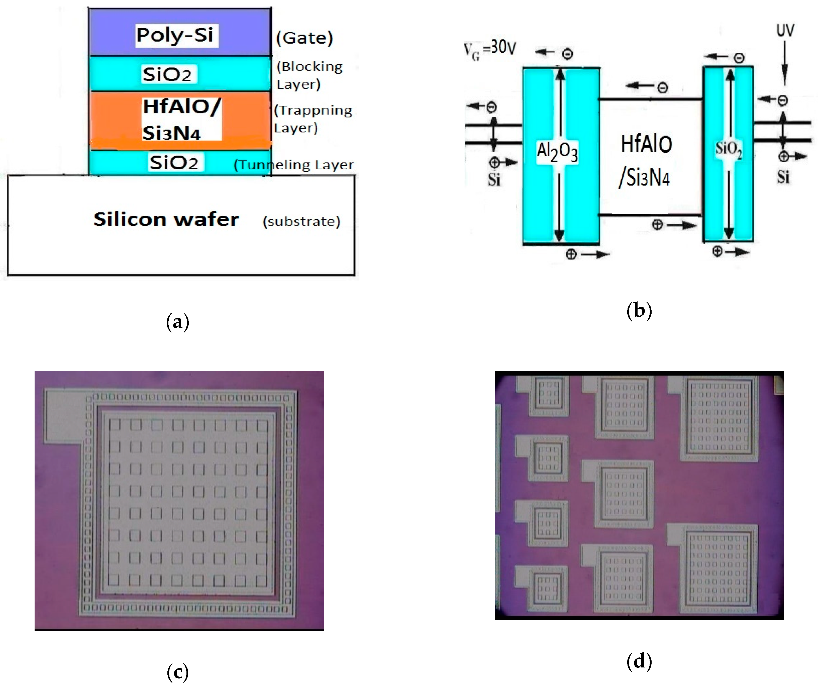
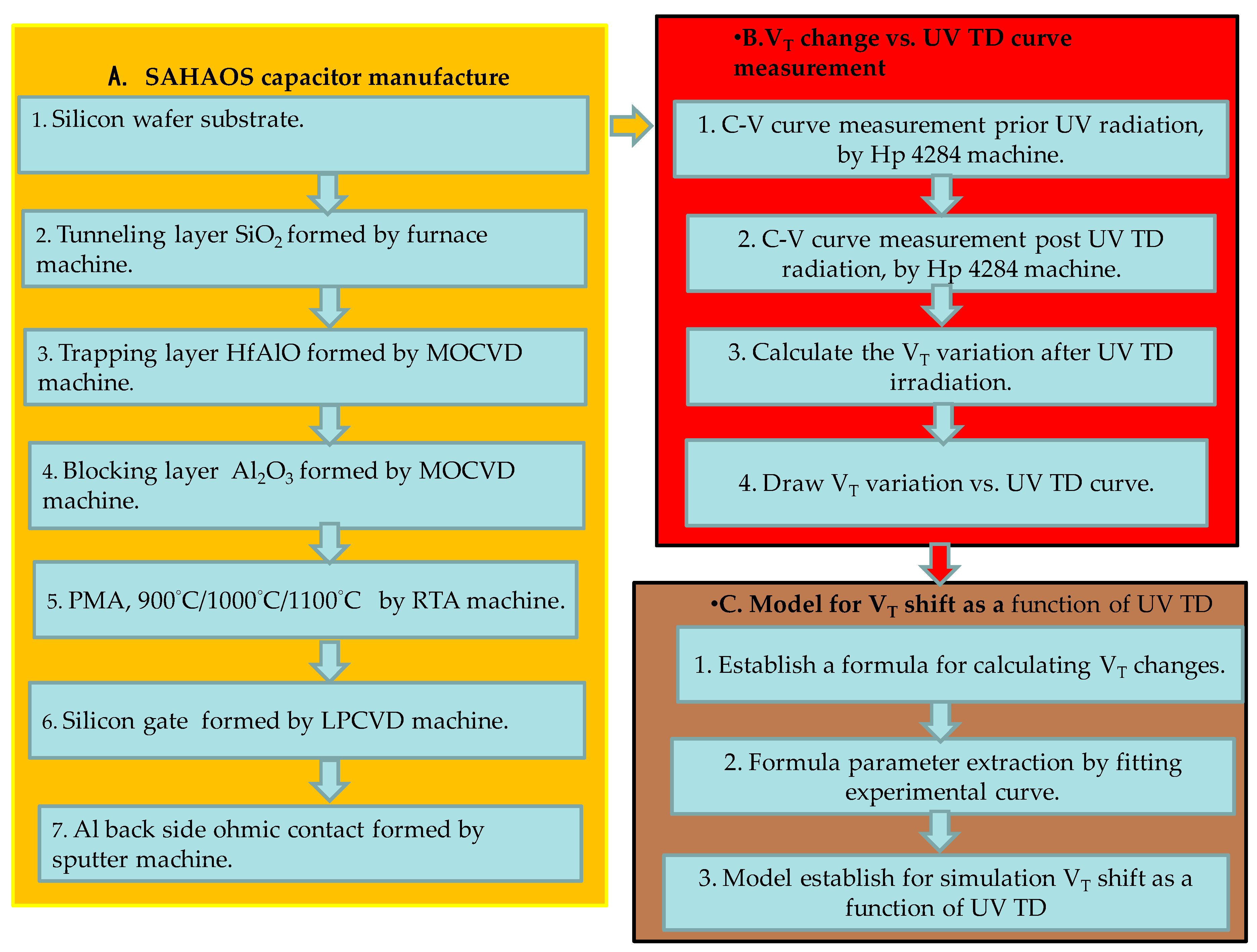
2.1. Sensor Fabrication
2.2. Sensor Fabrication
2.3. Sensor UV TD Information Measurement
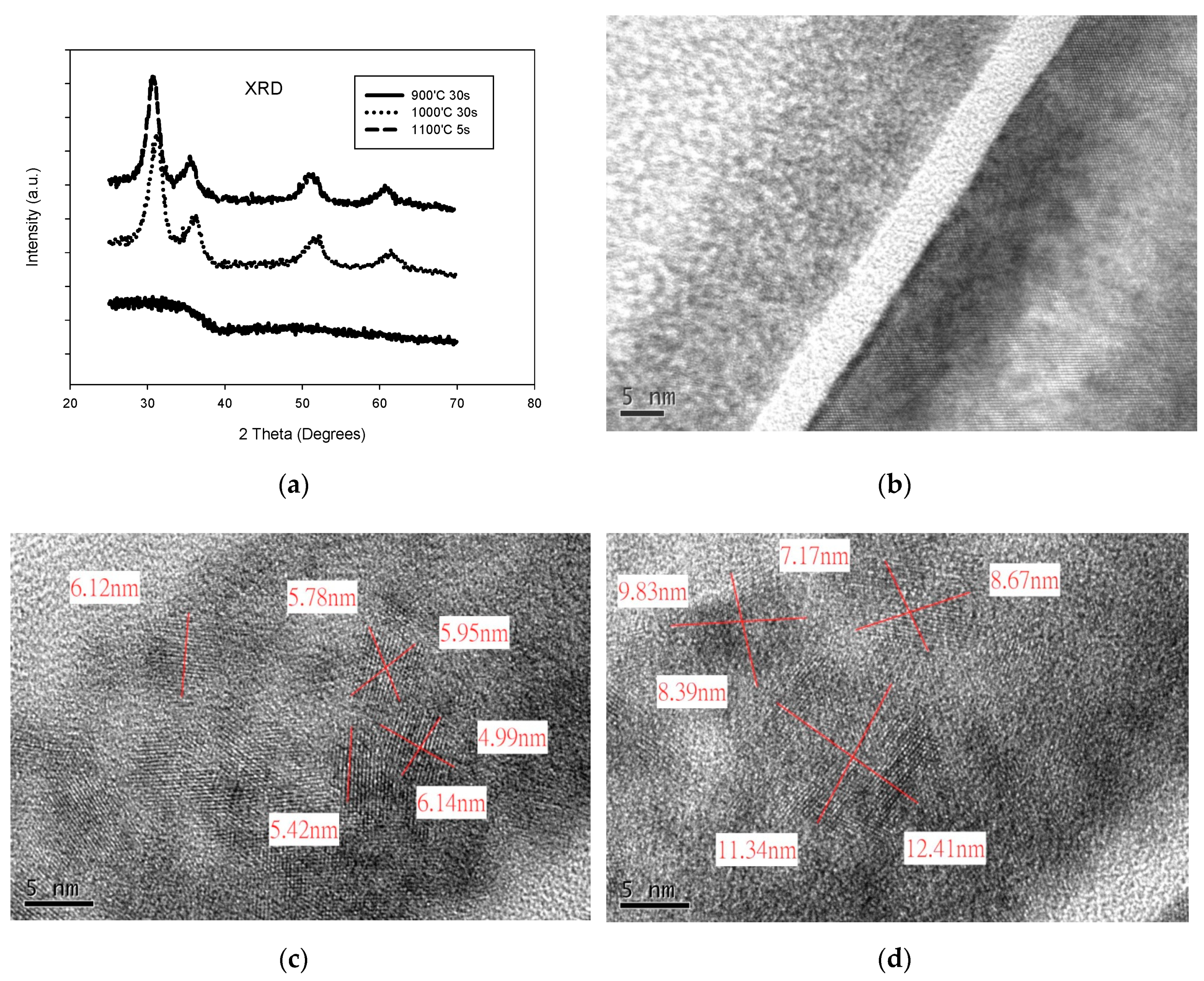
2.4. Sensor Material Analysis
3. Results
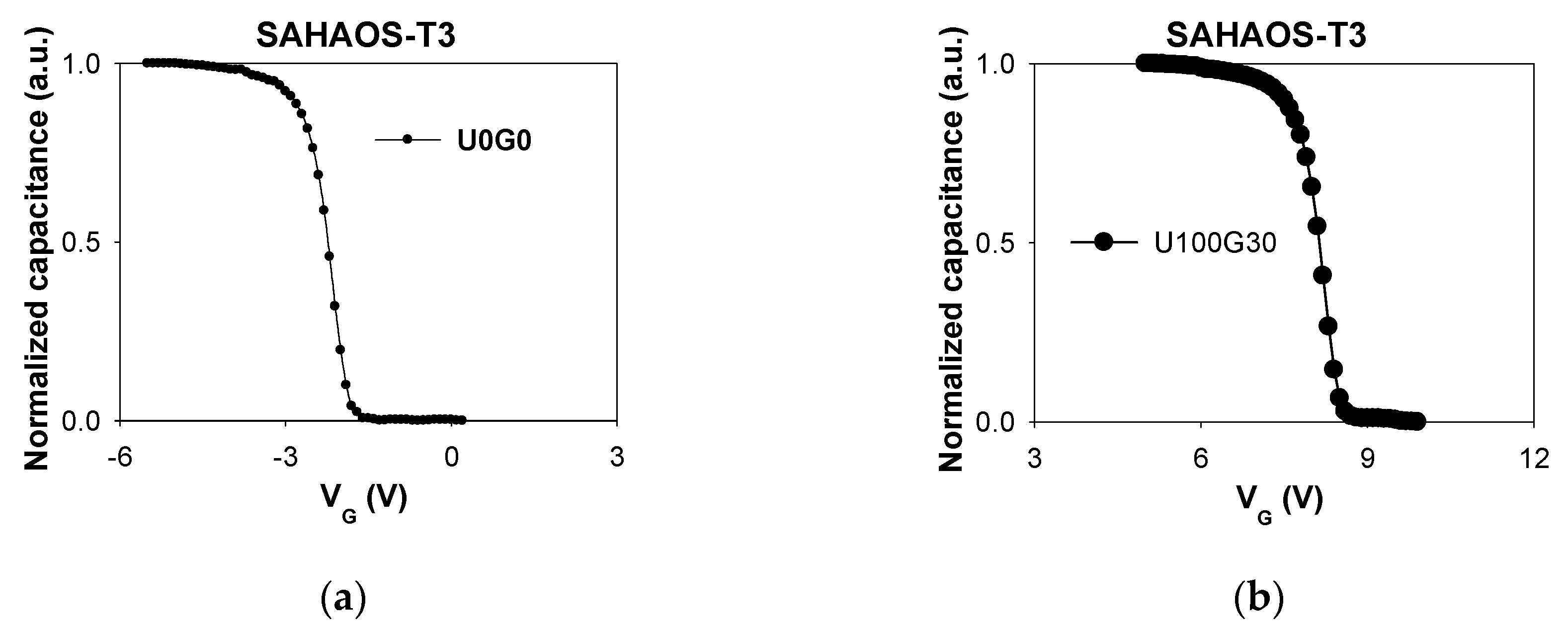
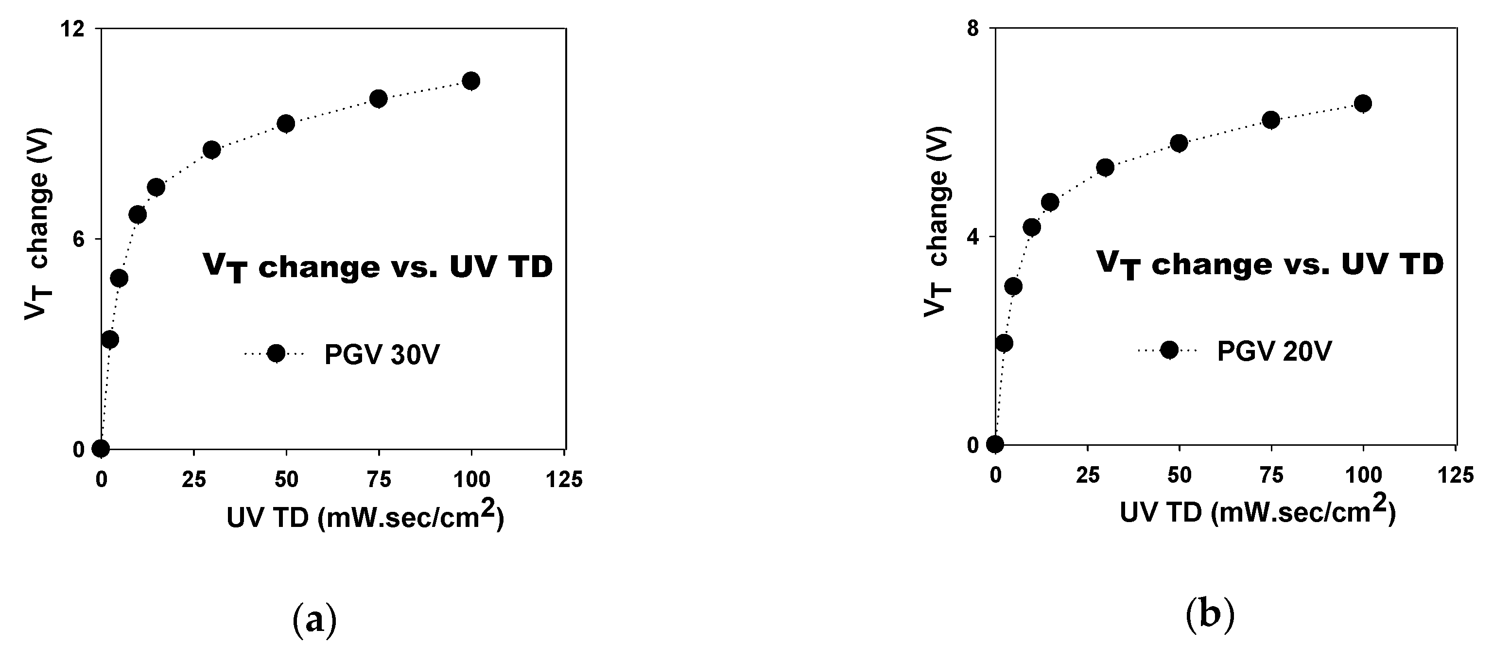
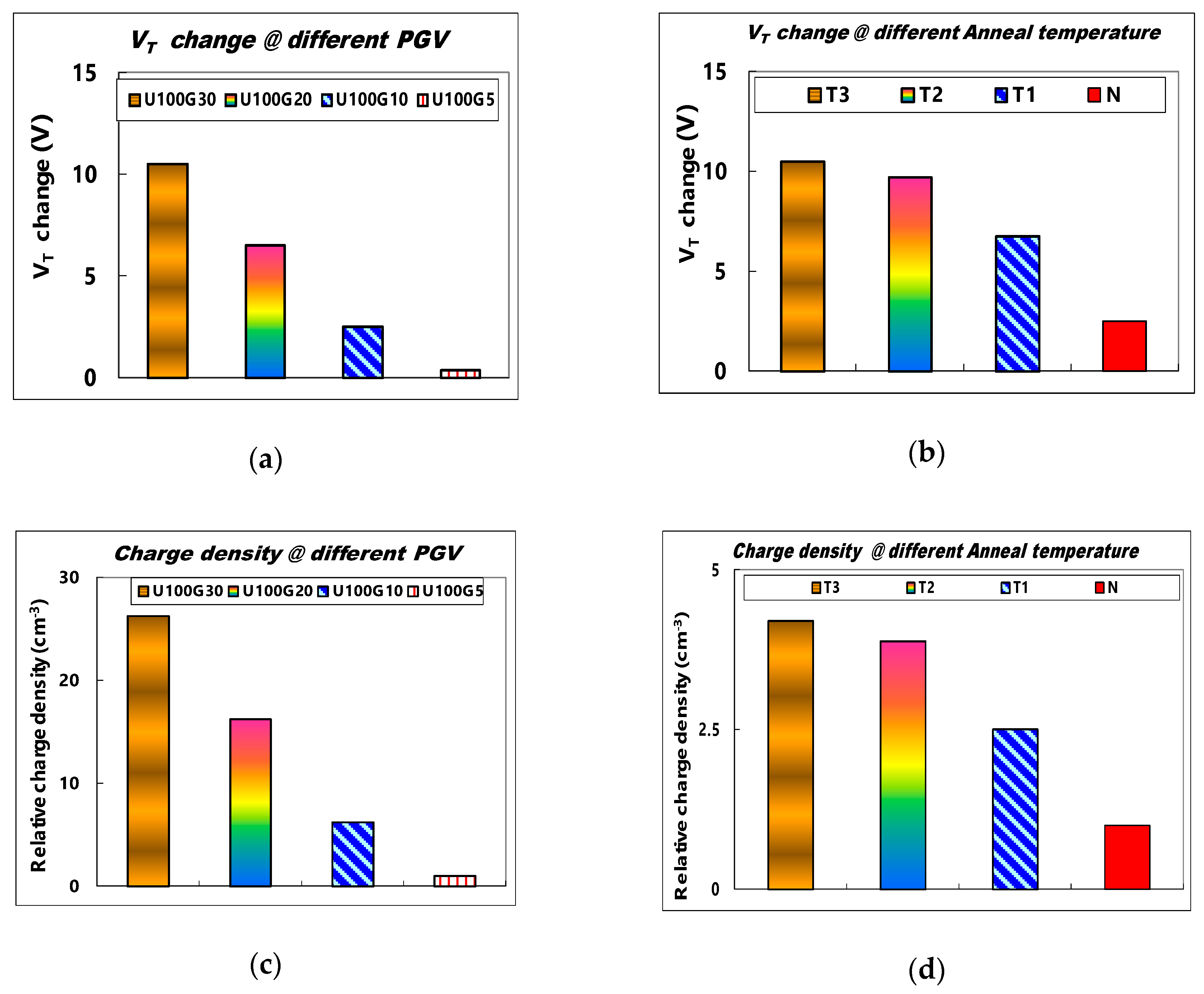
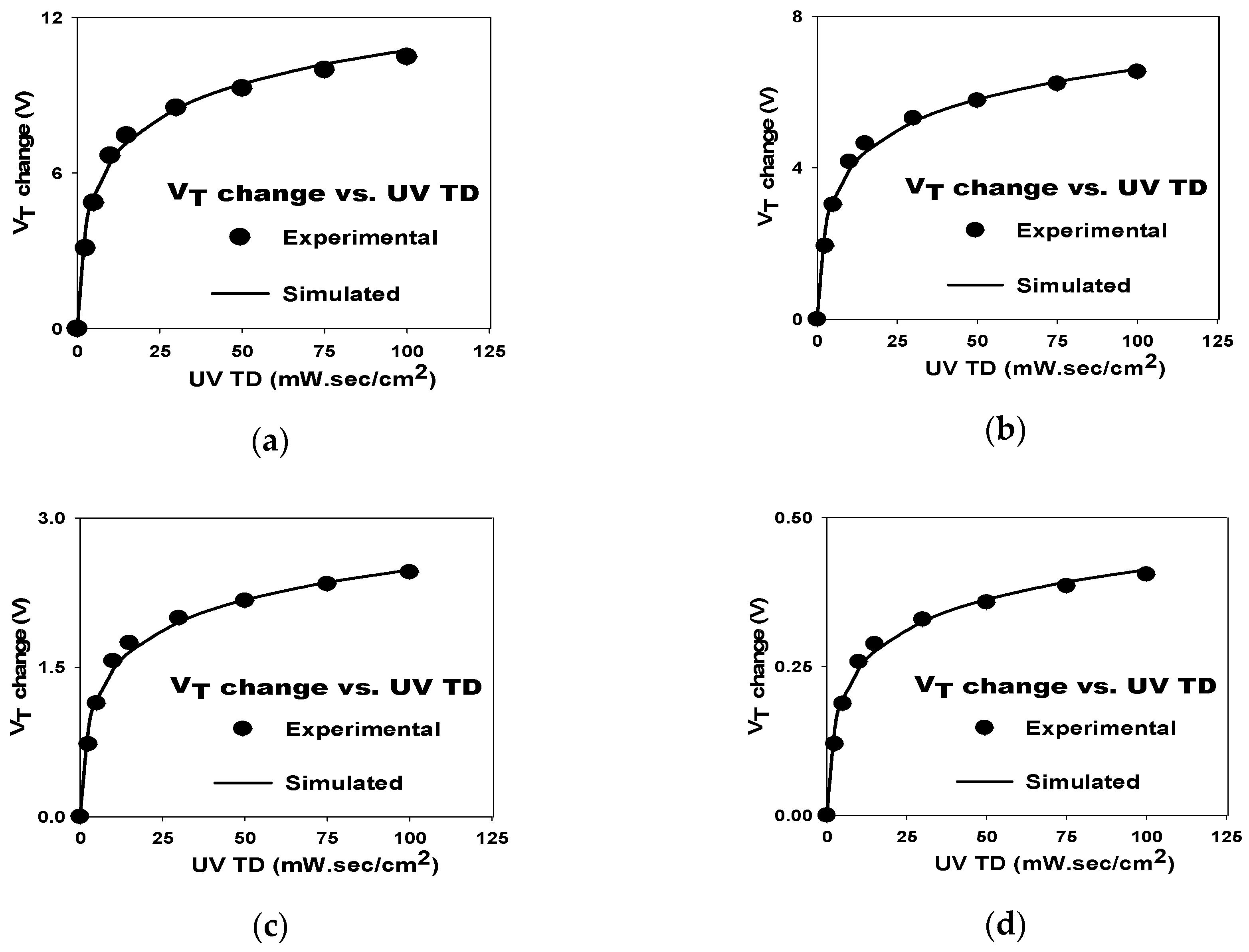
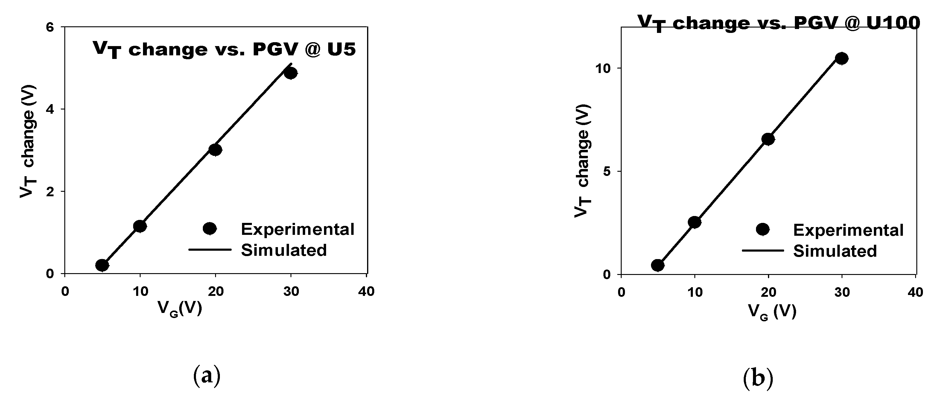
3.1. UV-Induced VT Shift in SAHAOS
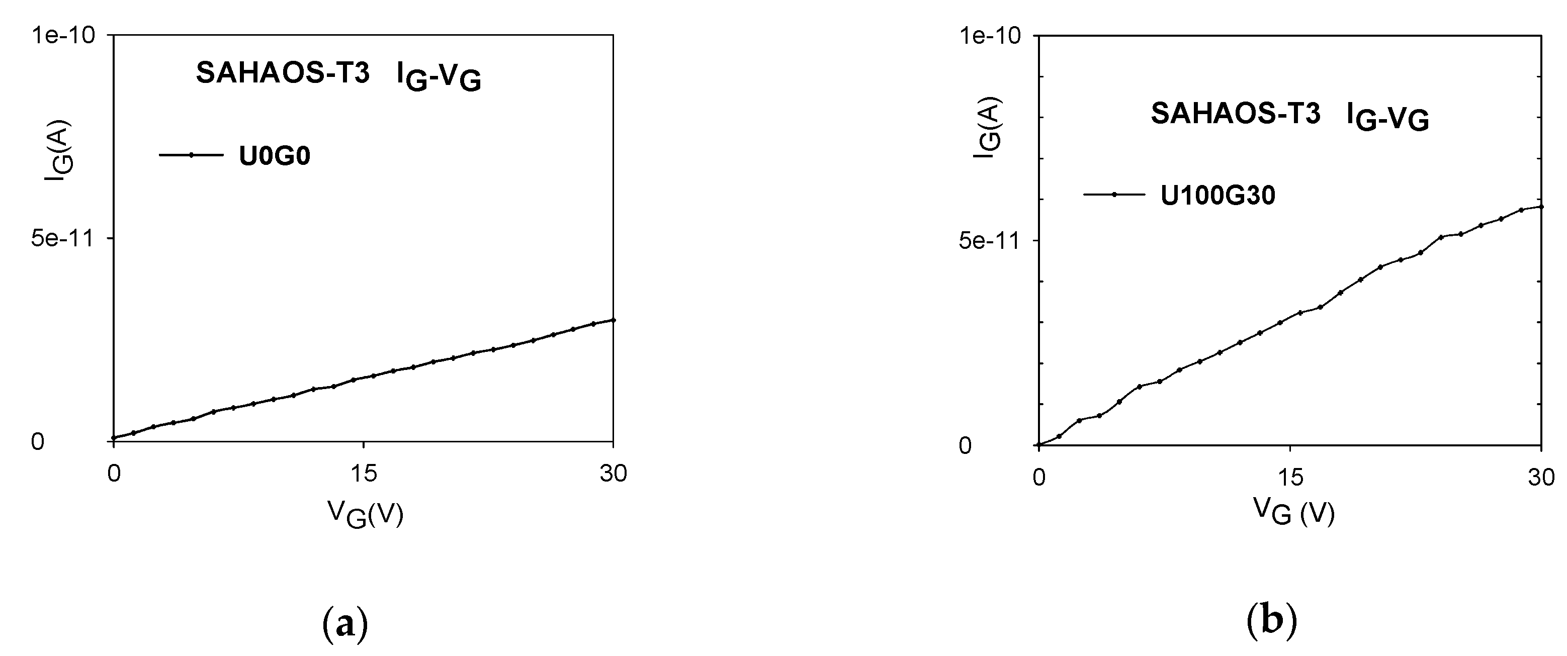
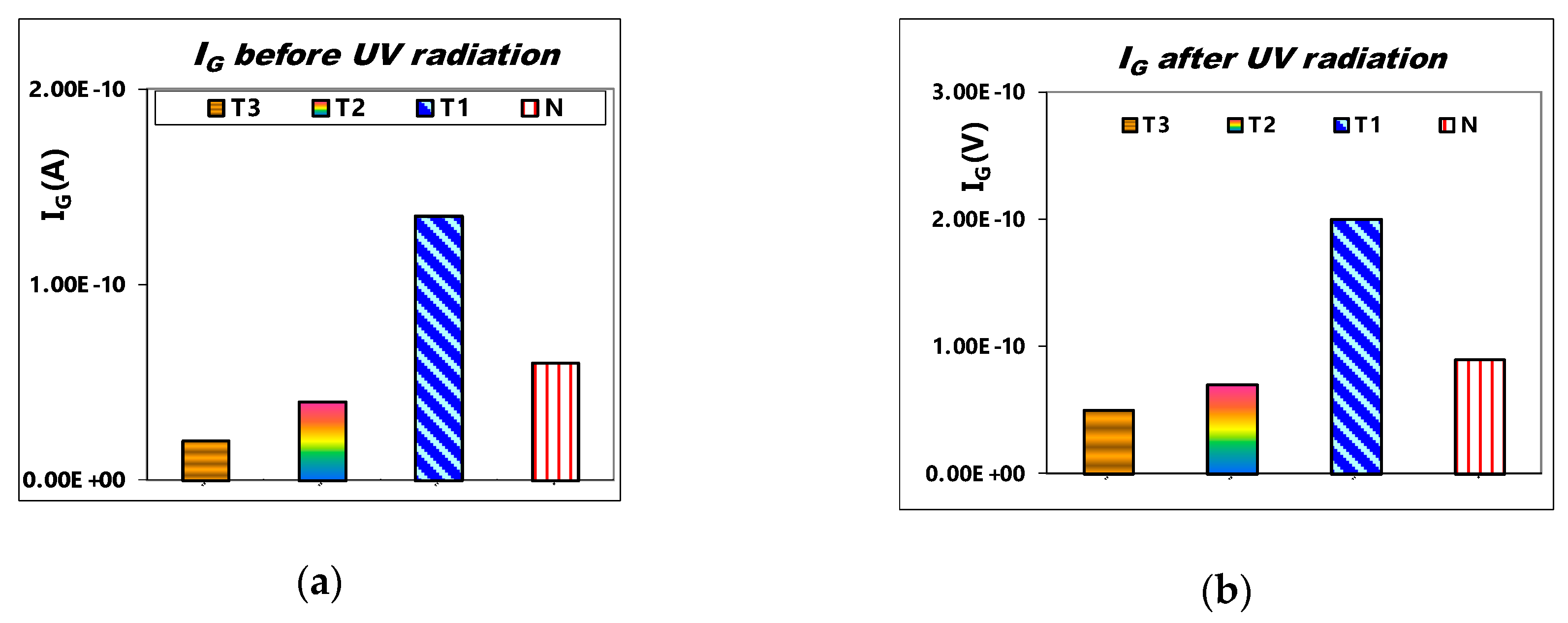
3.2. Gate Leakage Current Comparison
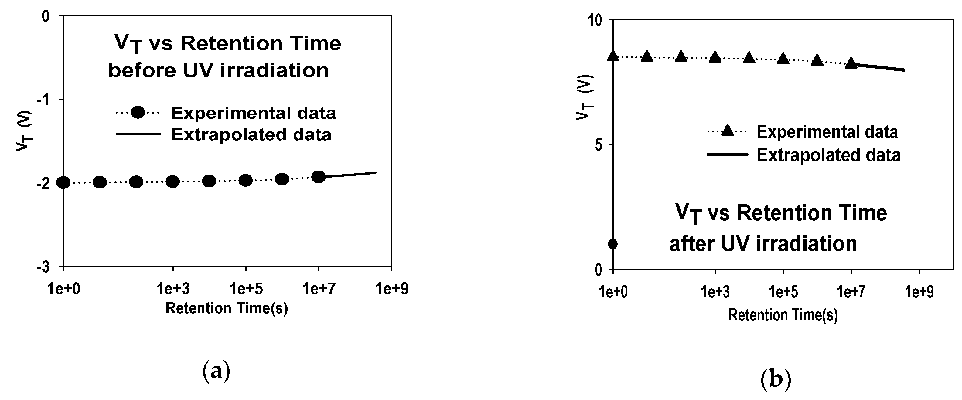
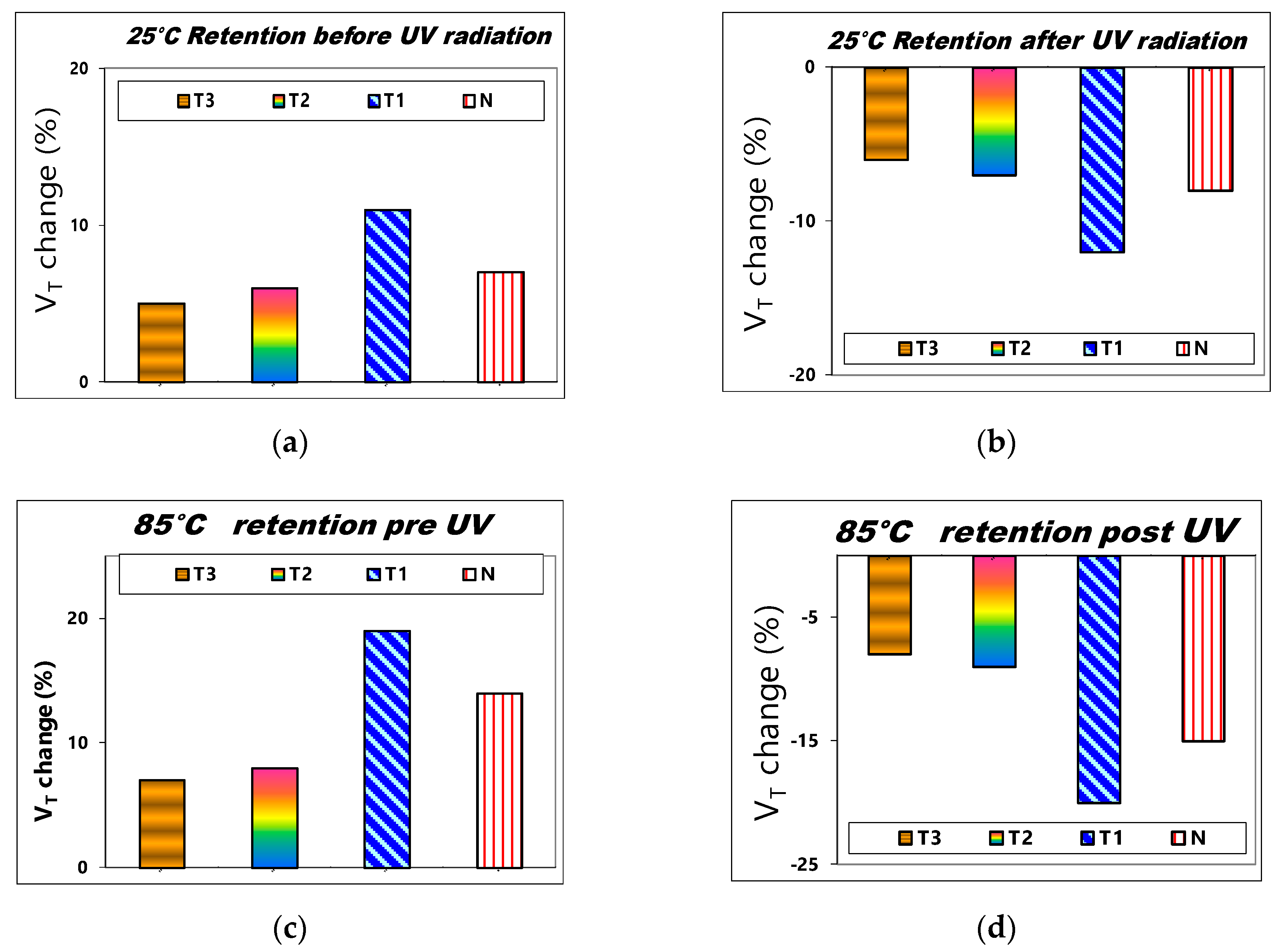
3.3. VT Stability vs. Retention Time
3.4. Model for UV-Induced VT Shift
4. Discussion
4.1. UV-Induced VT Shift in SAHAOS
4.2. Gate Leakage Current Comparison
4.3. VT Stability vs. Retention Time
5. Conclusions
Author Contributions
Funding
Acknowledgments
Conflicts of Interest
References
- Sze, S.M.; Ng, K.K. Physics of Semiconductor Devices, 3rd ed.; John Wiley & Sons: Hoboken, NJ, USA, 2006; p. 663. [Google Scholar]
- Hsieh, W.C.; Su, C.S. UV induced thermoluminescence in ZrO2 doped by Er2O3. J. Phys. D Appl. Phys. 1994, 27, 1763–1768. [Google Scholar] [CrossRef]
- Pejović, M.M. P-channel MOSFET as a sensor and dosimeter of ionizing radiation. Electron. Energ. 2016, 29, 509–541. [Google Scholar] [CrossRef]
- Ho, W.S.; Lin, C.-H.; Kuo, P.-S. Metal Oxide Semiconductor UV Sensor. Proc. IEEE Sens. 2008, 1584–1587. [Google Scholar] [CrossRef]
- Jong, F.C.; Hsieh, W.C.; Lee, H.D.; Wu, S.C. UV Total Dose Nonvolatile Sensor Using Silicon–Oxide–Nitride–Oxide–Silicon Capacitor with Oxy-nitride as Charge-trapping Layer. Sens. Mater. 2018, 30, 1831–1839. [Google Scholar] [CrossRef]
- Hsieh, W.C. UV Total Dose Nonvolatile Sensor Using Fluorine-Treated SOHOS Capacitor Device. Proceedings 2018, 2, 144. [Google Scholar] [CrossRef]
- Oldham, T.R.; McLean, F.B. Total Ionizing Dose Effects in MOS Oxides and Devices. IEEE Trans. Nucl. Sci. 2003, 50, 483–499. [Google Scholar] [CrossRef]
- Tsai, P.H.; Chang-Liao, K.S.; Liu, C.Y.; Wang, T.K.; Tzeng, P.J.; Lin, C.H.; Lee, L.S.; Tsai, M.J. Novel SONOS-Type Nonvolatile Memory Device with Optimal Al Doping in HfAlO Charge-Trapping Layer. IEEE Electron. Device Lett. 2008, 29, 265–268. [Google Scholar] [CrossRef]
- Tan, Y.N.; Chim, W.K.; Choi, W.K.; Joo, M.S.; Ng, T.H.; Cho, B.J. High-K HfAlO Charge Trapping Layer in SONOS-type Nonvolatile Memory Device for High Speed Operation. IEEE IEDM 2004, 04, 889–892. [Google Scholar]
- Yu, H.Y.; Li, M.F.; Kwong, D.L. ALD (HfO2)x(Al2O3)-1x high-k gate dielectrics for advanced MOS devices application. Thin Solid Films 2004, 462, 110–113. [Google Scholar] [CrossRef]
- Zhu, W.J.; Tamagawa, T.; Gibson, M.; Furukawa, T.; Ma, T.P. Effect of Al Inclusion in HfO2 on the Physical and Electrical Properties of the Dielectrics. IEEE Electr. Device Lett. 2002, 23, 649–651. [Google Scholar] [CrossRef]
- Tan, Y.N.; Chim, W.K.; Choi, W.K.; Joo, M.S.; Cho, B.J. Hafnium Aluminum Oxide as Charge Storage and Blocking-Oxide Layers in SONOS-Type Nonvolatile Memory for High-Speed Operation. IEEE Trans. Electron. Devices 2006, 53, 654–662. [Google Scholar] [CrossRef]
- Zhu, W.; Ma, T.P.; Tamagawa, T.; Di, Y.; Kim, J.; Carmthers, R.; Gibson, M.; Furukawa, T. HfO2 and HfAlO for CMOS: Thermal Stability and Current Transport. IEEE IEDM 2001, 1, 463–466. [Google Scholar]
- Hsieh, W.C.; Lee, H.D.; Jong, F.C. An Ionizing Radiation Sensor Using a Pre-Programmed MAHAOS Device. Sensors 2014, 14, 14553–14566. [Google Scholar] [CrossRef]
- Zhang, G.; Samanta, S.K.; Singh, P.K.; Ma, F.J.; Yoo, M.T.; Roh, Y.; Yoo, W.J. Partial Crystallization of HfO2 for Two-Bit/Four-Level SONOS-Type Flash Memory. IEEE Trans. Electron. Devices 2007, 54, 3177–3185. [Google Scholar] [CrossRef]
- Lin, Y.H.; Chien, C.H.; Chang, C.Y.; Lei, T.F. Annealing temperature effect on the performance of nonvolatile HfO2 Si–oxide–nitride–oxide–silicon–type flash memory. J. Vac. Sci. Technol. A Vac. Surf. Films 2006, 24, 682–685. [Google Scholar] [CrossRef]
- Wakai, H.; Sugizaki, T.; Kumise, T.; Kobayashi, M.; Yamaguchi, M.; Nakanishi, T.; Tanaka, H. Ultra high density HfO2-nanodot memory for flash memory scaling. Jpn. J. Appl. Phys. 2005, 45, 2459–2462. [Google Scholar] [CrossRef]
- Banerjee, W.; Maikap, S. High-κ Hf-based Nanocrystal Memory Capacitors with IrOx Metal Gate for NAND Application. In Proceedings of the 2009 IEEE International Workshop on Memory Technology, Design and Testing, Hsinchu, Taiwan, 31 August–2 September 2009. [Google Scholar]
- Lin, Y.H.; Chien, C.H.; Lin, C.T.; Chang, C.Y. Novel Two-Bit HfO2 Nanocrystal Nonvolatile Flash Memory. IEEE Trans. Electron Devices 2006, 53, 782–789. [Google Scholar]
- Sivasubramani, P.; Kim, J.; Kim, M.J.; Gnade, B.E.; Wallace, R.M. Effect of composition on the thermal stability of sputter deposited hafnium aluminate and nitrided hafnium aluminate dielectrics on Si (100). J. Appl. Phys. 2007, 101, 114108. [Google Scholar] [CrossRef]


| Sensor Device Abbreviation | Device Materials Composition | Characterization | Reference |
|---|---|---|---|
| PIN | SiC | Cannot measure UV TD, only can measure UV intensity | [1] Sze, S.M. 2006. |
| TLD | Er2O3 doped ZrO2 | UV TD record is not easily readable | [2] Hsien, W.C. 1994. |
| MOS | Si-SiO2-Si | Stability with time after irradiation is very bad | [3] Pejović, M.M. 2016. [4] Ho, W.S. 2008. |
| SONOS | O doped Si-SiO2-Si3N4-SiO2-Si | Sensitivity to irradiation and stability with time after irradiation can been improved | [5] Jong, F.C. 2018. |
| F-SOHOS | F doped Si-SiO2-HfO2-SiO2-Si | Sensitivity to irradiation and stability with time after irradiation can been improved | [6] Hsien, W.C. 2018. |
| PNC-SAHAOS | 1000 °C/1100 °C PMA Si-Al2O3-HfAlO-SiO2-Si | Sensitivity to irradiation and stability with time after irradiation are very good | This paper. |
| Split | T1 | T2 | T3 | N |
|---|---|---|---|---|
| PMA temperature (°C) | 900 | 1000 | 1100 | 900 |
| PMA time (s) | 30 | 30 | 5 | 30 |
| Trapping Layer | HfAlO | HfAlO | HfAlO | Si3N4 |
| Symbol | UV TD (mW·s/cm2) | PGV (V) |
|---|---|---|
| U0G0 | 0 mW·s/cm2 | 0 V |
| U100G5 | 100 mW·s/cm2 | 5 V |
| U100G10 | 100 mW·s/cm2 | 10 V |
| U100G20 | 100 mW·s/cm2 | 20 V |
| U100G30 | 100 mW·s/cm2 | 30 V |
© 2019 by the author. Licensee MDPI, Basel, Switzerland. This article is an open access article distributed under the terms and conditions of the Creative Commons Attribution (CC BY) license (http://creativecommons.org/licenses/by/4.0/).
Share and Cite
Hsieh, W.-C. Performance Improvement of a Nonvolatile UV TD Sensor Using SAHAOS with a High Temperature Annealed, Partially Nano-Crystallized Trapping Layer. Sensors 2019, 19, 1570. https://doi.org/10.3390/s19071570
Hsieh W-C. Performance Improvement of a Nonvolatile UV TD Sensor Using SAHAOS with a High Temperature Annealed, Partially Nano-Crystallized Trapping Layer. Sensors. 2019; 19(7):1570. https://doi.org/10.3390/s19071570
Chicago/Turabian StyleHsieh, Wen-Ching. 2019. "Performance Improvement of a Nonvolatile UV TD Sensor Using SAHAOS with a High Temperature Annealed, Partially Nano-Crystallized Trapping Layer" Sensors 19, no. 7: 1570. https://doi.org/10.3390/s19071570
APA StyleHsieh, W.-C. (2019). Performance Improvement of a Nonvolatile UV TD Sensor Using SAHAOS with a High Temperature Annealed, Partially Nano-Crystallized Trapping Layer. Sensors, 19(7), 1570. https://doi.org/10.3390/s19071570