Recent Progress on Non-Conventional Microfabricated Probes for the Chronic Recording of Cortical Neural Activity


Abstract
:1. Introduction
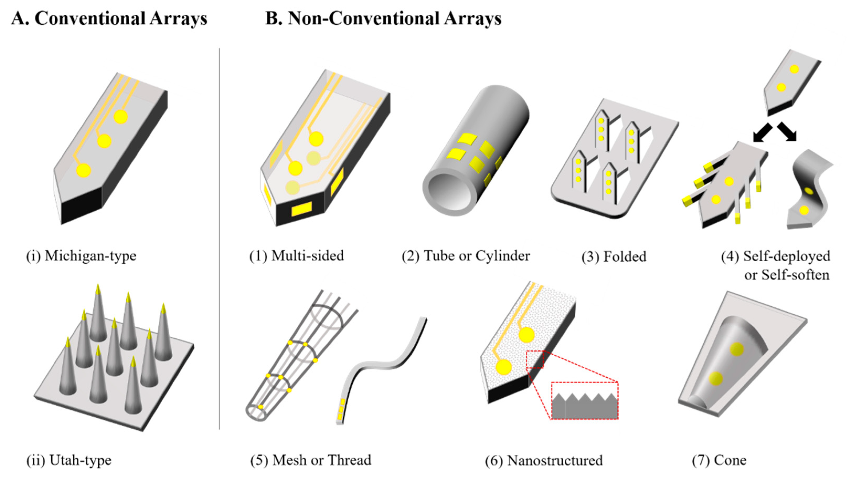
2. Non-Conventional Neural Probes
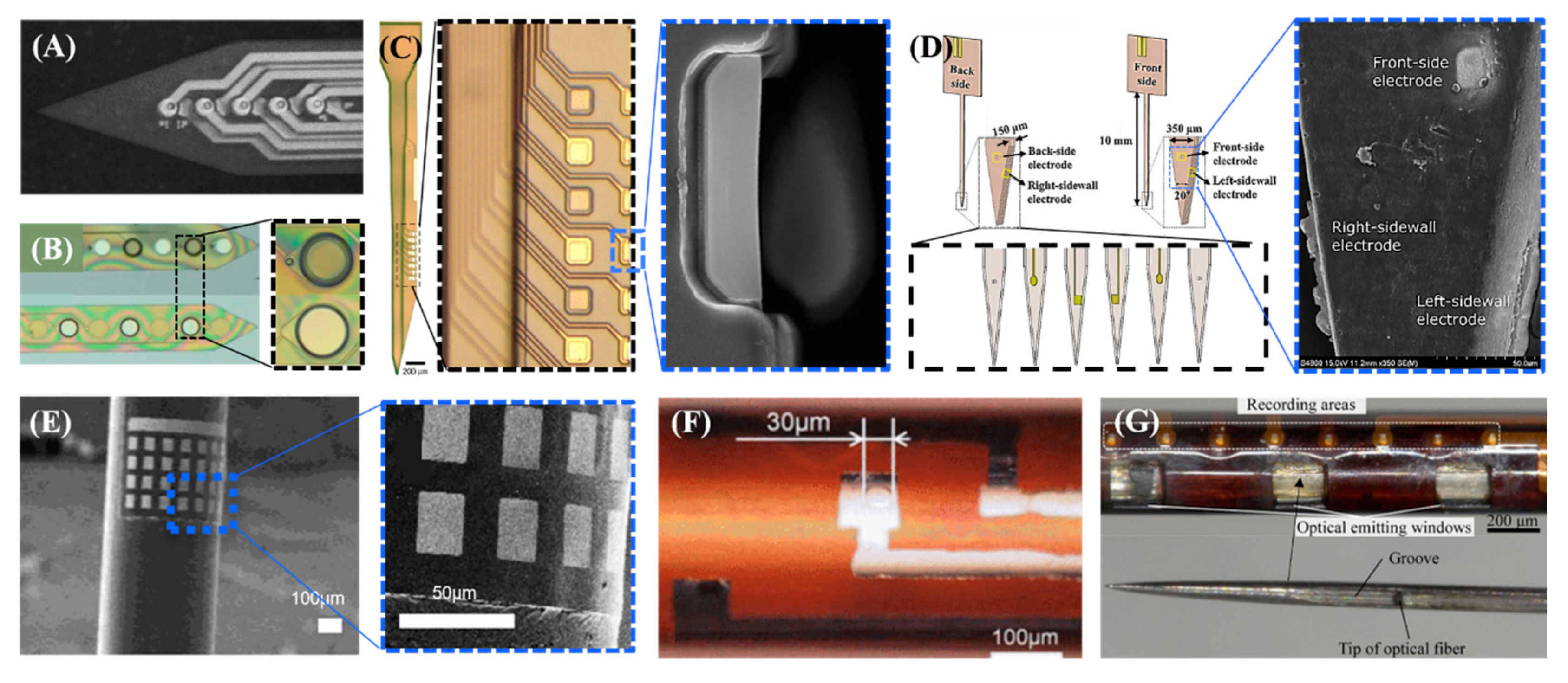
2.1. Multi-Sided Probes
2.2. Tubular or Cylindrical Probes
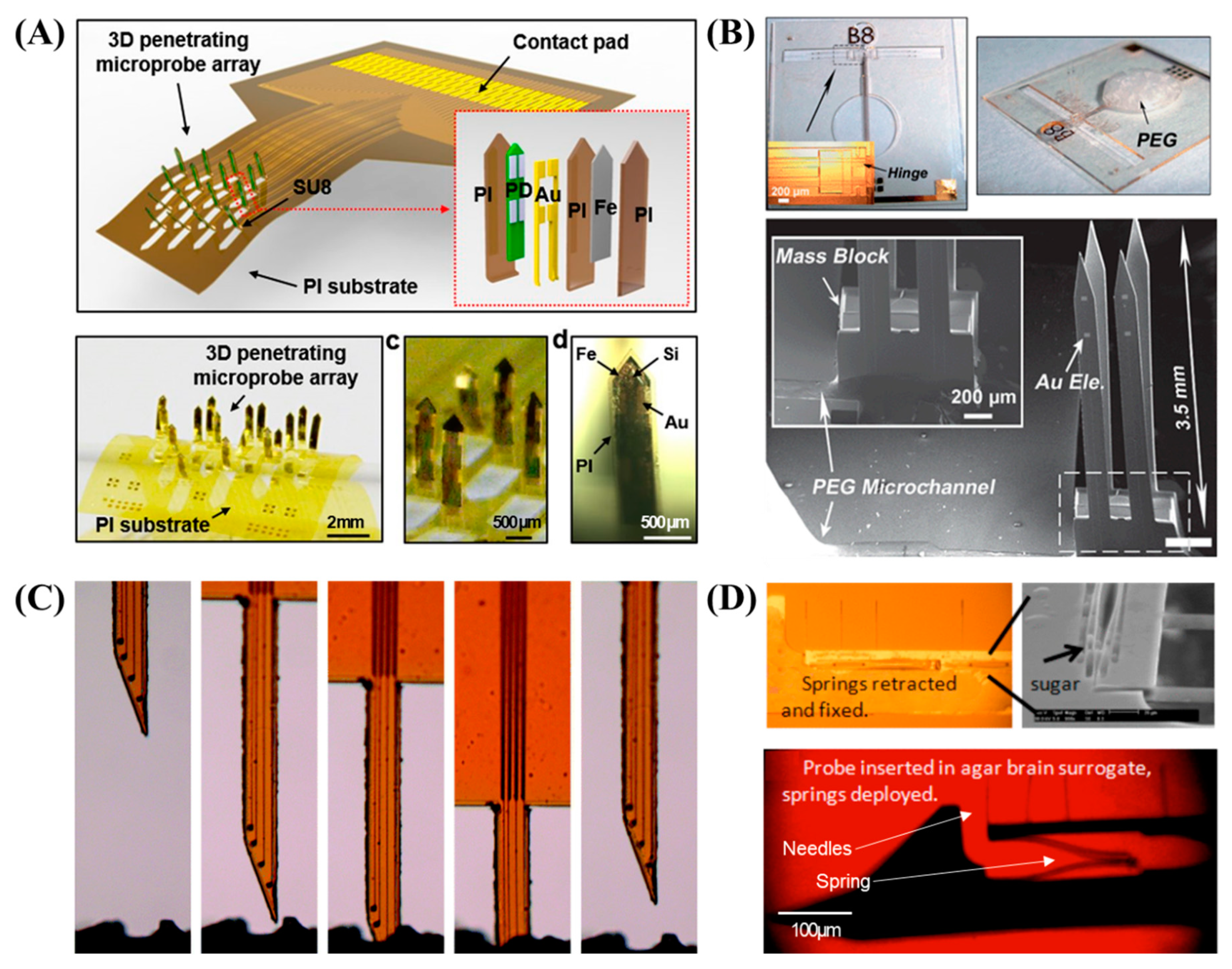
2.3. Folded Probes
2.4. Mechanically Dynamic Probes (Self-Softening or Self-Deploying Probes)
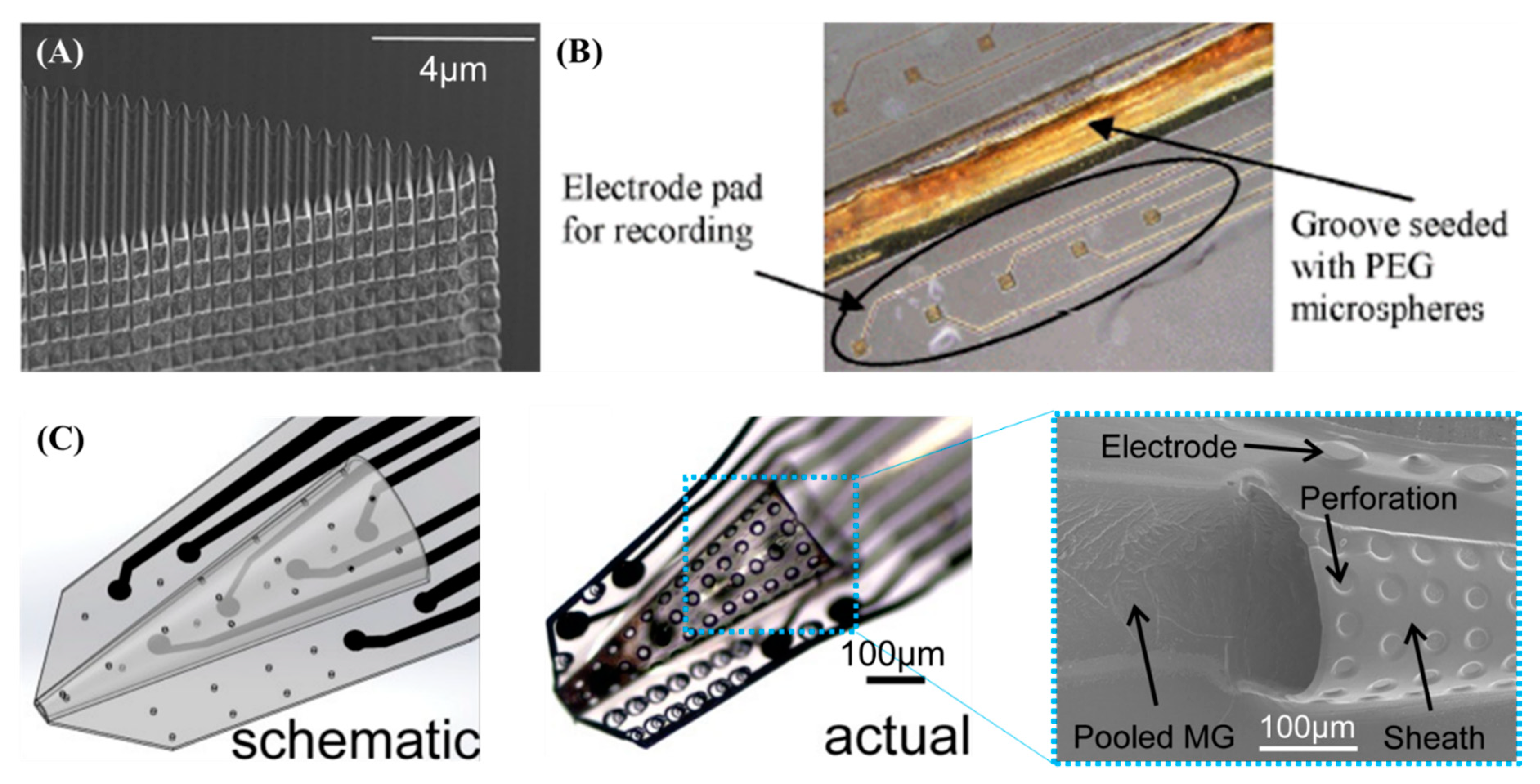
2.5. Mesh and Thread Probes
2.6. Nano-Structured Probes
2.7. Sheath Probes
3. Conclusions and Perspectives
Author Contributions
Funding
Conflicts of Interest
References
- Fiáth, R.; Raducanu, B.C.; Musa, S.; Andrei, A.; Lopez, C.M.; van Hoof, C.; Ruther, P.; Aarts, A.; Horváth, D.; Ulbert, I. A silicon-based neural probe with densely-packed low-impedance titanium nitride microelectrodes for ultrahigh-resolution in vivo recordings. Biosens. Bioelectron. 2018, 106, 86–92. [Google Scholar] [CrossRef] [PubMed]
- Lanzio, V.; West, M.; Koshelev, A.; Telian, G.; Micheletti, P.; Lambert, R.; Dhuey, S.; Adesnik, H.; Sassolini, S.; Cabrini, S. High-density electrical and optical probes for neural readout and light focusing in deep brain tissue. J. Micro Nanolithogr. MEMS MOEMS 2018, 17, 025503. [Google Scholar] [CrossRef]
- Scholten, K.; Meng, E. Electron-beam lithography for polymer bioMEMS with submicron features. Microsyst. Nanoeng. 2016, 2, 16053. [Google Scholar] [CrossRef]
- Rios, G.; Lubenov, E.V.; Chi, D.; Roukes, M.L.; Siapas, A.G. Nanofabricated neural probes for dense 3-D recordings of brain activity. Nano Lett. 2016, 16, 6857–6862. [Google Scholar] [CrossRef] [PubMed]
- Scholvin, J.; Kinney, J.P.; Bernstein, J.G.; Moore-Kochlacs, C.; Kopell, N.; Fonstad, C.G.; Boyden, E.S. Close-Packed Silicon Microelectrodes for Scalable Spatially Oversampled Neural Recording. IEEE Trans. Biomed. Eng. 2016, 63, 120–130. [Google Scholar] [CrossRef] [PubMed]
- Cheung, K.; Gun, L.; Djupsund, K.; Yang, D.; Lee, L.P. A new neural probe using SOI wafers with topological interlocking mechanisms. In Proceedings of the 1st Annual International IEEE-EMBS Special Topic Conference on Microtechnologies in Medicine and Biology, Lyon, France, 12–14 October 2000; pp. 507–511. [Google Scholar]
- Jeong, J.; Bae, S.H.; Min, K.S.; Seo, J.M.; Chung, H.; Kim, S.J. A Miniaturized, Eye-conformable, and Long-term Reliable Retinal Prosthesis using Monolithic Fabrication of Liquid Crystal Polymer (LCP). IEEE Trans. Biomed. Eng. 2015, 62, 982–989. [Google Scholar] [CrossRef] [PubMed]
- Kim, B.J.; Meng, E. Micromachining of Parylene C for bioMEMS. Polym. Adv. Technol. 2016, 27, 564–576. [Google Scholar] [CrossRef]
- Kim, G.; Kim, K.; Lee, E.; An, T.; Choi, W.; Lim, G.; Shin, J. Recent Progress on Microelectrodes in Neural Interfaces. Materials (Basel) 2018, 11, 1995. [Google Scholar] [CrossRef] [PubMed]
- Kindlundh, M.; Norlin, P.; Hofmann, U.G. A neural probe process enabling variable electrode configurations. Sens. Actuators B Chem. 2004, 102, 51–58. [Google Scholar] [CrossRef]
- Hajj-Hassan, M.; Chodavarapu, V.; Musallam, S. Microfabrication of ultra-long reinforced silicon neural electrodes. Micro Nano Lett. 2009, 4, 53–58. [Google Scholar] [CrossRef]
- Iseri, E.; Kuzum, D. Implantable optoelectronic probes for in vivo optogenetics. J. Neural Eng. 2017, 14, 031001. [Google Scholar] [CrossRef] [PubMed]
- Rivnay, J.; Wang, H.; Fenno, L.; Deisseroth, K.; Malliaras, G.G. Next-generation probes, particles, and proteins for neural interfacing. Sci. Adv. 2017, 3, 1–20. [Google Scholar] [CrossRef] [PubMed]
- Johnson, M.D.; Franklin, R.K.; Gibson, M.D.; Brown, R.B.; Kipke, D.R. Implantable microelectrode arrays for simultaneous electrophysiological and neurochemical recordings. J. Neurosci. Methods 2008, 174, 62–70. [Google Scholar] [CrossRef] [PubMed]
- Neves, H.P.; Orban, G.A.; Koudelka-Hep, M.; Stieglitz, T.; Ruther, P. Development of Modular Multifunctional Probe Arrays for Cerebral Applications. In Proceedings of the 2007 3rd International IEEE/EMBS Conference on Neural Engineering, Kohala Coast, HI, USA, 2–5 May 2007; pp. 104–109. [Google Scholar]
- Ximiao, W.; Tingyi, L.; Pei-Yu, C. A hybrid silicon-PDMS multifunctional neural probe. In Proceedings of the 2016 International Conference on Optical MEMS and Nanophotonics (OMN), Singapore, 31 July–4 August 2016; pp. 1–2. [Google Scholar]
- De Dorigo, D.; Moranz, C.; Graf, H.; Marx, M.; Wendler, D.; Shui, B.; Herbawi, A.S.; Kuhl, M.; Ruther, P.; Paul, O. Fully Immersible Subcortical Neural Probes With Modular Architecture and a Delta-Sigma ADC Integrated Under Each Electrode for Parallel Readout of 144 Recording Sites. IEEE J. Solid-State Circuits 2018, 53, 3111–3125. [Google Scholar] [CrossRef]
- Herbawi, A.S.; Christ, O.; Kiessner, L.; Mottaghi, S.; Hofmann, U.G.; Paul, O.; Ruther, P. CMOS Neural Probe With 1600 Close-Packed Recording Sites and 32 Analog Output Channels. J. Microelectromech. Syst. 2018, 27, 1023–1034. [Google Scholar] [CrossRef]
- Jun, J.J.; Steinmetz, N.A.; Siegle, J.H.; Denman, D.J.; Bauza, M.; Barbarits, B.; Lee, A.K.; Anastassiou, C.A.; Andrei, A.; Aydın, Ç. Fully integrated silicon probes for high-density recording of neural activity. Nature 2017, 551, 232–236. [Google Scholar] [CrossRef] [PubMed]
- Lopez, C.M.; Andrei, A.; Mitra, S.; Welkenhuysen, M.; Eberle, W.; Bartic, C.; Puers, R.; Yazicioglu, R.F.; Gielen, G.G. An implantable 455-active-electrode 52-channel CMOS neural probe. IEEE J. Solid-State Circuits 2014, 49, 248–261. [Google Scholar] [CrossRef]
- Raducanu, B.C.; Yazicioglu, R.F.; Lopez, C.M.; Ballini, M.; Putzeys, J.; Wang, S.; Andrei, A.; Rochus, V.; Welkenhuysen, M.; Helleputte, N.V. Time multiplexed active neural probe with 1356 parallel recording sites. Sensors 2017, 17, 2388. [Google Scholar] [CrossRef] [PubMed]
- Steinmetz, N.A.; Koch, C.; Harris, K.D.; Carandini, M. Challenges and opportunities for large-scale electrophysiology with Neuropixels probes. Curr. Opin. Neurobiol. 2018, 50, 92–100. [Google Scholar] [CrossRef] [PubMed]
- Wise, K.D.; Sodagar, A.M.; Yao, Y.; Gulari, M.N.; Perlin, G.E.; Najafi, K. Microelectrodes, microelectronics, and implantable neural microsystems. Proc. IEEE 2008, 96, 1184–1202. [Google Scholar] [CrossRef]
- Patterson, W.R.; Yoon-Kyu, S.; Bull, C.W.; Ozden, I.; Deangellis, A.P.; Lay, C.; McKay, J.L.; Nurmikko, A.V.; Donoghue, J.D.; Connors, B.W. A microelectrode/microelectronic hybrid device for brain implantable neuroprosthesis applications. IEEE Trans. Biomed. Eng. 2004, 51, 1845–1853. [Google Scholar] [CrossRef] [PubMed]
- Song, Y.-K.; Patterson, W.R.; Bull, C.W.; Beals, J.; Hwang, N.; Deangelis, A.P.; Lay, C.; McKay, J.L.; Nurmikko, A.V.; Fellows, M.R. Development of a chipscale integrated microelectrode/microelectronic device for brain implantable neuroengineering applications. IEEE Trans. Neural Syst. Rehabil. Eng. 2005, 13, 220–226. [Google Scholar] [CrossRef] [PubMed]
- Goncalves, S.; Ribeiro, J.; Silva, A.; Costa, R.; Correia, J. Design and manufacturing challenges of optogenetic neural interfaces: A review. J. Neural Eng. 2017, 14, 041001. [Google Scholar] [CrossRef] [PubMed]
- Rudmann, L.; Alt, M.; Vajari, D.A.; Stieglitz, T. Integrated optoelectronic microprobes. Curr. Opin. Neurobiol. 2018, 50, 72–82. [Google Scholar] [CrossRef] [PubMed]
- Royer, S.; Zemelman, B.V.; Barbic, M.; Losonczy, A.; Buzsáki, G.; Magee, J.C. Multi-array silicon probes with integrated optical fibers: Light-assisted perturbation and recording of local neural circuits in the behaving animal. Eur. J. Neurosci. 2010, 31, 2279–2291. [Google Scholar] [CrossRef] [PubMed]
- Zhang, J.; Laiwalla, F.; Kim, J.A.; Urabe, H.; Van Wagenen, R.; Song, Y.-K.; Connors, B.W.; Zhang, F.; Deisseroth, K.; Nurmikko, A.V. Integrated device for optical stimulation and spatiotemporal electrical recording of neural activity in light-sensitized brain tissue. J. Neural Eng. 2009, 6, 055007. [Google Scholar] [CrossRef] [PubMed]
- Stark, E.; Koos, T.; Buzsáki, G. Diode probes for spatiotemporal optical control of multiple neurons in freely moving animals. J. Neurophysiol. 2012, 108, 349–363. [Google Scholar] [CrossRef] [PubMed]
- Wang, J.; Wagner, F.; Borton, D.A.; Zhang, J.; Ozden, I.; Burwell, R.D.; Nurmikko, A.V.; van Wagenen, R.; Diester, I.; Deisseroth, K. Integrated device for combined optical neuromodulation and electrical recording for chronic in vivo applications. J. Neural Eng. 2011, 9, 016001. [Google Scholar] [CrossRef] [PubMed]
- Ozden, I.; Wang, J.; Lu, Y.; May, T.; Lee, J.; Goo, W.; O’Shea, D.J.; Kalanithi, P.; Diester, I.; Diagne, M.; et al. A coaxial optrode as multifunction write-read probe for optogenetic studies in non-human primates. J. Neurosci. Methods 2013, 219, 142–154. [Google Scholar] [CrossRef] [PubMed]
- Kwon, K.Y.; Sirowatka, B.; Weber, A.; Li, W. Opto-μECoG array: A hybrid neural interface with transparent μECoG electrode array and integrated LEDs for optogenetics. IEEE Trans. Biomed. Circuits Syst. 2013, 7, 593–600. [Google Scholar] [CrossRef] [PubMed]
- Zhang, J.; Liu, X.; Xu, W.; Luo, W.; Li, M.; Chu, F.; Xu, L.; Cao, A.; Guan, J.; Tang, S.; et al. Stretchable Transparent Electrode Arrays for Simultaneous Electrical and Optical Interrogation of Neural Circuits in Vivo. Nano Lett. 2018, 18, 2903–2911. [Google Scholar] [CrossRef] [PubMed]
- Sim, J.Y.; Haney, M.P.; Park, S.I.; McCall, J.G.; Jeong, J.-W. Microfluidic neural probes: In vivo tools for advancing neuroscience. Lab Chip 2017, 17, 1406–1435. [Google Scholar] [CrossRef] [PubMed]
- Retterer, S.T.; Smith, K.L.; Bjornsson, C.S.; Neeves, K.B.; Spence, A.J.; Turner, J.N.; Shain, W.; Isaacson, M.S. Model neural prostheses with integrated microfluidics: A potential intervention strategy for controlling reactive cell and tissue responses. IEEE Trans. Biomed. Eng. 2004, 51, 2063–2073. [Google Scholar] [CrossRef] [PubMed]
- Cheung, K.C.; Djupsund, K.; Dan, Y.; Lee, L.P. Implantable multichannel electrode array based on SOI technology. J. Microelectromech. Syst. 2003, 12, 179–184. [Google Scholar] [CrossRef]
- Takeuchi, S.; Ziegler, D.; Yoshida, Y.; Mabuchi, K.; Suzuki, T. Parylene flexible neural probes integrated with microfluidic channels. Lab Chip 2005, 5, 519–523. [Google Scholar] [CrossRef] [PubMed]
- Ziegler, D.; Suzuki, T.; Takeuchi, S. Fabrication of flexible neural probes with built-in microfluidic channels by thermal bonding of parylene. J. Microelectromech. Syst. 2006, 15, 1477–1482. [Google Scholar] [CrossRef]
- Metz, S.; Bertsch, A.; Bertrand, D.; Renaud, P. Flexible polyimide probes with microelectrodes and embedded microfluidic channels for simultaneous drug delivery and multi-channel monitoring of bioelectric activity. Biosens. Bioelectron. 2004, 19, 1309–1318. [Google Scholar] [CrossRef] [PubMed]
- Lee, H.J.; Son, Y.; Kim, J.; Lee, C.J.; Yoon, E.-S.; Cho, I.-J. A multichannel neural probe with embedded microfluidic channels for simultaneous in vivo neural recording and drug delivery. Lab Chip 2015, 15, 1590–1597. [Google Scholar] [CrossRef] [PubMed]
- Seidl, K.; Spieth, S.; Herwik, S.; Steigert, J.; Zengerle, R.; Paul, O.; Ruther, P. In-plane silicon probes for simultaneous neural recording and drug delivery. J. Micromech. Microeng. 2010, 20, 105006. [Google Scholar] [CrossRef]
- Fernández, L.J.; Altuna, A.; Tijero, M.; Gabriel, G.; Villa, R.; Rodríguez, M.J.; Batlle, M.; Vilares, R.; Berganzo, J.; Blanco, F. Study of functional viability of SU-8-based microneedles for neural applications. J. Micromech. Microeng. 2009, 19, 025007. [Google Scholar] [CrossRef]
- Soichiro, K.; Risato, K.; Lee, S.; Bea, J.; Takafumi, F.; Kazuhiro, S.; Norihiro, K.; Hajime, M.; Tetsu, T.; Mitsumasa, K. Development of Si Neural Probe with Microfluidic Channel Fabricated Using Wafer Direct Bonding. Jpn. J. Appl. Phys. 2009, 48, 04C189. [Google Scholar]
- Suzuki, T.; Ziegler, D.; Mabuchi, K.; Takeuchi, S. Flexible neural probes with micro-fluidic channels for stable interface with the nervous system. In Proceedings of the 26th Annual International Conference of the IEEE Engineering in Medicine and Biology Society, San Francisco, CA, USA, 1–5 September 2004; pp. 4057–4058. [Google Scholar]
- Im, C.; Seo, J.-M. A review of electrodes for the electrical brain signal recording. Biomed. Eng. Lett. 2016, 6, 104–112. [Google Scholar] [CrossRef]
- Cho, Y.K.; Kim, S.; Jung, H.H.; Chang, J.W.; Kim, Y.-J.; Shin, H.-C.; Jun, S.B. Neuromodulation methods for animal locomotion control. Biomed. Eng. Lett. 2016, 6, 134–147. [Google Scholar] [CrossRef]
- Gwon, T.M.; Kim, C.; Shin, S.; Park, J.H.; Kim, J.H.; Kim, S.J. Liquid crystal polymer (LCP)-based neural prosthetic devices. Biomed. Eng. Lett. 2016, 6, 148–163. [Google Scholar] [CrossRef]
- Kim, J.; Lee, M.; Rhim, J.S.; Wang, P.; Lu, N.; Kim, D.-H. Next-generation flexible neural and cardiac electrode arrays. Biomed. Eng. Lett. 2014, 4, 95–108. [Google Scholar] [CrossRef]
- Lee, Y.; Jun, S.B. Strategies for minimizing glial response to chronically-implanted microelectrode arrays for neural interface. Biomed. Eng. Lett. 2014, 4, 120–128. [Google Scholar] [CrossRef]
- Gwon, T.M.; Kim, J.H.; Choi, G.J.; Kim, S.J. Mechanical interlocking to improve metal–polymer adhesion in polymer-based neural electrodes and its impact on device reliability. J. Mater. Sci. 2016, 51, 6897–6912. [Google Scholar] [CrossRef]
- Gwon, T.M.; Min, K.S.; Kim, J.H.; Oh, S.H.; Lee, H.S.; Park, M.-H.; Kim, S.J. Fabrication and evaluation of an improved polymer-based cochlear electrode array for atraumatic insertion. Biomed. Microdevices 2015, 17, 32. [Google Scholar] [CrossRef] [PubMed]
- Jeong, J.; Bae, S.H.; Seo, J.-M.; Chung, H.; Kim, S.J. Long-term evaluation of a liquid crystal polymer (LCP)-based retinal prosthesis. J. Neural Eng. 2016, 13, 025004. [Google Scholar] [CrossRef] [PubMed]
- Jeong, J.; Lee, S.W.; Min, K.S.; Kim, S.J. A novel multilayered planar coil based on biocompatible liquid crystal polymer for chronic implantation. Sens. Actuators A. Phys. 2013, 197, 38–46. [Google Scholar] [CrossRef]
- Jeong, J.; Lee, S.W.; Min, K.S.; Shin, S.; Jun, S.B.; Kim, S.J. Liquid Crystal Polymer(LCP), an Attractive Substrate for Retinal Implant. Sens. Mater. 2012, 24, 189–203. [Google Scholar]
- Jun, S.B.; Smith, K.L.; Shain, W.; Dowell-Mesfin, N.M.; Kim, S.J.; Hynd, M.R. Optical monitoring of neural networks evoked by focal electrical stimulation on microelectrode arrays using FM dyes. Med. Biol. Eng. Comput. 2010, 48, 933–940. [Google Scholar] [CrossRef] [PubMed]
- Kim, E.T.; Kim, C.; Lee, S.W.; Seo, J.-M.; Chung, H.; Kim, S.J. Feasibility of microelectrode array (MEA) based on silicone-polyimide hybrid for retina prosthesis. Investig. Ophthalmol. Vis. Sci. 2009, 50, 4337–4341. [Google Scholar] [CrossRef] [PubMed]
- Kim, E.T.; Seo, J.-M.; Woo, S.J.; Zhou, J.A.; Chung, H.; Kim, S.J. Fabrication of pillar shaped electrode arrays for artificial retinal implants. Sensors 2008, 8, 5845–5856. [Google Scholar] [CrossRef] [PubMed]
- Kim, J.H.; Min, K.S.; An, S.K.; Jeong, J.S.; Jun, S.B.; Cho, M.H.; Son, Y.-D.; Cho, Z.-H.; Kim, S.J. Magnetic resonance imaging compatibility of the polymer-based cochlear implant. Clin. Exp. Otorhinolaryngol. 2012, 5, S19. [Google Scholar] [CrossRef] [PubMed]
- Kim, S.A.; Byun, K.M.; Lee, J.; Kim, J.H.; Kim, D.-G.A.; Baac, H.; Shuler, M.L.; Kim, S.J. Optical measurement of neural activity using surface plasmon resonance. Opt. Lett. 2008, 33, 914–916. [Google Scholar] [CrossRef]
- Kim, S.J.; Kim, M.; Heetderks, W.J. Laser-induced fabrication of a transsubstrate microelectrode array and its neurophysiological performance. IEEE Trans. Biomed. Eng. 1985, BME-32, 497–502. [Google Scholar] [CrossRef] [PubMed]
- Lee, C.J.; Oh, S.J.; Song, J.K.; Kim, S.J. Neural signal recording using microelectrode arrays fabricated on liquid crystal polymer material. Mater. Sci. Eng. C 2004, 24, 265–268. [Google Scholar] [CrossRef]
- Lee, J.K.; Baac, H.; Song, S.-H.; Jang, E.; Lee, S.-D.; Park, D.; Kim, S.J. Neural prosthesis in the wake of nanotechnology: Controlled growth of neurons using surface nanostructures. Acta Neurochir. Suppl. 2006, 99, 141–144. [Google Scholar]
- Lee, S.E.; Jun, S.B.; Lee, H.J.; Kim, J.; Lee, S.W.; Im, C.; Shin, H.-C.; Chang, J.W.; Kim, S.J. A flexible depth probe using liquid crystal polymer. IEEE Trans. Biomed. Eng. 2012, 59, 2085–2094. [Google Scholar] [PubMed]
- Lee, S.W.; Min, K.S.; Jeong, J.; Kim, J.; Kim, S.J. Monolithic encapsulation of implantable neuroprosthetic devices using liquid crystal polymers. IEEE Trans. Biomed. Eng. 2011, 58, 2255–2263. [Google Scholar]
- Lee, S.W.; Seo, J.-M.; Ha, S.; Kim, E.T.; Chung, H.; Kim, S.J. Development of microelectrode arrays for artificial retinal implants using liquid crystal polymers. Investig. Ophthalmol. Vis. Sci. 2009, 50, 5859–5866. [Google Scholar] [CrossRef] [PubMed]
- Lee, T.H.; Pan, H.; Kim, I.S.; Kim, J.K.; Cho, T.H.; Oh, J.H.; Yoon, Y.B.; Lee, J.H.; Hwang, S.J.; Kim, S.J. Functional Regeneration of a Severed Peripheral Nerve With a 7-mm Gap in Rats Through the Use of An Implantable Electrical Stimulator and a Conduit Electrode With Collagen Coating. Neuromodulation 2010, 13, 299–305. [Google Scholar] [CrossRef] [PubMed]
- Min, K.S.; Lee, C.J.; Jun, S.B.; Kim, J.; Lee, S.E.; Shin, J.; Chang, J.W.; Kim, S.J. A Liquid Crystal Polymer-Based Neuromodulation System: An Application on Animal Model of Neuropathic Pain. Neuromodulation 2014, 17, 160–169. [Google Scholar] [CrossRef] [PubMed]
- Min, K.S.; Oh, S.H.; Park, M.-H.; Jeong, J.; Kim, S.J. A polymer-based multichannel cochlear electrode array. Otol. Neurotol. 2014, 35, 1179–1186. [Google Scholar] [CrossRef] [PubMed]
- Oh, S.J.; Song, J.K.; Kim, J.W.; Kim, S.J. A high-yield fabrication process for silicon neural probes. IEEE Trans. Biomed. Eng. 2006, 53, 351–354. [Google Scholar] [CrossRef] [PubMed]
- Oh, S.J.; Song, J.K.; Kim, S.J. Neural interface with a silicon neural probe in the advancement of microtechnology. Biotechnol. Bioprocess Eng. 2003, 8, 252–256. [Google Scholar] [CrossRef]
- Seo, J.; Wee, J.H.; Park, J.H.; Park, P.; Kim, J.-W.; Kim, S.J. Nerve cuff electrode using embedded magnets and its application to hypoglossal nerve stimulation. J. Neural Eng. 2016, 13, 066014. [Google Scholar] [CrossRef] [PubMed]
- Seo, J.-M.; Kim, S.J.; Chung, H.; Kim, E.T.; Yu, H.G.; Yu, Y.S. Biocompatibility of polyimide microelectrode array for retinal stimulation. Mater. Sci. Eng. C 2004, 24, 185–189. [Google Scholar] [CrossRef]
- Seo, J.-M.; Paik, S.J.; Kim, E.T.; Byun, S.W.; Lee, A.R.; Cho, D.; Kim, S.J.; Yu, H.G.; Yu, Y.S.; Chung, H. Silicon retinal tack for the epiretinal fixation of the polyimide electrode array. Curr. Appl. Phys. 2006, 6, 649–653. [Google Scholar] [CrossRef]
- Shin, S.; Kim, J.; Jeong, J.; Gwon, T.M.; Choi, G.J.; Lee, S.E.; Kim, J.; Jun, S.B.; Chang, J.W.; Kim, S.J. High charge storage capacity electrodeposited iridium oxide film on liquid crystal polymer-based neural electrodes. Sens. Mater. 2016, 28, 243–260. [Google Scholar]
- Yoon, T.H.; Hwang, E.J.; Shin, D.Y.; Park, S.I.; Oh, S.J.; Jung, S.C.; Shin, H.C.; Kim, S.J. A micromachined silicon depth probe for multichannel neural recording. IEEE Trans. Biomed. Eng. 2000, 47, 1082–1087. [Google Scholar] [CrossRef] [PubMed]
- Cheung, K.C. Implantable microscale neural interfaces. Biomed. Microdevices 2007, 9, 923–938. [Google Scholar] [CrossRef] [PubMed]
- Buzsáki, G. Large-scale recording of neuronal ensembles. Nat. Neurosci. 2004, 7, 446–451. [Google Scholar] [CrossRef] [PubMed]
- Buzsáki, G.; Stark, E.; Berényi, A.; Khodagholy, D.; Kipke, D.R.; Yoon, E.; Wise, K.D. Tools for probing local circuits: High-density silicon probes combined with optogenetics. Neuron 2015, 86, 92–105. [Google Scholar] [CrossRef] [PubMed]
- Wise, K.D.; Anderson, D.J.; Hetke, J.F.; Kipke, D.R.; Najafi, K. Wireless implantable microsystems: High-density electronic interfaces to the nervous system. Proc. IEEE 2004, 92, 76–97. [Google Scholar] [CrossRef]
- Steenland, H.W.; McNaughton, B.L. Silicon Probe Techniques for Large-Scale Multiunit Recording. In Analysis and Modeling of Coordinated Multi-neuronal Activity; Tatsuno, M., Ed.; Springer: New York, NY, USA, 2015; pp. 41–61. [Google Scholar]
- Herwik, S.; Kisban, S.; Aarts, A.; Seidl, K.; Girardeau, G.; Benchenane, K.; Zugaro, M.; Wiener, S.; Paul, O.; Neves, H. Fabrication technology for silicon-based microprobe arrays used in acute and sub-chronic neural recording. J. Micromech. Microeng. 2009, 19, 074008. [Google Scholar] [CrossRef]
- Wise, K.D. Silicon microsystems for neuroscience and neural prostheses. IEEE Eng. Med. Biol. Mag. 2005, 24, 22–29. [Google Scholar] [CrossRef] [PubMed]
- Barz, F.; Paul, O.; Ruther, P. Modular assembly concept for 3D neural probe prototypes offering high freedom of design and alignment precision. In Proceedings of the 2014 36th Annual International Conference of the IEEE Engineering in Medicine and Biology Society, Chicago, IL, USA, 26–30 August 2014; pp. 3977–3980. [Google Scholar]
- Hoogerwerf, A.C.; Wise, K.D. A three-dimensional microelectrode array for chronic neural recording. IEEE Trans. Biomed. Eng. 1994, 41, 1136–1146. [Google Scholar] [CrossRef] [PubMed]
- Ruther, P.; Aarts, A.; Frey, O.; Herwik, S.; Kisban, S.; Seidl, K.; Spieth, S.; Schumacher, A.; Koudelka-Hep, M.; Paul, O. The NeuroProbes project—Multifunctional probe arrays for neural recording and stimulation. Biomed. Tech. 2008, 53, 238–240. [Google Scholar]
- Spieth, S.; Brett, O.; Seidl, K.; Aarts, A.; Erismis, M.; Herwik, S.; Trenkle, F.; Tätzner, S.; Auber, J.; Daub, M. A floating 3D silicon microprobe array for neural drug delivery compatible with electrical recording. J. Micromech. Microeng. 2011, 21, 125001. [Google Scholar] [CrossRef]
- Weltman, A.; Yoo, J.; Meng, E. Flexible, penetrating brain probes enabled by advances in polymer microfabrication. Micromachines (Basel) 2016, 7, 180. [Google Scholar] [CrossRef] [PubMed]
- Lecomte, A.; Descamps, E.; Bergaud, C. A review on mechanical considerations for chronically-implanted neural probes. J. Neural Eng. 2018, 15, 031001. [Google Scholar] [CrossRef] [PubMed]
- Kozai, T.D.Y.; Kipke, D.R. Insertion shuttle with carboxyl terminated self-assembled monolayer coatings for implanting flexible polymer neural probes in the brain. J. Neurosci. Methods 2009, 184, 199–205. [Google Scholar] [CrossRef] [PubMed]
- Felix, S.; Shah, K.; George, D.; Tolosa, V.; Tooker, A.; Sheth, H.; Delima, T.; Pannu, S. Removable silicon insertion stiffeners for neural probes using polyethylene glycol as a biodissolvable adhesive. In Proceedings of the 2012 Annual International Conference of the IEEE Engineering in Medicine and Biology Society, San Diego, CA, USA, 28 August–1 September 2012; pp. 871–874. [Google Scholar]
- Son, Y.; Jenny Lee, H.; Kim, J.; Shin, H.; Choi, N.; Justin Lee, C.; Yoon, E.-S.; Yoon, E.; Wise, K.D.; Geun Kim, T.; et al. In vivo optical modulation of neural signals using monolithically integrated two-dimensional neural probe arrays. Sci. Rep. 2015, 5, 15466. [Google Scholar] [CrossRef] [PubMed]
- Li, B.; Lee, K.; Masmanidis, S.C.; Li, M. A nanofabricated optoelectronic probe for manipulating and recording neural dynamics. J. Neural Eng. 2018, 15, 046008. [Google Scholar] [CrossRef] [PubMed]
- Lee, J.; Ozden, I.; Song, Y.-K.; Nurmikko, A.V. Transparent intracortical microprobe array for simultaneous spatiotemporal optical stimulation and multichannel electrical recording. Nat. Methods 2015, 12, 1157–1162. [Google Scholar] [CrossRef] [PubMed]
- Rubehn, B.; Wolff, S.B.; Tovote, P.; Lüthi, A.; Stieglitz, T. A polymer-based neural microimplant for optogenetic applications: Design and first in vivo study. Lab Chip 2013, 13, 579–588. [Google Scholar] [CrossRef] [PubMed]
- Wu, F.; Stark, E.; Im, M.; Cho, I.-J.; Yoon, E.-S.; Buzsáki, G.; Wise, K.D.; Yoon, E. An implantable neural probe with monolithically integrated dielectric waveguide and recording electrodes for optogenetics applications. J. Neural Eng. 2013, 10, 056012. [Google Scholar] [CrossRef] [PubMed]
- Im, M.; Cho, I.-J.; Wu, F.; Wise, K.D.; Yoon, E. Neural probes integrated with optical mixer/splitter waveguides and multiple stimulation sites. In Proceedings of the 2011 IEEE 24th International Conference on Micro Electro Mechanical Systems, Cancun, Mexico, 23–27 January 2011; pp. 1051–1054. [Google Scholar]
- Schwaerzle, M.; Seidl, K.; Schwarz, U.; Paul, O.; Ruther, P. Ultracompact optrode with integrated laser diode chips and SU-8 waveguides for optogenetic applications. In Proceedings of the 2013 IEEE 26th International Conference on Micro Electro Mechanical Systems (MEMS), Taipei, Taiwan, 20–24 January 2013; pp. 1029–1032. [Google Scholar]
- Cho, I.-J.; Baac, H.W.; Yoon, E. A 16-site neural probe integrated with a waveguide for optical stimulation. In Proceedings of the 2010 IEEE 23rd International Conference on Micro Electro Mechanical Systems (MEMS), Wanchai, Hong Kong, 24–28 January 2010; pp. 995–998. [Google Scholar]
- Qazi, R.; Kim, C.Y.; Byun, S.-H.; Jeong, J.-W. Microscale Inorganic LED Based Wireless Neural Systems for Chronic in vivo Optogenetics. Front. Neurosci. 2018, 12, 764. [Google Scholar] [CrossRef] [PubMed]
- Ayub, S.; Gentet, L.J.; Fiáth, R.; Schwaerzle, M.; Borel, M.; David, F.; Barthó, P.; Ulbert, I.; Paul, O.; Ruther, P. Hybrid intracerebral probe with integrated bare LED chips for optogenetic studies. Biomed. Microdevices 2017, 19, 49. [Google Scholar] [CrossRef] [PubMed]
- Schwaerzle, M.; Pothof, F.; Paul, O.; Ruther, P. High-resolution neural depth probe with integrated 460 NM light emitting diode for optogenetic applications. In Proceedings of the 2015 Transducers—2015 18th International Conference on Solid-State Sensors, Actuators and Microsystems, Anchorage, AK, USA, 21–25 June 2015; pp. 1774–1777. [Google Scholar]
- Kim, T.-I.; McCall, J.G.; Jung, Y.H.; Huang, X.; Siuda, E.R.; Li, Y.; Song, J.; Song, Y.M.; Pao, H.A.; Kim, R.-H. Injectable, cellular-scale optoelectronics with applications for wireless optogenetics. Science 2013, 340, 211–216. [Google Scholar] [CrossRef] [PubMed]
- Cao, H.; Gu, L.; Mohanty, S.; Chiao, J.-C. An integrated μLED optrode for optogenetic stimulation and electrical recording. IEEE Trans. Biomed. Eng. 2013, 60, 225–229. [Google Scholar] [CrossRef] [PubMed]
- Wu, F.; Stark, E.; Ku, P.-C.; Wise, K.D.; Buzsáki, G.; Yoon, E. Monolithically integrated μLEDs on silicon neural probes for high-resolution optogenetic studies in behaving animals. Neuron 2015, 88, 1136–1148. [Google Scholar] [CrossRef] [PubMed]
- Mendrela, A.E.; Kim, K.; English, D.; McKenzie, S.; Seymour, J.P.; Buzsáki, G.; Yoon, E. A High-Resolution Opto-Electrophysiology System With a Miniature Integrated Headstage. IEEE Trans. Biomed. Circuits Syst. 2018, 12, 1065–1075. [Google Scholar] [CrossRef] [PubMed]
- Lee, K.; He, J.; Clement, R.; Massia, S.; Kim, B. Biocompatible benzocyclobutene (BCB)-based neural implants with micro-fluidic channel. Biosens. Bioelectron. 2004, 20, 404–407. [Google Scholar] [CrossRef] [PubMed]
- Altuna, A.; Bellistri, E.; Cid, E.; Aivar, P.; Gal, B.; Berganzo, J.; Gabriel, G.; Guimerà, A.; Villa, R.; Fernández, L.J. SU-8 based microprobes for simultaneous neural depth recording and drug delivery in the brain. Lab Chip 2013, 13, 1422–1430. [Google Scholar] [CrossRef] [PubMed]
- Pellinen, D.S.; Moon, T.; Vetter, R.; Miriani, R.; Kipke, D.R. Multifunctional flexible parylene-based intracortical microelectrodes. In Proceedings of the 2005 IEEE Engineering in Medicine and Biology 27th Annual Conference, Shanghai, China, 1–4 September 2005; pp. 5272–5275. [Google Scholar]
- Tooker, A.; Madsen, T.E.; Yorita, A.; Crowell, A.; Shah, K.G.; Felix, S.; Mayberg, H.S.; Pannu, S.; Rainnie, D.G.; Tolosa, V. Microfabricated polymer-based neural interface for electrical stimulation/recording, drug delivery, and chemical sensing-development. In Proceedings of the 2013 35th Annual International Conference of the IEEE Engineering in Medicine and Biology Society (EMBC), Osaka, Japan, 3–7 July 2013; pp. 5159–5162. [Google Scholar]
- Chen, J.; Wise, K.D.; Hetke, J.F.; Bledsoe, S.C. A multichannel neural probe for selective chemical delivery at the cellular level. IEEE Trans. Biomed. Eng. 1997, 44, 760–769. [Google Scholar] [CrossRef] [PubMed]
- John, J.; Li, Y.; Zhang, J.; Loeb, J.A.; Xu, Y. Microfabrication of 3D neural probes with combined electrical and chemical interfaces. J. Micromech. Microeng. 2011, 21, 105011. [Google Scholar] [CrossRef]
- Pongrácz, A.; Fekete, Z.; Márton, G.; Bérces, Z.; Ulbert, I.; Fürjes, P. Deep-brain silicon multielectrodes for simultaneous in vivo neural recording and drug delivery. Sens. Actuators B Chem. 2013, 189, 97–105. [Google Scholar] [CrossRef]
- Spieth, S.; Schumacher, A.; Seidl, K.; Hiltmann, K.; Haeberle, S.; McNamara, R.; Dalley, J.W.; Edgley, S.A.; Ruther, P.; Zengerle, R. Robust microprobe systems for simultaneous neural recording and drug delivery. In Proceedings of the 4th European Conference of the International Federation for Medical and Biological Engineering, Antwerp, Belgium, 23–27 November 2008; pp. 2426–2430. [Google Scholar]
- Shin, H.; Lee, H.J.; Chae, U.; Kim, H.; Kim, J.; Choi, N.; Woo, J.; Cho, Y.; Lee, C.J.; Yoon, E.-S.; et al. Neural probes with multi-drug delivery capability. Lab Chip 2015, 15, 3730–3737. [Google Scholar] [CrossRef] [PubMed]
- Gao, K.; Li, G.; Liao, L.; Cheng, J.; Zhao, J.; Xu, Y. Fabrication of flexible microelectrode arrays integrated with microfluidic channels for stable neural interfaces. Sens. Actuators A Phys. 2013, 197, 9–14. [Google Scholar] [CrossRef]
- Hoa, M.; Guan, Z.; Auner, G.; Zhang, J. Tonotopic responses in the inferior colliculus following electrical stimulation of the dorsal cochlear nucleus of guinea pigs. Otolaryngol. Head Neck Surg. 2008, 139, 152–155. [Google Scholar] [CrossRef] [PubMed]
- Buzsáki, G. Theta oscillations in the hippocampus. Neuron 2002, 33, 325–340. [Google Scholar] [CrossRef]
- Lee, S.-H.; Kwan, A.C.; Zhang, S.; Phoumthipphavong, V.; Flannery, J.G.; Masmanidis, S.C.; Taniguchi, H.; Huang, Z.J.; Zhang, F.; Boyden, E.S. Activation of specific interneurons improves V1 feature selectivity and visual perception. Nature 2012, 488, 379. [Google Scholar] [CrossRef] [PubMed]
- Truccolo, W.; Friehs, G.M.; Donoghue, J.P.; Hochberg, L.R. Primary motor cortex tuning to intended movement kinematics in humans with tetraplegia. J. Neurosci. 2008, 28, 1163–1178. [Google Scholar] [CrossRef] [PubMed]
- Vetter, R.J.; Williams, J.C.; Hetke, J.F.; Nunamaker, E.A.; Kipke, D.R. Chronic neural recording using silicon-substrate microelectrode arrays implanted in cerebral cortex. IEEE Trans. Biomed. Eng. 2004, 51, 896–904. [Google Scholar] [CrossRef] [PubMed]
- Michon, F.; Aarts, A.; Holzhammer, T.; Ruther, P.; Borghs, G.; McNaughton, B.; Kloosterman, F. Integration of silicon-based neural probes and micro-drive arrays for chronic recording of large populations of neurons in behaving animals. J. Neural Eng. 2016, 13, 046018. [Google Scholar] [CrossRef] [PubMed]
- Zhang, S.; Song, Y.; Wang, M.; Xiao, G.; Gao, F.; Li, Z.; Tao, G.; Zhuang, P.; Yue, F.; Chan, P.; et al. Real-time simultaneous recording of electrophysiological activities and dopamine overflow in the deep brain nuclei of a non-human primate with Parkinson’s disease using nano-based microelectrode arrays. Microsyst. Nanoeng. 2018, 4, 17070. [Google Scholar] [CrossRef]
- Okun, M.; Lak, A.; Carandini, M.; Harris, K.D. Long Term Recordings with Immobile Silicon Probes in the Mouse Cortex. PLoS ONE 2016, 11, e0151180. [Google Scholar] [CrossRef] [PubMed]
- Chun, W.; Chou, N.; Cho, S.; Yang, S.; Kim, S. Evaluation of sub-micrometer parylene C films as an insulation layer using electrochemical impedance spectroscopy. Prog. Org. Coat. 2014, 77, 537–547. [Google Scholar] [CrossRef]
- Lu, C.W.; Patil, P.G.; Chestek, C.A. Current challenges to the clinical translation of brain machine interface technology. Int. Rev. Neurobiol. 2012, 107, 137–160. [Google Scholar] [PubMed]
- Marin, C.; Fernández, E. Biocompatibility of intracortical microelectrodes: Current status and future prospects. Front. Neuroeng. 2010, 3, 8. [Google Scholar] [CrossRef] [PubMed]
- Fernández, E.; Greger, B.; House, P.A.; Aranda, I.; Botella, C.; Albisua, J.; Soto-Sánchez, C.; Alfaro, A.; Normann, R.A. Acute human brain responses to intracortical microelectrode arrays: Challenges and future prospects. Front. Neuroeng. 2014, 7, 24. [Google Scholar] [CrossRef] [PubMed]
- Karumbaiah, L.; Saxena, T.; Carlson, D.; Patil, K.; Patkar, R.; Gaupp, E.A.; Betancur, M.; Stanley, G.B.; Carin, L.; Bellamkonda, R.V. Relationship between intracortical electrode design and chronic recording function. Biomaterials 2013, 34, 8061–8074. [Google Scholar] [CrossRef] [PubMed]
- Nicholas, J.M.; Alberto, L.V.; James, R.E.; Joseph, W.S.; Erin, K.P.; Jordan, J.W.; Cui, X.T.; Takashi, D.Y.K. Multi-scale, multi-modal analysis uncovers complex relationship at the brain tissue-implant neural interface: New emphasis on the biological interface. J. Neural Eng. 2018, 15, 033001. [Google Scholar]
- Mols, K.; Musa, S.; Nuttin, B.; Lagae, L.; Bonin, V. In vivo characterization of the electrophysiological and astrocytic responses to a silicon neuroprobe implanted in the mouse neocortex. Sci. Rep. 2017, 7, 15642. [Google Scholar] [CrossRef] [PubMed]
- Du, J.; Roukes, M.L.; Masmanidis, S.C. Dual-side and three-dimensional microelectrode arrays fabricated from ultra-thin silicon substrates. J. Micromech. Microeng. 2009, 19, 075008. [Google Scholar] [CrossRef]
- Lee, Y.-T.; Moser, D.; Holzhammer, T.; Fang, W.; Paul, O.; Ruther, P. Ultrathin, dual-sided silicon neural microprobes realized using BCB bonding and aluminum sacrificial etching. In Proceedings of the 2013 IEEE 26th International Conference on Micro Electro Mechanical Systems (MEMS), Taipei, Taiwan, 20–24 January 2013; pp. 1021–1024. [Google Scholar]
- Stieglitz, T.; Gross, M. Flexible BIOMEMS with electrode arrangements on front and back side as key component in neural prostheses and biohybrid systems. Sens. Actuators B Chem. 2002, 83, 8–14. [Google Scholar] [CrossRef]
- Zhao, Z.; Gong, R.; Huang, H.; Wang, J. Design, fabrication, simulation and characterization of a novel dual-sided microelectrode array for deep brain recording and stimulation. Sensors 2016, 16, 880. [Google Scholar] [CrossRef] [PubMed]
- Perlin, G.; Wise, K. The effect of the substrate on the extracellular neural activity recorded micromachined silicon microprobes. In Proceedings of the 26th Annual International Conference of the IEEE Engineering in Medicine and Biology Society, San Francisco, CA, USA, 1–4 September 2004; pp. 2002–2005. [Google Scholar]
- Poppendieck, W.; Sossalla, A.; Krob, M.-O.; Welsch, C.; Nguyen, T.A.K.; Gong, W.; DiGiovanna, J.; Micera, S.; Merfeld, D.M.; Hoffmann, K.-P. Development, manufacturing and application of double-sided flexible implantable microelectrodes. Biomed. Microdevices 2014, 16, 837–850. [Google Scholar] [CrossRef] [PubMed]
- Tooker, A.; Tolosa, V.; Shah, K.G.; Sheth, H.; Felix, S.; Delima, T.; Pannu, S. Polymer neural interface with dual-sided electrodes for neural stimulation and recording. In Proceedings of the 2012 Annual International Conference of the IEEE Engineering in Medicine and Biology Society, San Diego, CA, USA., 28 August–1 September 2012; pp. 5999–6002. [Google Scholar]
- Negi, S.; Hogan, A.; Leber, M.; Shandhi, M.; Bhandari, R. Novel design and fabrication of double side penetrating neural electrode array. In Proceedings of the 2015 Transducers—2015 18th International Conference on Solid-State Sensors, Actuators and Microsystems, Anchorage, AK, USA, 21–25 June 2015; pp. 1731–1734. [Google Scholar]
- Seymour, J.P.; Langhals, N.B.; Anderson, D.J.; Kipke, D.R. Novel multi-sided, microelectrode arrays for implantable neural applications. Biomed. Microdevices 2011, 13, 441–451. [Google Scholar] [CrossRef] [PubMed]
- Shin, S.; Kim, J.-H.; Jeong, J.; Gwon, T.M.; Lee, S.-H.; Kim, S.J. Novel four-sided neural probe fabricated by a thermal lamination process of polymer films. J. Neurosci. Methods 2017, 278, 25–35. [Google Scholar] [CrossRef] [PubMed]
- Fomani, A.A.; Mansour, R.R.; Florez-Quenguan, C.M.; Carlen, P.L. Development and characterization of multisite three-dimensional microprobes for deep brain stimulation and recording. J. Microelectromech. Syst. 2011, 20, 1109–1118. [Google Scholar] [CrossRef]
- Pothof, F.; Anees, S.; Leupold, J.; Bonini, L.; Paul, O.; Orban, G.; Ruther, P. Fabrication and characterization of a high-resolution neural probe for stereoelectroencephalography and single neuron recording. In Proceedings of the 2014 36th Annual International Conference of the IEEE Engineering in Medicine and Biology Society, Chicago, IL, USA, 26–30 August 2014; pp. 5244–5247. [Google Scholar]
- Pothof, F.; Bonini, L.; Lanzilotto, M.; Livi, A.; Fogassi, L.; Orban, G.; Paul, O.; Ruther, P. Chronic neural probe for simultaneous recording of single-unit, multi-unit, and local field potential activity from multiple brain sites. J. Neural Eng. 2016, 13, 046006. [Google Scholar] [CrossRef] [PubMed]
- Tamaki, S.; Kuki, T.; Matsunaga, T.; Mushiake, H.; Furusawa, Y.; Haga, Y. Flexible Tube-Shaped Neural Probe for Recording and Optical Stimulation of Neurons at Arbitrary Depths. Sens. Mater. 2015, 27, 507–523. [Google Scholar]
- Tamaki, S.; Matsunaga, T.; Kuki, T.; Furusawa, Y.; Musiake, H.; Haga, Y. Development and evaluation of tube-shaped neural probe with working channel. In Proceedings of the 2013 Transducers & Eurosensors XXVII: The 17th International Conference on Solid-State Sensors, Actuators and Microsystems, Barcelona, Spain, 16–20 June 2013; pp. 864–867. [Google Scholar]
- Tamaki, S.; Matsunaga, T.; Kuki, T.; Mushiake, H.; Furusawa, Y.; Haga, Y. Neural Probe with Multiple Optical Stimulation in Depth Direction. Electron. Commun. Jpn. 2017, 100, 45–54. [Google Scholar] [CrossRef]
- Wang, M.-H.; Nikaido, K.; Kim, Y.; Ji, B.-W.; Tian, H.-C.; Kang, X.-Y.; Yang, C.-S.; Yang, B.; Chen, X.; Wang, X.-L. Flexible cylindrical neural probe with graphene enhanced conductive polymer for multi-mode BCI applications. In Proceedings of the 2017 IEEE 30th International Conference on Micro Electro Mechanical Systems (MEMS), Las Vegas, NV, USA, 22–26 January 2017; pp. 502–505. [Google Scholar]
- Zhao, Z.; Kim, E.; Luo, H.; Zhang, J.; Xu, Y. Flexible deep brain neural probes based on a parylene tube structure. J. Micromech. Microeng. 2017, 28, 015012. [Google Scholar] [CrossRef]
- Zhao, Z.; Luan, L.; Wei, X.; Zhu, H.; Li, X.; Lin, S.; Siegel, J.J.; Chitwood, R.A.; Xie, C. Nanoelectronic Coating Enabled Versatile Multifunctional Neural Probes. Nano Lett. 2017, 17, 4588–4595. [Google Scholar] [CrossRef] [PubMed]
- Chen, C.-H.; Chuang, S.-C.; Su, H.-C.; Hsu, W.-L.; Yew, T.-R.; Chang, Y.-C.; Yeh, S.-R.; Yao, D.-J. A three-dimensional flexible microprobe array for neural recording assembled through electrostatic actuation. Lab Chip 2011, 11, 1647–1655. [Google Scholar] [CrossRef] [PubMed]
- Goshi, N.; Castagnola, E.; Vomero, M.; Gueli, C.; Cea, C.; Zucchini, E.; Bjanes, D.; Maggiolini, E.; Moritz, C.; Kassegne, S. Glassy carbon MEMS for novel origami-styled 3D integrated intracortical and epicortical neural probes. J. Micromech. Microeng. 2018, 28, 065009. [Google Scholar] [CrossRef]
- Sim, K.; Rao, Z.; Li, Y.; Yang, D.; Yu, C. Curvy surface conformal ultra-thin transfer printed Si optoelectronic penetrating microprobe arrays. npj Flex. Electron. 2018, 2, 2. [Google Scholar] [CrossRef]
- Takeuchi, S.; Suzuki, T.; Mabuchi, K.; Fujita, H. 3D flexible multichannel neural probe array. J. Micromech. Microeng. 2003, 14, 104. [Google Scholar] [CrossRef]
- Harris, J.; Hess, A.E.; Rowan, S.J.; Weder, C.; Zorman, C.; Tyler, D.; Capadona, J.R. In vivo deployment of mechanically adaptive nanocomposites for intracortical microelectrodes. J. Neural Eng. 2011, 8, 046010. [Google Scholar] [CrossRef] [PubMed]
- Hess, A.; Dunning, J.; Harris, J.; Capadona, J.; Shanmuganathan, K.; Rowan, S.; Wedera, C.; Tyler, D.; Zorman, C. A bio-inspired, chemo-responsive polymer nanocomposite for mechanically dynamic microsystems. In Proceedings of the TRANSDUCERS 2009—2009 International Solid-State Sensors, Actuators and Microsystems Conference, Beijing, China, 5–9 June 2009; pp. 224–227. [Google Scholar]
- Hess, A.E.; Capadona, J.R.; Shanmuganathan, K.; Hsu, L.; Rowan, S.J.; Weder, C.; Tyler, D.; Zorman, C. Development of a stimuli-responsive polymer nanocomposite toward biologically optimized, MEMS-based neural probes. J. Micromech. Microeng. 2011, 21, 054009. [Google Scholar] [CrossRef]
- Hess-Dunning, A.; Tyler, D. A Mechanically-Adaptive Polymer Nanocomposite-Based Intracortical Probe and Package for Chronic Neural Recording. Micromachines 2018, 9, 583. [Google Scholar] [CrossRef] [PubMed]
- Reit, R.; Abitz, H.; Reddy, N.; Parker, S.; Wei, A.; Aragon, N.; Ho, M.; Weittenhiller, A.; Kang, T.; Ecker, M. Thiol–epoxy/maleimide ternary networks as softening substrates for flexible electronics. J. Mater. Chem. B 2016, 4, 5367–5374. [Google Scholar] [CrossRef]
- Ware, T.; Simon, D.; Liu, C.; Musa, T.; Vasudevan, S.; Sloan, A.; Keefer, E.W.; Rennaker, R.L.; Voit, W. Thiol-ene/acrylate substrates for softening intracortical electrodes. J. Biomed. Mater. Res. B 2014, 102, 1–11. [Google Scholar] [CrossRef] [PubMed]
- Lendlein, A.; Langer, R. Biodegradable, elastic shape-memory polymers for potential biomedical applications. Science 2002, 296, 1673–1676. [Google Scholar] [CrossRef] [PubMed]
- Sharp, A.A.; Panchawagh, H.V.; Ortega, A.; Artale, R.; Richardson-Burns, S.; Finch, D.S.; Gall, K.; Mahajan, R.L.; Restrepo, D. Toward a self-deploying shape memory polymer neuronal electrode. J. Neural Eng. 2006, 3, L23. [Google Scholar] [CrossRef] [PubMed]
- Ware, T.; Simon, D.; Arreaga-Salas, D.E.; Reeder, J.; Rennaker, R.; Keefer, E.W.; Voit, W. Fabrication of responsive, softening neural interfaces. Adv. Funct. Mater. 2012, 22, 3470–3479. [Google Scholar] [CrossRef]
- Ejserholm, F.; Vastesson, A.; Haraldsson, T.; van der Wijngaart, W.; Schouenborg, J.; Wallman, L.; Bengtsson, M. A polymer neural probe with tunable flexibility. In Proceedings of the 2013 6th International IEEE/EMBS Conference on Neural Engineering (NER), San Diego, CA, USA, 6–8 November 2013; pp. 691–694. [Google Scholar]
- Ware, T.; Simon, D.; Rennaker, R.L.; Voit, W. Smart polymers for neural interfaces. Polym. Rev. 2013, 53, 108–129. [Google Scholar] [CrossRef]
- Massey, T.L.; Kuo, L.S.; Fan, J.L.; Maharbiz, M.M. An actuated neural probe architecture for reducing gliosis-induced recording degradation. bioRxiv 2018. [Google Scholar] [CrossRef]
- Egert, D.; Najafi, K. New class of chronic recording multichannel neural probes with post-implant self-deployed satellite recording sites. In Proceedings of the 2011 16th International Solid-State Sensors, Actuators and Microsystems Conference, Beijing, China, 5–9 June 2011; pp. 958–961. [Google Scholar]
- Jiao, X.; Wang, Y.; Qing, Q. Scalable fabrication framework of implantable ultrathin and flexible probes with biodegradable sacrificial layers. Nano Lett. 2017, 17, 7315–7322. [Google Scholar] [CrossRef] [PubMed]
- Fu, T.-M.; Hong, G.; Viveros, R.D.; Zhou, T.; Lieber, C.M. Highly scalable multichannel mesh electronics for stable chronic brain electrophysiology. Proc. Natl. Acad. Sci. USA 2017, 114, E10046–E10055. [Google Scholar] [CrossRef] [PubMed]
- Xie, C.; Liu, J.; Fu, T.-M.; Dai, X.; Zhou, W.; Lieber, C.M. Three-dimensional macroporous nanoelectronic networks as minimally invasive brain probes. Nat. Mater. 2015, 14, 1286–1292. [Google Scholar] [CrossRef] [PubMed]
- Hong, G.; Fu, T.-M.; Zhou, T.; Schuhmann, T.G.; Huang, J.; Lieber, C.M. Syringe injectable electronics: Precise targeted delivery with quantitative input/output connectivity. Nano Lett. 2015, 15, 6979–6984. [Google Scholar] [CrossRef] [PubMed]
- Liu, J.; Fu, T.-M.; Cheng, Z.; Hong, G.; Zhou, T.; Jin, L.; Duvvuri, M.; Jiang, Z.; Kruskal, P.; Xie, C.; et al. Syringe-injectable electronics. Nat. Nanotechnol. 2015, 10, 629–636. [Google Scholar] [CrossRef] [PubMed]
- Schuhmann, T.G., Jr.; Yao, J.; Hong, G.; Fu, T.-M.; Lieber, C.M. Syringe-injectable electronics with a plug-and-play input/output interface. Nano lett. 2017, 17, 5836–5842. [Google Scholar] [CrossRef] [PubMed]
- Schuhmann, T.G., Jr.; Zhou, T.; Hong, G.; Lee, J.M.; Fu, T.-M.; Park, H.-G.; Lieber, C.M. Syringe-injectable Mesh Electronics for Stable Chronic Rodent Electrophysiology. J. Vis. Exp. 2018, e58003. [Google Scholar] [CrossRef] [PubMed]
- Luan, L.; Wei, X.; Zhao, Z.; Siegel, J.J.; Potnis, O.; Tuppen, C.A.; Lin, S.; Kazmi, S.; Fowler, R.A.; Holloway, S. Ultraflexible nanoelectronic probes form reliable, glial scar–free neural integration. Sci. Adv. 2017, 3, e1601966. [Google Scholar] [CrossRef] [PubMed]
- Wei, X.; Luan, L.; Zhao, Z.; Li, X.; Zhu, H.; Potnis, O.; Xie, C. Nanofabricated Ultraflexible Electrode Arrays for High-Density Intracortical Recording. Adv. Sci. 2018, 5, 1700625. [Google Scholar] [CrossRef] [PubMed]
- Wu, F.; Tien, L.W.; Chen, F.; Berke, J.D.; Kaplan, D.L.; Yoon, E. Silk-backed structural optimization of high-density flexible intracortical neural probes. J. Microelectromech. Syst. 2015, 24, 62–69. [Google Scholar] [CrossRef]
- Sohal, H.S.; Jackson, A.; Jackson, R.; Clowry, G.J.; Vassilevski, K.; O’Neill, A.; Baker, S.N. The sinusoidal probe: A new approach to improve electrode longevity. Front. Neuroeng. 2014, 7, 10. [Google Scholar] [CrossRef] [PubMed]
- Khilwani, R.; Gilgunn, P.J.; Kozai, T.D.; Ong, X.C.; Korkmaz, E.; Gunalan, P.K.; Cui, X.T.; Fedder, G.K.; Ozdoganlar, O.B. Ultra-miniature ultra-compliant neural probes with dissolvable delivery needles: Design, fabrication and characterization. Biomed. Microdevices 2016, 18, 97. [Google Scholar] [CrossRef] [PubMed]
- Rakuman, W.F.H.; Ong, X.C.; Tetikol, H.S.; Khilwani, R.; Cui, X.T.; Ozdoganlar, O.B.; Fedder, G.K.; Gilgunn, P.J. Ultra-compliant neural probes are subject to fluid forces during dissolution of polymer delivery vehicles. In Proceedings of the 2013 35th Annual International Conference of the IEEE Engineering in Medicine and Biology Society (EMBC), Osaka, Japan, 3–7 July 2013; pp. 1550–1553. [Google Scholar]
- Gilgunn, P.; Khilwani, R.; Kozai, T.; Weber, D.; Cui, X.; Erdos, G.; Ozdoganlar, O.; Fedder, G. An ultra-compliant, scalable neural probe with molded biodissolvable delivery vehicle. In Proceedings of the 2012 IEEE 25th International Conference on Micro Electro Mechanical Systems (MEMS), Paris, France, 29 January–2 Febuary 2012; pp. 56–59. [Google Scholar]
- Kipke, D.R.; Pellinen, D.S.; Vetter, R.J. Advanced neural implants using thin-film polymers. In Proceedings of the 2002 IEEE International Symposium on Circuits and Systems, Phoenix-Scottsdale, AZ, USA, 26–29 May 2002; p. IV. [Google Scholar]
- Kato, Y.; Nishino, M.; Saito, I.; Suzuki, T.; Mabuchi, K. Flexible intracortical neural probe with biodegradable polymer for delivering bioactive components. In Proceedings of the 2006 International Conference on Microtechnologies in Medicine and Biology, Okinawa, Japan, 9–12 May 2006; pp. 143–146. [Google Scholar]
- Moxon, K.A.; Kalkhoran, N.M.; Markert, M.; Sambito, M.A.; McKenzie, J.; Webster, J.T. Nanostructured surface modification of ceramic-based microelectrodes to enhance biocompatibility for a direct brain-machine interface. IEEE Trans. Biomed. Eng. 2004, 51, 881–889. [Google Scholar] [CrossRef] [PubMed]
- Bérces, Z.; Tóth, K.; Márton, G.; Pál, I.; Kováts-Megyesi, B.; Fekete, Z.; Ulbert, I.; Pongrácz, A. Neurobiochemical changes in the vicinity of a nanostructured neural implant. Sci. Rep. 2016, 6, 35944. [Google Scholar] [CrossRef] [PubMed]
- Ereifej, E.S.; Smith, C.S.; Meade, S.M.; Chen, K.; Feng, H.; Capadona, J.R. The neuroinflammatory response to nanopatterning parallel grooves into the surface structure of intracortical microelectrodes. Adv. Funct. Mater. 2018, 28, 1704420. [Google Scholar] [CrossRef]
- Williams, J.C.; Holecko, M.M., 2nd; Massia, S.P.; Rousche, P.; Kipke, D.R. Multi-site incorporation of bioactive matrices into MEMS-based neural probes. J. Neural Eng. 2005, 2, L23–L28. [Google Scholar] [CrossRef] [PubMed]
- Hara, S.A.; Kim, B.J.; Kuo, J.T.; Lee, C.D.; Gutierrez, C.A.; Hoang, T.; Pikov, V.; Meng, E. Perforated 2 × 2 Parylene sheath electrode array for chronic intracortical recording. In Proceedings of the 2013 6th International IEEE/EMBS Conference on Neural Engineering (NER), San Diego, CA, USA, 6–8 November 2013; pp. 645–648. [Google Scholar]
- Hara, S.A.; Kim, B.J.; Kuo, J.T.; Lee, C.D.; Meng, E.; Pikov, V. Long-term stability of intracortical recordings using perforated and arrayed Parylene sheath electrodes. J. Neural Eng. 2016, 13, 066020. [Google Scholar] [CrossRef] [PubMed]
- Kim, B.J.; Kuo, J.T.; Hara, S.A.; Lee, C.D.; Yu, L.; Gutierrez, C.; Hoang, T.; Pikov, V.; Meng, E. 3D Parylene sheath neural probe for chronic recordings. J. Neural Eng. 2013, 10, 045002. [Google Scholar] [CrossRef] [PubMed]
- Kuo, J.T.; Kim, B.J.; Hara, S.A.; Lee, C.D.; Gutierrez, C.A.; Hoang, T.Q.; Meng, E. Novel flexible Parylene neural probe with 3D sheath structure for enhancing tissue integration. Lab Chip 2013, 13, 554–561. [Google Scholar] [CrossRef] [PubMed]
- Lee, C.D.; Hara, S.A.; Yu, L.; Kuo, J.T.; Kim, B.J.; Hoang, T.; Pikov, V.; Meng, E. Matrigel coatings for Parylene sheath neural probes. J. Biomed. Mater. Res. B 2016, 104, 357–368. [Google Scholar] [CrossRef] [PubMed]
- Stieglitz, T.; Rubehn, B.; Henle, C.; Kisban, S.; Herwik, S.; Ruther, P.; Schuettler, M. Brain–computer interfaces: An overview of the hardware to record neural signals from the cortex. Prog. Brain Res. 2009, 175, 297–315. [Google Scholar] [PubMed]
- Kipke, D.R.; Shain, W.; Buzsáki, G.; Fetz, E.; Henderson, J.M.; Hetke, J.F.; Schalk, G. Advanced neurotechnologies for chronic neural interfaces: New horizons and clinical opportunities. J. Neurosci. 2008, 28, 11830–11838. [Google Scholar] [CrossRef] [PubMed]
- Ruther, P.; Herwik, S.; Kisban, S.; Seidl, K.; Paul, O. Recent Progress in Neural Probes Using Silicon MEMS Technology. IEEJ Trans. Electr. Electron. Eng. 2010, 5, 505–515. [Google Scholar] [CrossRef]
- Fekete, Z. Recent advances in silicon-based neural microelectrodes and microsystems: A review. Sens. Actuators B Chem. 2015, 215, 300–315. [Google Scholar] [CrossRef]
- Jorfi, M.; Skousen, J.L.; Weder, C.; Capadona, J.R. Progress towards biocompatible intracortical microelectrodes for neural interfacing applications. J. Neural Eng. 2014, 12, 011001. [Google Scholar] [CrossRef] [PubMed]
- Patil, A.C.; Thakor, N.V. Implantable neurotechnologies: A review of micro-and nanoelectrodes for neural recording. Med. Biol. Eng. Comput. 2016, 54, 23–44. [Google Scholar] [CrossRef] [PubMed]
- Seymour, J.P.; Wu, F.; Wise, K.D.; Yoon, E. State-of-the-art MEMS and microsystem tools for brain research. Microsyst. Nanoeng. 2017, 3, 16066. [Google Scholar] [CrossRef]
- Zhao, H. Recent progress of development of optogenetic implantable neural probes. Int. J. Mol. Sci. 2017, 18, 1751. [Google Scholar] [CrossRef] [PubMed]
- Szostak, K.M.; Grand, L.; Constandinou, T. Neural interfaces for intracortical recording: Requirements, fabrication methods, and characteristics. Front. Neuroeng. 2017, 11, 665. [Google Scholar] [CrossRef] [PubMed]
- Kim, B.J.; Meng, E. Review of polymer MEMS micromachining. J. Micromech. Microeng. 2015, 26, 013001. [Google Scholar] [CrossRef]
- Tang, L.-J.; Wang, M.-H.; Tian, H.-C.; Kang, X.-Y.; Hong, W.; Liu, J.-Q. Progress in Research of Flexible MEMS Microelectrodes for Neural Interface. Micromachines (Basel) 2017, 8, 281. [Google Scholar] [CrossRef] [PubMed]
- HajjHassan, M.; Chodavarapu, V.; Musallam, S. NeuroMEMS: Neural probe microtechnologies. Sensors 2008, 8, 6704–6726. [Google Scholar] [CrossRef] [PubMed]
- Hong, G.; Viveros, R.D.; Zwang, T.J.; Yang, X.; Lieber, C.M. Tissue-like neural probes for understanding and modulating the brain. Biochemistry 2018, 57, 3995–4004. [Google Scholar] [CrossRef] [PubMed]
- Hong, G.; Yang, X.; Zhou, T.; Lieber, C.M. Mesh electronics: A new paradigm for tissue-like brain probes. Curr. Opin. Neurobiol. 2018, 50, 33–41. [Google Scholar] [CrossRef] [PubMed]
- Ecker, M.; Joshi-Imre, A.; Modi, R.; Frewin, C.; Sandoval, A.G.; Maeng, J.; Gutierrez-Heredia, G.; Pancrazio, J.J.; Voit, W. From Softening Polymers to Multi-Material Based Bioelectronic Devices. Multifunct. Mater. 2018. [Google Scholar] [CrossRef]
- Bjornsson, C.S.; Oh, S.J.; Al-Kofahi, Y.A.; Lim, Y.J.; Smith, K.L.; Turner, J.N.; De, S.; Roysam, B.; Shain, W.; Kim, S.J. Effects of insertion conditions on tissue strain and vascular damage during neuroprosthetic device insertion. J. Neural Eng. 2006, 3, 196–207. [Google Scholar] [CrossRef] [PubMed]
- Polikov, V.S.; Tresco, P.A.; Reichert, W.M. Response of brain tissue to chronically implanted neural electrodes. J. Neurosci. Methods 2005, 148, 1–18. [Google Scholar] [CrossRef] [PubMed]
- Kozai, T.D.; Vazquez, A.L.; Weaver, C.L.; Kim, S.G.; Cui, X.T. In vivo two-photon microscopy reveals immediate microglial reaction to implantation of microelectrode through extension of processes. J. Neural Eng. 2012, 9, 066001. [Google Scholar] [CrossRef] [PubMed]
- Spencer, K.C.; Sy, J.C.; Falcón-Banchs, R.; Cima, M.J. A three dimensional in vitro glial scar model to investigate the local strain effects from micromotion around neural implants. Lab Chip 2017, 17, 795–804. [Google Scholar] [CrossRef] [PubMed]
- Lind, G.; Linsmeier, C.E.; Schouenborg, J. The density difference between tissue and neural probes is a key factor for glial scarring. Sci. Rep. 2013, 3, 2942. [Google Scholar] [CrossRef] [PubMed]
- Gilletti, A.; Muthuswamy, J. Brain micromotion around implants in the rodent somatosensory cortex. J. Neural Eng. 2006, 3, 189–195. [Google Scholar] [CrossRef] [PubMed]
- Lee, H.C.; Ejserholm, F.; Gaire, J.; Currlin, S.; Schouenborg, J.; Wallman, L.; Bengtsson, M.; Park, K.; Otto, K.J. Histological evaluation of flexible neural implants; flexibility limit for reducing the tissue response? J. Neural Eng. 2017, 14, 036026. [Google Scholar] [CrossRef] [PubMed]
- Shi, J.; Fang, Y. Flexible and Implantable Microelectrodes for Chronically Stable Neural Interfaces. Adv. Mater. 2018, e1804895. [Google Scholar] [CrossRef] [PubMed]
- Zhou, T.; Hong, G.; Fu, T.-M.; Yang, X.; Schuhmann, T.G.; Viveros, R.D.; Lieber, C.M. Syringe-injectable mesh electronics integrate seamlessly with minimal chronic immune response in the brain. Proc. Natl. Acad. Sci. USA 2017, 114, 5894–5899. [Google Scholar] [CrossRef] [PubMed]
- Fu, T.-M.; Hong, G.; Zhou, T.; Schuhmann, T.G.; Viveros, R.D.; Lieber, C.M. Stable long-term chronic brain mapping at the single-neuron level. Nat. Methods 2016, 13, 875–882. [Google Scholar] [CrossRef] [PubMed]
- Canales, A.; Jia, X.; Froriep, U.P.; Koppes, R.A.; Tringides, C.M.; Selvidge, J.; Lu, C.; Hou, C.; Wei, L.; Fink, Y.; et al. Multifunctional fibers for simultaneous optical, electrical and chemical interrogation of neural circuits in vivo. Nat. Biotechnol. 2015, 33, 277–284. [Google Scholar] [CrossRef] [PubMed]
- Park, S.; Guo, Y.; Jia, X.; Choe, H.K.; Grena, B.; Kang, J.; Park, J.; Lu, C.; Canales, A.; Chen, R.; et al. One-step optogenetics with multifunctional flexible polymer fibers. Nat. Neurosci. 2017, 20, 612–619. [Google Scholar] [CrossRef] [PubMed]
- LeChasseur, Y.; Dufour, S.; Lavertu, G.; Bories, C.; Deschênes, M.; Vallée, R.; De Koninck, Y. A microprobe for parallel optical and electrical recordings from single neurons in vivo. Nat. Methods 2011, 8, 319–325. [Google Scholar] [CrossRef] [PubMed]
- Choi, G.J.; Gwon, T.M.; Kim, D.H.; Park, J.; Kim, S.M.; Oh, S.H.; Lim, Y.; Jun, S.B.; Kim, S.J. CNT Bundle-based Thin Intracochlear Electrode Array. Biomed. Microdevices 2019, 21, 27. [Google Scholar]
- Yoon, I.; Hamaguchi, K.; Borzenets, I.V.; Finkelstein, G.; Mooney, R.; Donald, B.R. Intracellular Neural Recording with Pure Carbon Nanotube Probes. PLoS ONE 2013, 8, e65715. [Google Scholar] [CrossRef] [PubMed]
- Kozai, T.D.Y.; Langhals, N.B.; Patel, P.R.; Deng, X.; Zhang, H.; Smith, K.L.; Lahann, J.; Kotov, N.A.; Kipke, D.R. Ultrasmall implantable composite microelectrodes with bioactive surfaces for chronic neural interfaces. Nat. Mater. 2012, 11, 1065–1073. [Google Scholar] [CrossRef] [PubMed]
- Anikeeva, P.; Andalman, A.S.; Witten, I.; Warden, M.; Goshen, I.; Grosenick, L.; Gunaydin, L.A.; Frank, L.M.; Deisseroth, K. Optetrode: A multichannel readout for optogenetic control in freely moving mice. Nat. Neurosci. 2011, 15, 163–170. [Google Scholar] [CrossRef] [PubMed]
- Neely, R.M.; Piech, D.K.; Santacruz, S.R.; Maharbiz, M.M.; Carmena, J.M. Recent advances in neural dust: Towards a neural interface platform. Curr. Opin. Neurobiol. 2018, 50, 64–71. [Google Scholar] [CrossRef] [PubMed]
- Seo, D.; Carmena, J.M.; Rabaey, J.M.; Maharbiz, M.M.; Alon, E. Model validation of untethered, ultrasonic neural dust motes for cortical recording. J. Neurosci. Methods 2015, 244, 114–122. [Google Scholar] [CrossRef] [PubMed]
- Wirdatmadja, S.A.; Balasubramaniam, S.; Koucheryavy, Y.; Jornet, J.M. Wireless optogenetic neural dust for deep brain stimulation. In Proceedings of the 2016 IEEE 18th International Conference on e-Health Networking, Applications and Services (Healthcom), Munich, Germany, 14–17 September 2016; pp. 1–6. [Google Scholar]
- Jeong, J.; Laiwalla, F.; Lee, J.; Ritasalo, R.; Pudas, M.; Larson, L.; Leung, V.; Nurmikko, A. Conformal Hermetic Sealing of Wireless Microelectronic Implantable Chiplets by Multilayered Atomic Layer Deposition (ALD). Adv. Funct. Mater. 2019, 29, 1806440. [Google Scholar] [CrossRef]

© 2019 by the authors. Licensee MDPI, Basel, Switzerland. This article is an open access article distributed under the terms and conditions of the Creative Commons Attribution (CC BY) license (http://creativecommons.org/licenses/by/4.0/).
Share and Cite
Kim, C.; Jeong, J.; Kim, S.J. Recent Progress on Non-Conventional Microfabricated Probes for the Chronic Recording of Cortical Neural Activity. Sensors 2019, 19, 1069. https://doi.org/10.3390/s19051069
Kim C, Jeong J, Kim SJ. Recent Progress on Non-Conventional Microfabricated Probes for the Chronic Recording of Cortical Neural Activity. Sensors. 2019; 19(5):1069. https://doi.org/10.3390/s19051069
Chicago/Turabian StyleKim, Chaebin, Joonsoo Jeong, and Sung June Kim. 2019. "Recent Progress on Non-Conventional Microfabricated Probes for the Chronic Recording of Cortical Neural Activity" Sensors 19, no. 5: 1069. https://doi.org/10.3390/s19051069
APA StyleKim, C., Jeong, J., & Kim, S. J. (2019). Recent Progress on Non-Conventional Microfabricated Probes for the Chronic Recording of Cortical Neural Activity. Sensors, 19(5), 1069. https://doi.org/10.3390/s19051069