Compensation for Process and Temperature Dependency in a CMOS Image Sensor


Abstract
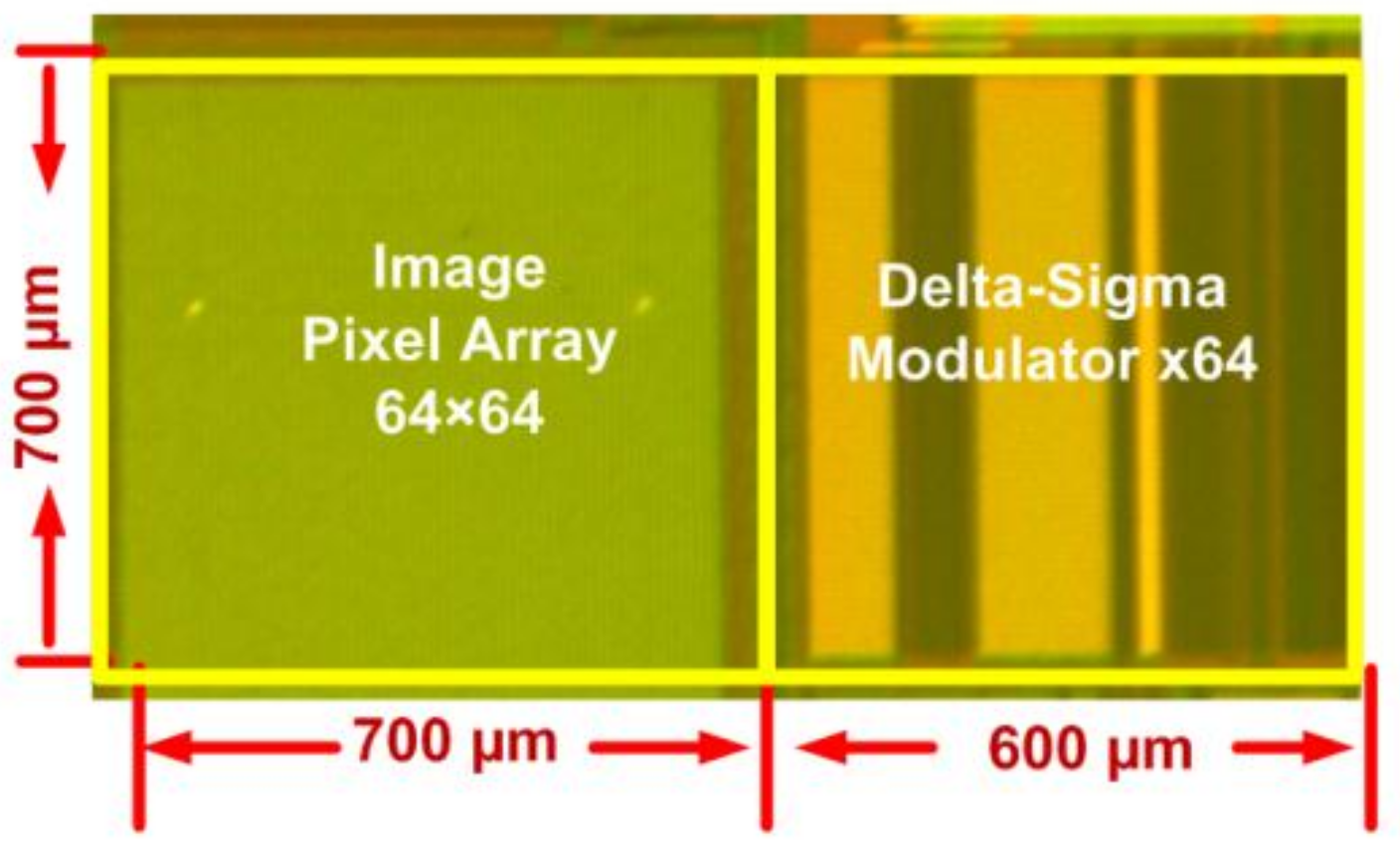
:1. Introduction
2. Pixel SF’s Temperature and Process Dependency, Process Sensor, and Temperature Sensor
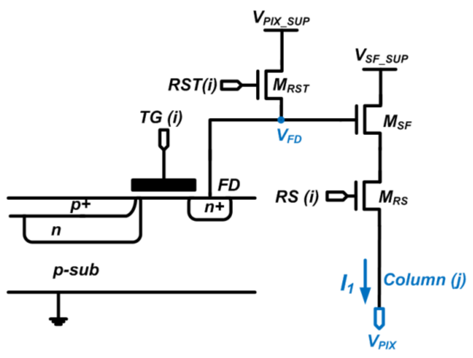
2.1. Pixel SF’s Temperature and Process Dependency
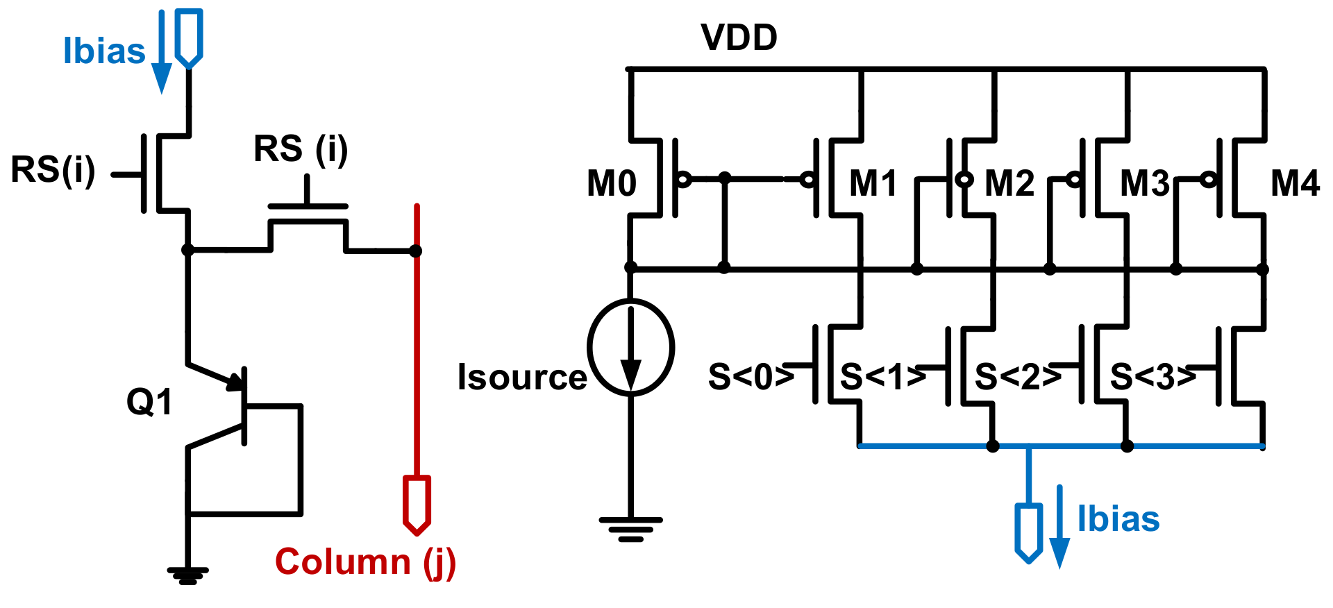
2.2. Process Sensors
2.3. Temperature Sensors
3. Measurement Results of SF’s Temperature and Process Dependency, Temperature, and Process Sensors
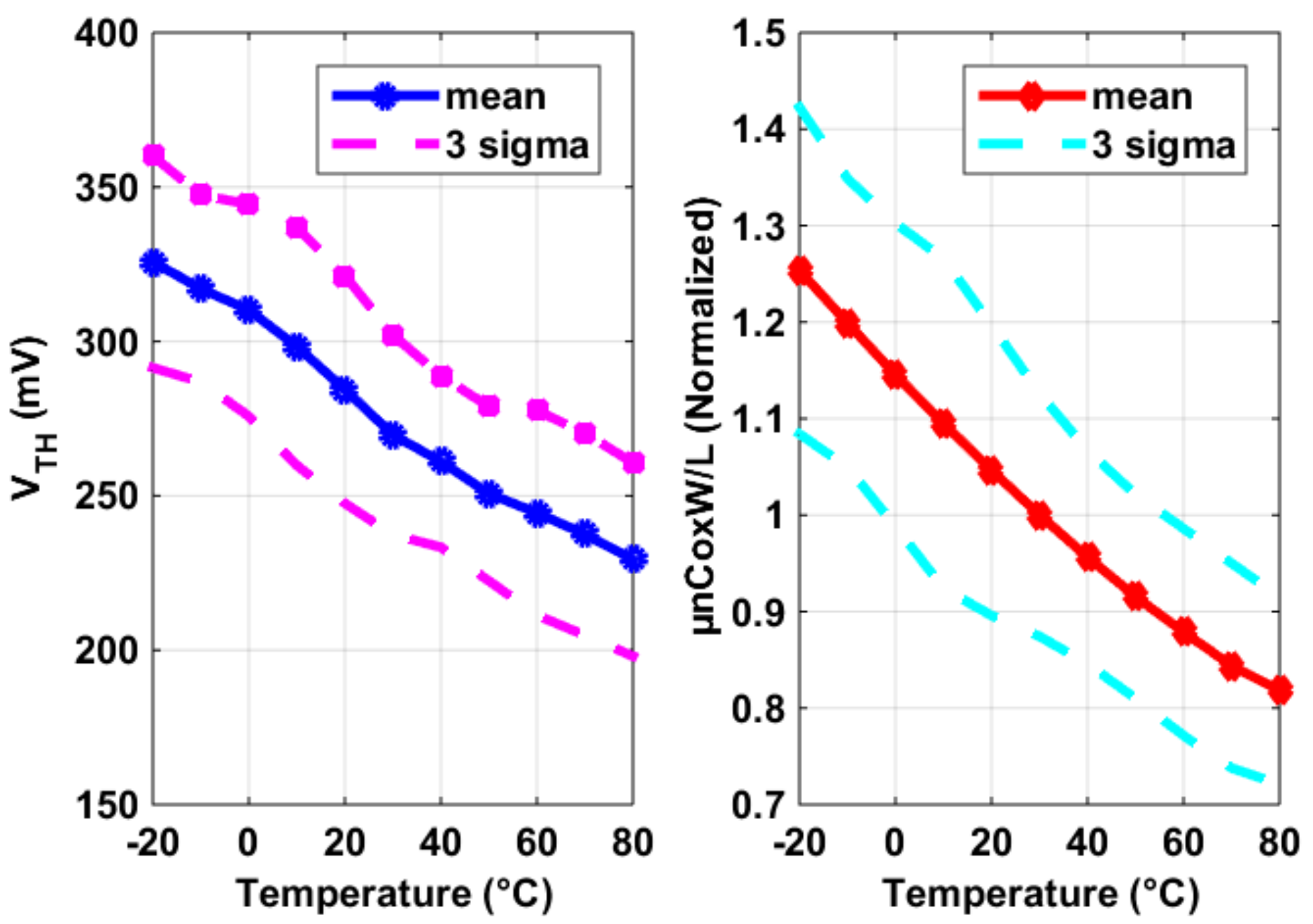
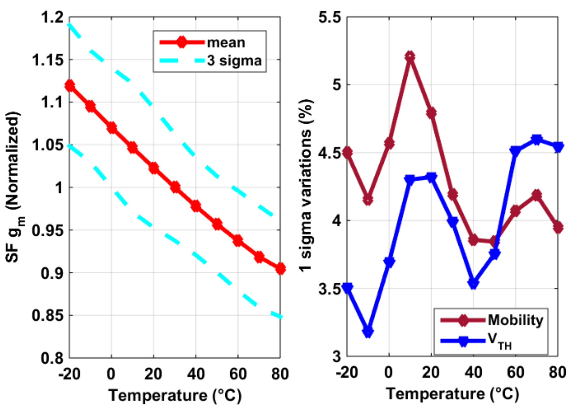
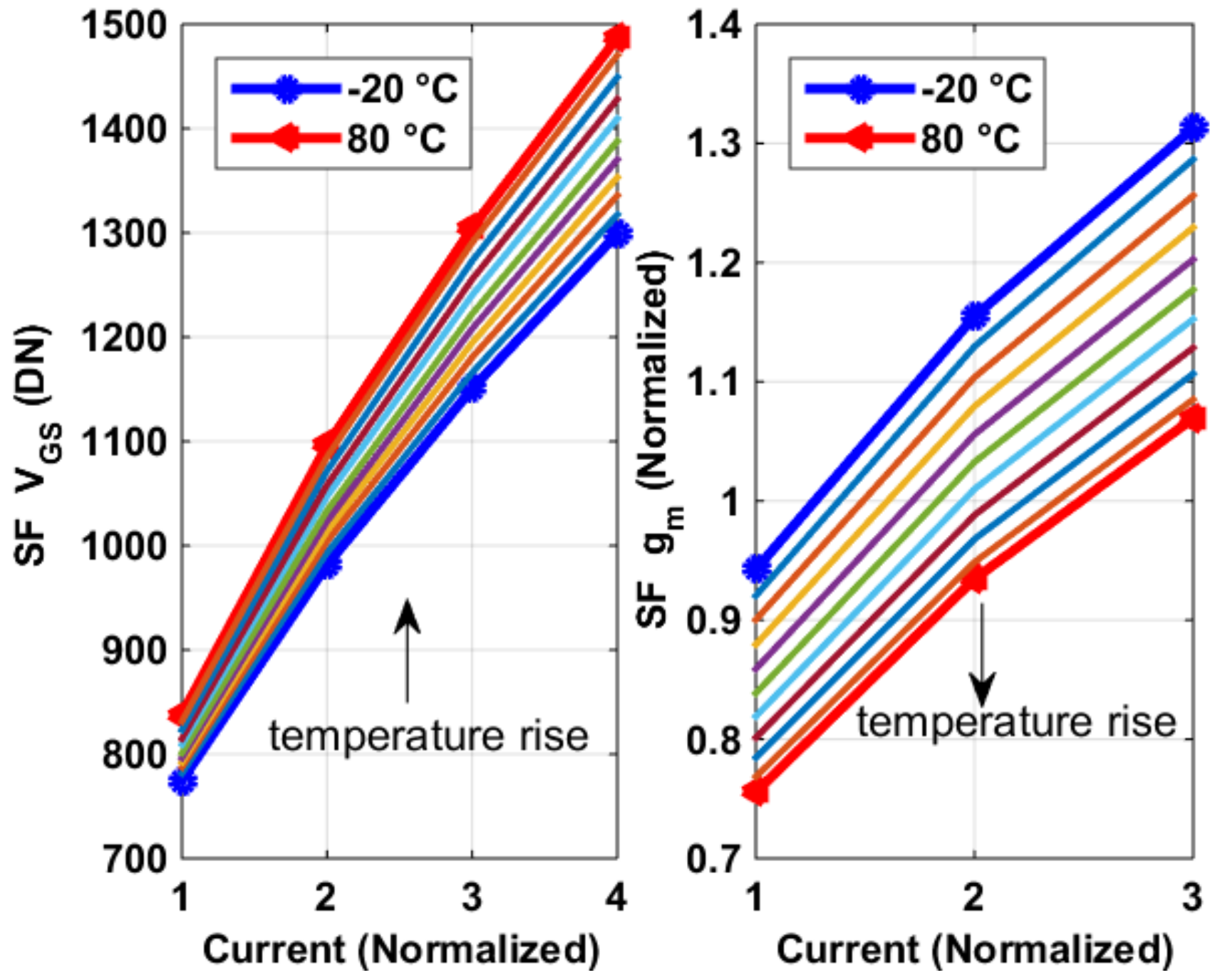
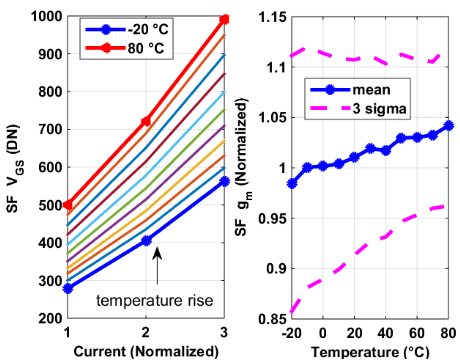
3.1. Pixel SF’s Temperature and Process Dependency
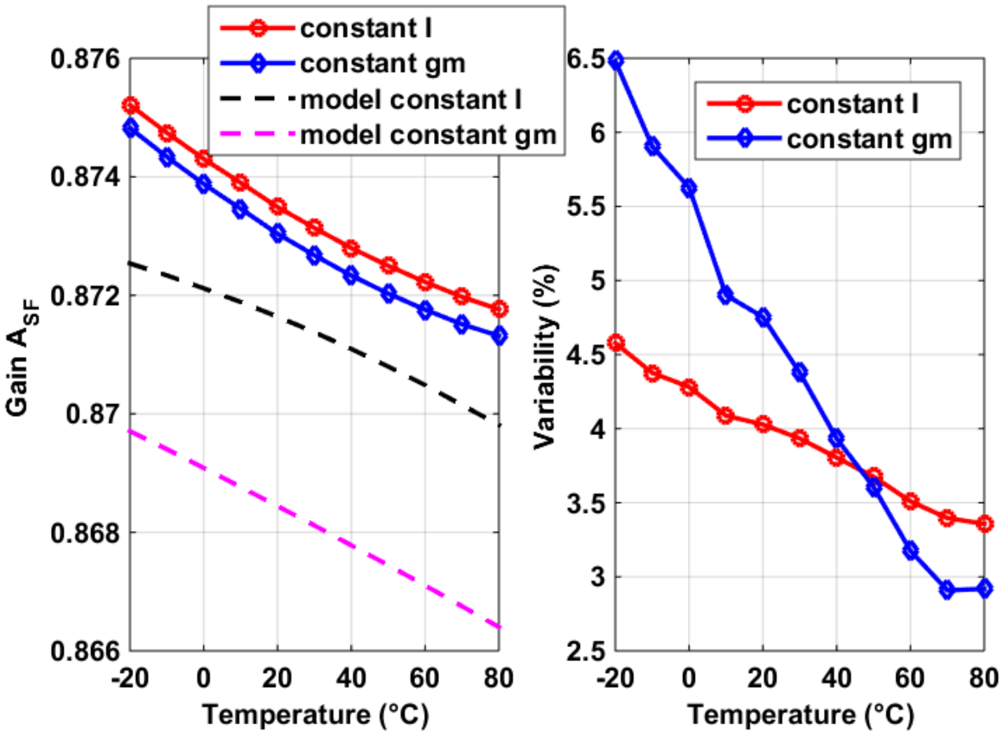
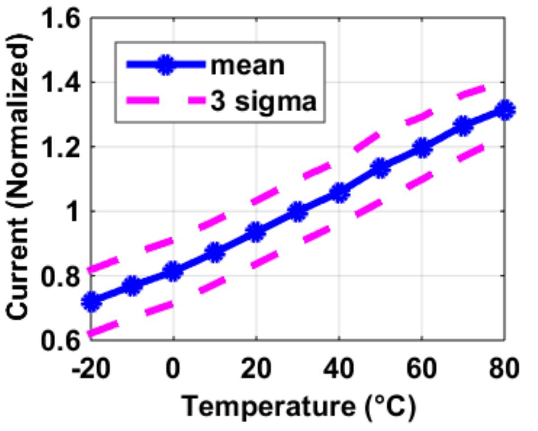
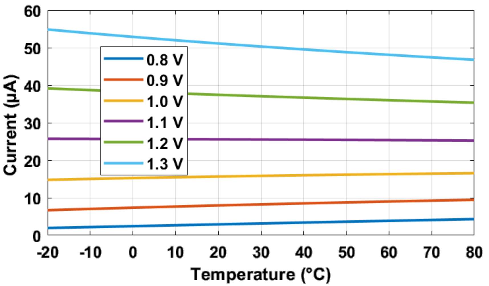
3.2. Process Sensor and SF Voltage Gain ASF
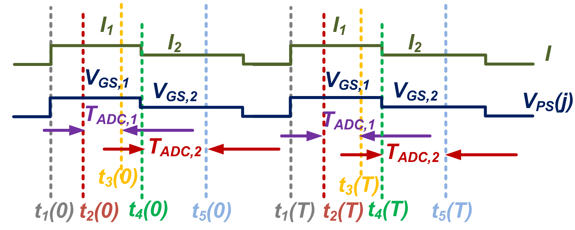
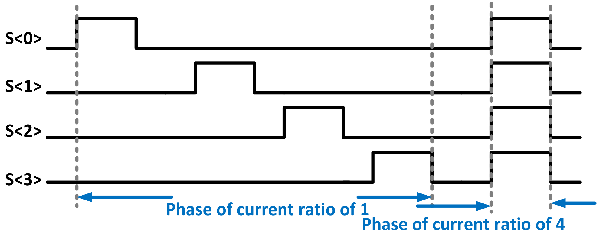
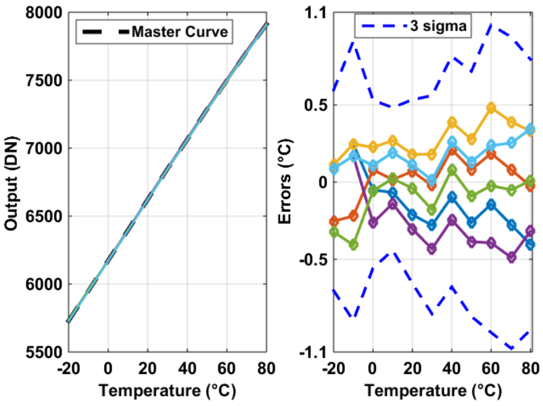
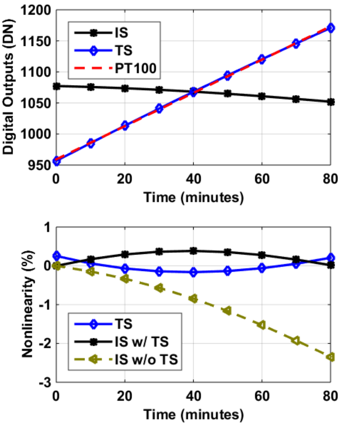
3.3. Measurement Results of BJT Based Temperature Sensors
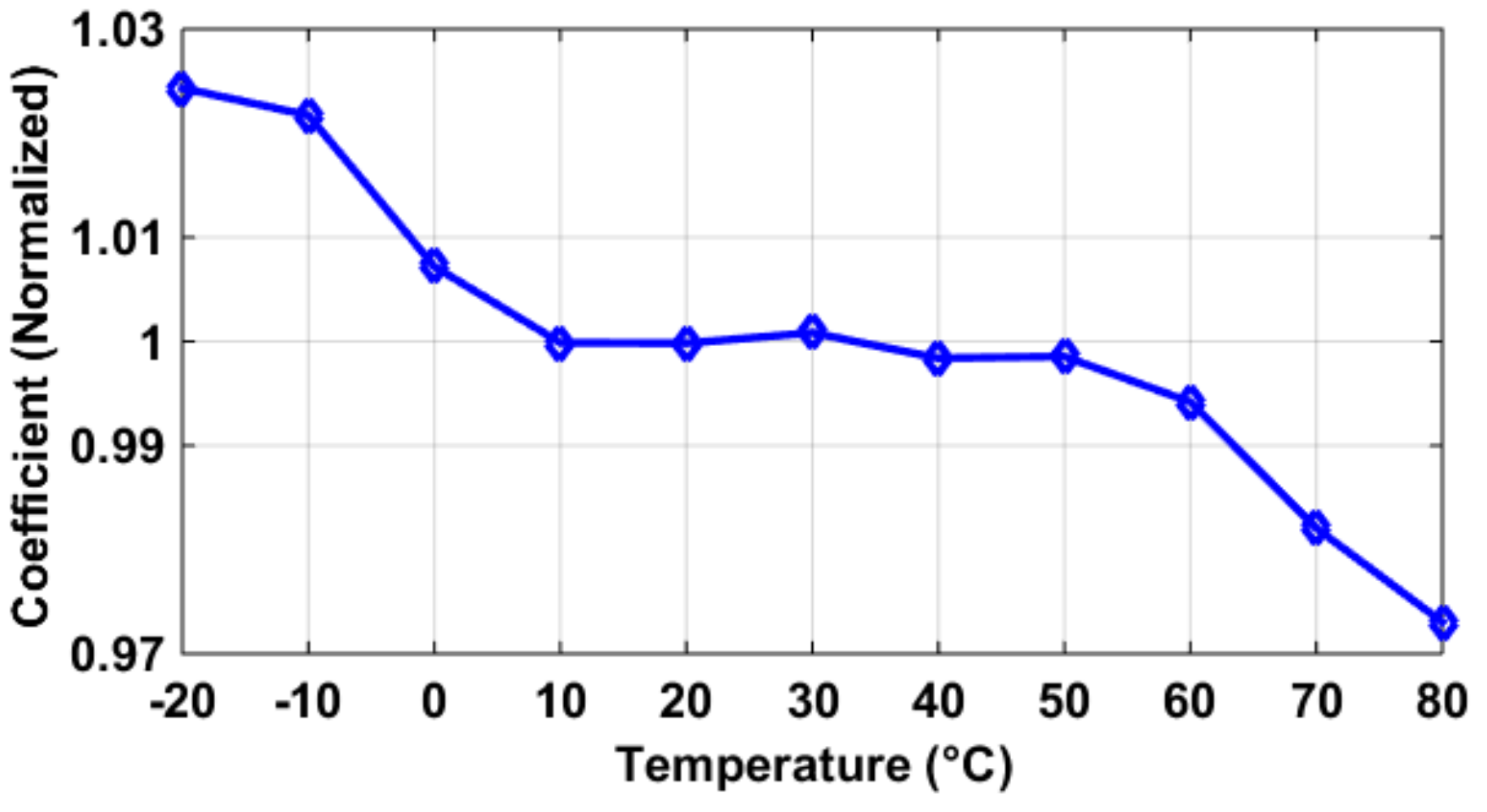
3.4. PGA/CDS and Constant Voltage Bias
4. Measurements and Compensation of Process and Temperature Dependency in a CIS
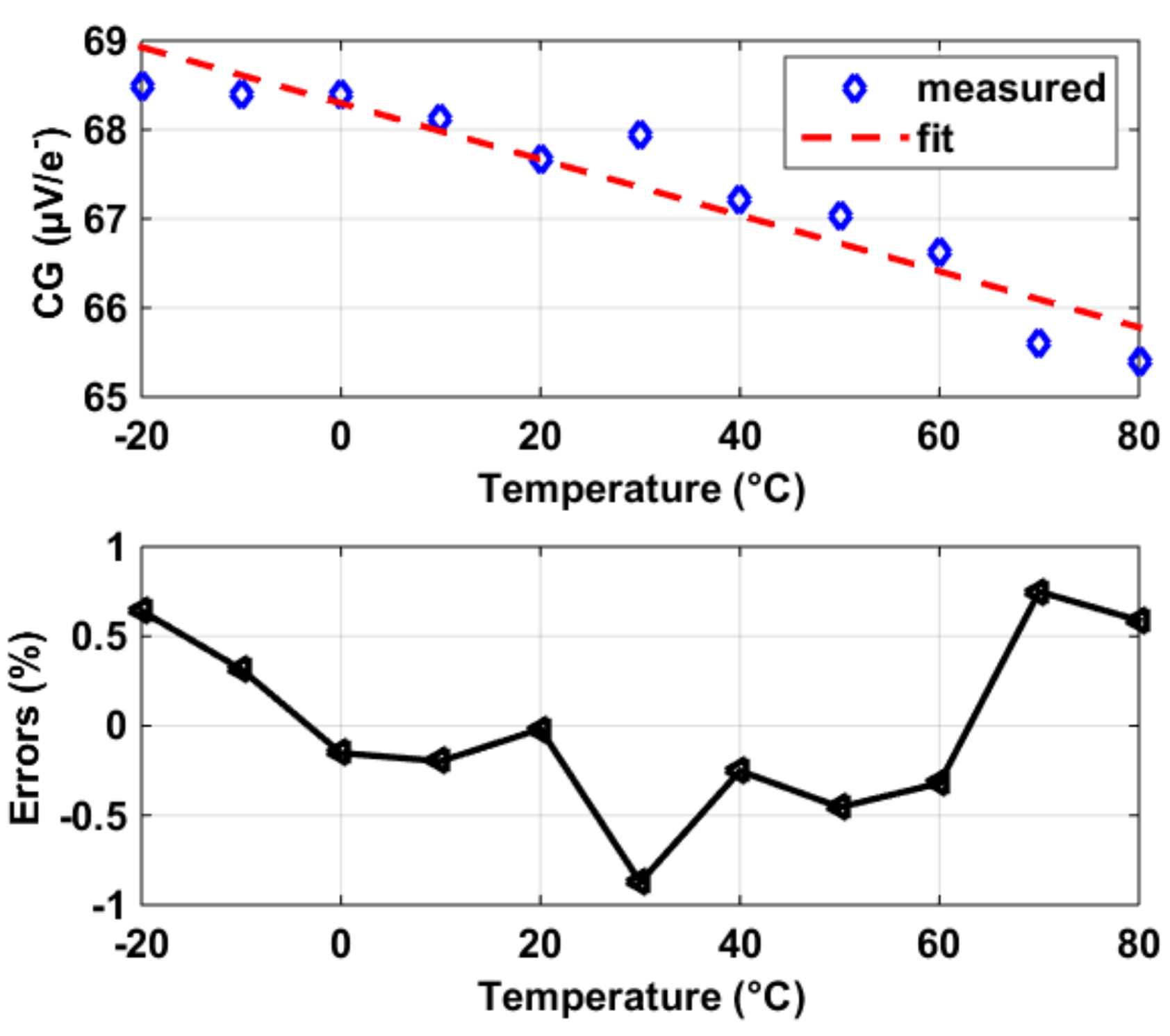
4.1. Conversion Gain (CG)
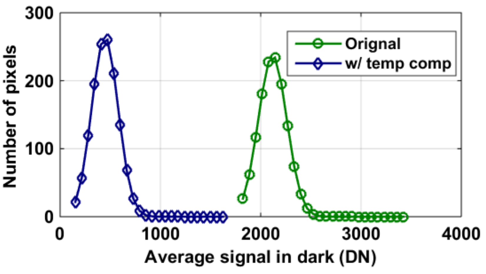
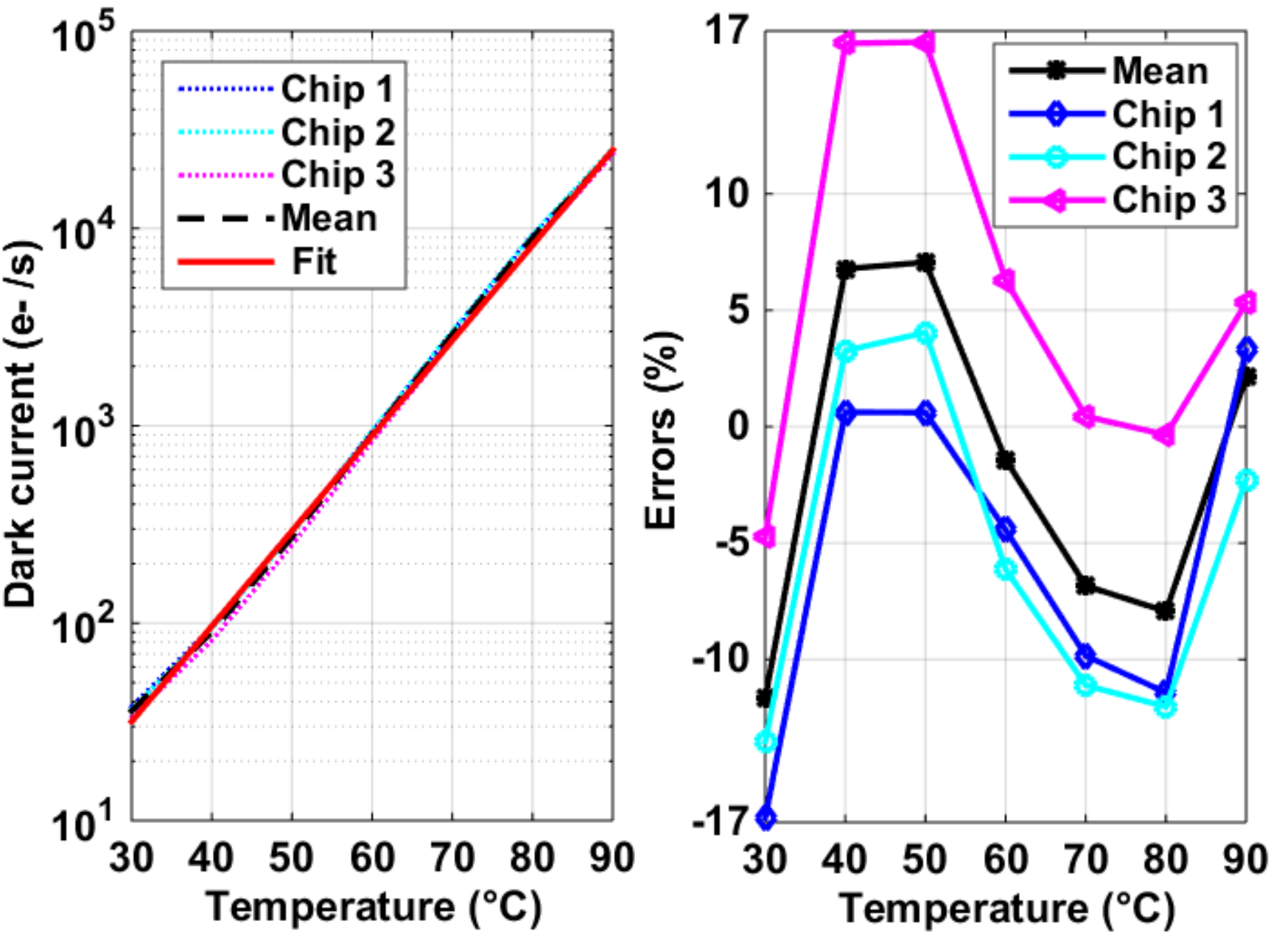
4.2. Dark Current and DSNU
5. Conclusions
Author Contributions
Funding
Acknowledgments
Conflicts of Interest
References
- Wang, X. Noise in Sub-Micron CMOS Image Sensors. Ph.D. Thesis, TU Delft, Delft, The Netherlands, 2008; pp. 46–68. [Google Scholar]
- Margarit, J.M.; Vergara, G.; Villamayor, V.; Gutiérrez-Álvarez, R.; Fernández-Montojo, C.; Terés, L.; Serra-Graells, F. A 2 kfps sub-µW/pix uncooled-PbSe digital imager with 10 bit DR adjustment and FPN correction for high-speed and low-cost MWIR applications. IEEE J. Solid-State Circuits 2015, 50, 2394–2405. [Google Scholar] [CrossRef]
- Xie, S.; Abarca, A.; Markenhof, J.; Ge, X.; Theuwissen, A. Analysis and calibration of process variations for an array of temperature sensors. In Proceedings of 2017 IEEE SENSORS, Glasgow, Scotland, UK, 29 October–1 November 2017; pp. 1–3. [Google Scholar]
- Abarca, A.; Xie, S.; Markenhof, J.; Theuwissen, A. Integration of 555 temperature sensors into a 64 × 192 CMOS image sensor. Sens. Actuators A Phys. 2018, 282, 243–250. [Google Scholar] [CrossRef]
- Wang, F.; Theuwissen, A.J.P. Temperature effect on the linearity performance of a CMOS image sensor. IEEE Sens. Lett. 2018, 2, 1–4. [Google Scholar] [CrossRef]
- Sarkar, M.; Büttgen, B.; Theuwissen, A.J.P. Temperature effects on feedforward voltage in standard CMOS pinned photodiodes. IEEE Trans. Electron Devices 2016, 63, 1963–1968. [Google Scholar] [CrossRef]
- Wang, F.; Han, L.; Theuwissen, A.J.P. Development and evaluation of a highly linear CMOS image sensor with a digitally assisted linearity calibration. IEEE J. Solid-State Circuits 2018, 53, 2970–2981. [Google Scholar] [CrossRef]
- Ha, D.; Woo, K.; Meninger, S.; Xanthopoulos, T.; Crain, E.; Ham, D. Time-domain CMOS temperature sensors with dual delay-locked loops for microprocessor thermal monitoring. IEEE Trans. Very Large Scale Integr. Syst. 2012, 20, 1590–1601. [Google Scholar] [CrossRef]
- Pertijs, M.A.P.; Huijsing, J.H. Precision Temperature Sensors in CMOS Technology; Springer: Dordrecht, The Netherlands, 2006; pp. 213–225. [Google Scholar]
- Vosooghi, B.; Lu, L. 5 × 5 scattered temperature sensor front-end based on single-diode with non-trimmed ±0.7 °C 3σ relative inaccuracy. Electron. Lett. 2014, 50, 1806–1808. [Google Scholar] [CrossRef]
- Yokoyama, T.; Tsutsui, M.; Suzuki, M.; Nishi, Y.; Mizuno, I.; Lahav, A. Development of low parasitic light sensitivity and low dark current 2.8 μm global shutter pixel. Sensors 2018, 18, 349. [Google Scholar] [CrossRef] [PubMed]
- Carusone, T.C.; Johns, D.A.; Martin, K.W. Analog Integrated Circuit Design; Wiley: Hoboken, NJ, USA, 2012; pp. 100–101. [Google Scholar]
- Zhang, M.; Noh, K.; Fan, X.; Sánchez-Sinencio, E. A temperature compensation technique for a dynamic amplifier in pipelined-SAR ADCs. IEEE Solid-State Circuits Lett. 2018, 1, 10–13. [Google Scholar] [CrossRef]
- Xie, S.; Ng, W.T. A 0.02 nJ self-calibrated 65 nm CMOS delay line temperature sensor. In In Proceedings of the 2012 IEEE International Symposium on Circuits and Systems (ISCAS), Seoul, Korea, 19–23 May 2012; pp. 3126–3129. [Google Scholar]
- Tang, Z.; Tan, N.N.; Shi, Z.; Yu, X. A 1.2V self-referenced temperature sensor with a time-domain readout and a two-step improvement on output dynamic range. IEEE Sens. J. 2018, 18, 1849–1858. [Google Scholar] [CrossRef]
- Cochet, M.; Keller, B.; Clerc, S.; Abouzeid, F.; Cathelin, A.; Autran, J.; Roche, P.; Nikolić, B. A 225 μm2 probe single-point calibration digital temperature sensor using body-bias adjustment in 28 nm FD-SOI CMOS. IEEE Solid-State Circuits Lett. 2018, 1, 14–17. [Google Scholar] [CrossRef]
- Makinwa, K. Smart Temperature Sensor Survey. Available online: https://ei.tudelft.nl/smart_temperature/ (accessed on 10 September 2018).


| This Work | [15] | [16] | |
|---|---|---|---|
| Sensor Type | BJT | BJT | MOS |
| CMOS Technology | 0.18 µm | 0.13 µm | 28 nm |
| Area (µm2) | 121 | 60,000 | 1000 |
| Temperature Range | −20 °C to 80 °C | −20 °C to 100 °C | −5 °C to 85 °C |
| 3 σ accuracy | ±1.1 °C | −1.7/1.26 °C | −3.3/1.9 °C |
| Calibration | Un-trimmed | Two-point | One-point |
| Power Consumption (µW) | 36 | 744 | 56 |
| Conversion Time (ms) | 16 | 13.3 | 0.036 |
| Resolution (°C) | 0.09 | 0.187 | 0.76 |
| Resolution FOM (nJ∙K2)a | 4.6 | 346 | 1.2 |
| Rel.IA (%)b | 2.2 | 2.4 | 5.8 |
© 2019 by the authors. Licensee MDPI, Basel, Switzerland. This article is an open access article distributed under the terms and conditions of the Creative Commons Attribution (CC BY) license (http://creativecommons.org/licenses/by/4.0/).
Share and Cite
Xie, S.; Theuwissen, A. Compensation for Process and Temperature Dependency in a CMOS Image Sensor. Sensors 2019, 19, 870. https://doi.org/10.3390/s19040870
Xie S, Theuwissen A. Compensation for Process and Temperature Dependency in a CMOS Image Sensor. Sensors. 2019; 19(4):870. https://doi.org/10.3390/s19040870
Chicago/Turabian StyleXie, Shuang, and Albert Theuwissen. 2019. "Compensation for Process and Temperature Dependency in a CMOS Image Sensor" Sensors 19, no. 4: 870. https://doi.org/10.3390/s19040870
APA StyleXie, S., & Theuwissen, A. (2019). Compensation for Process and Temperature Dependency in a CMOS Image Sensor. Sensors, 19(4), 870. https://doi.org/10.3390/s19040870