High Sensitivity Flexible Electronic Skin Based on Graphene Film


Abstract
1. Introduction
2. Materials and Methods
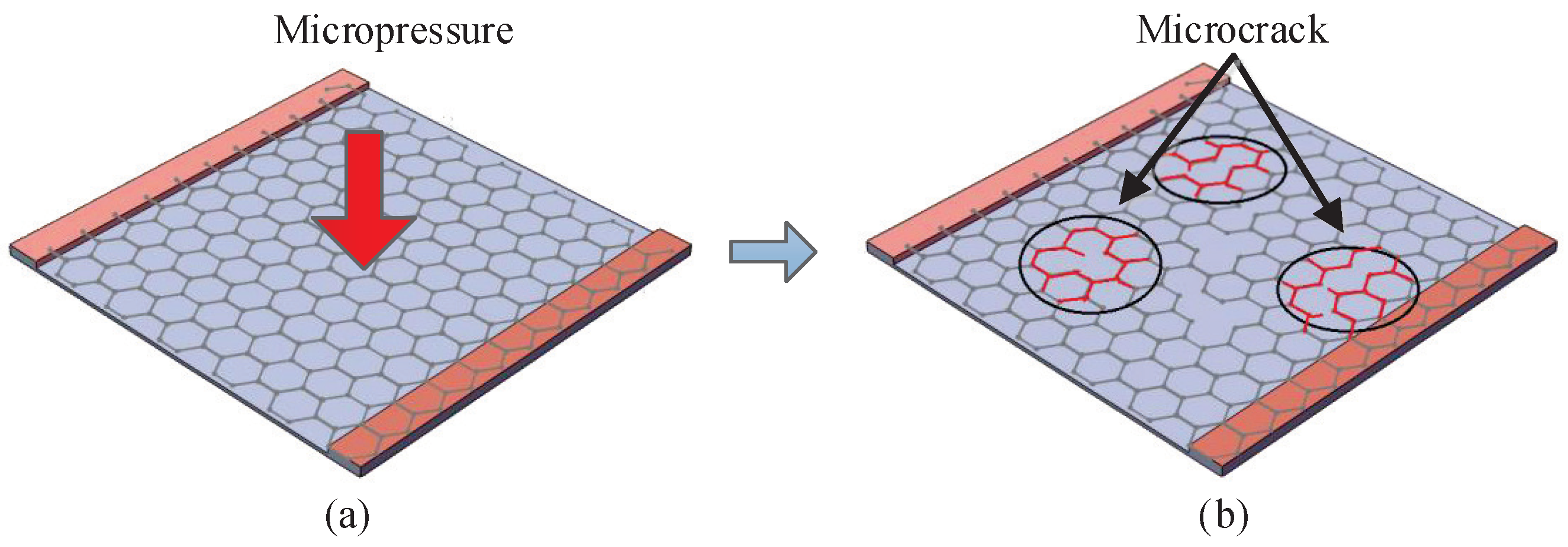
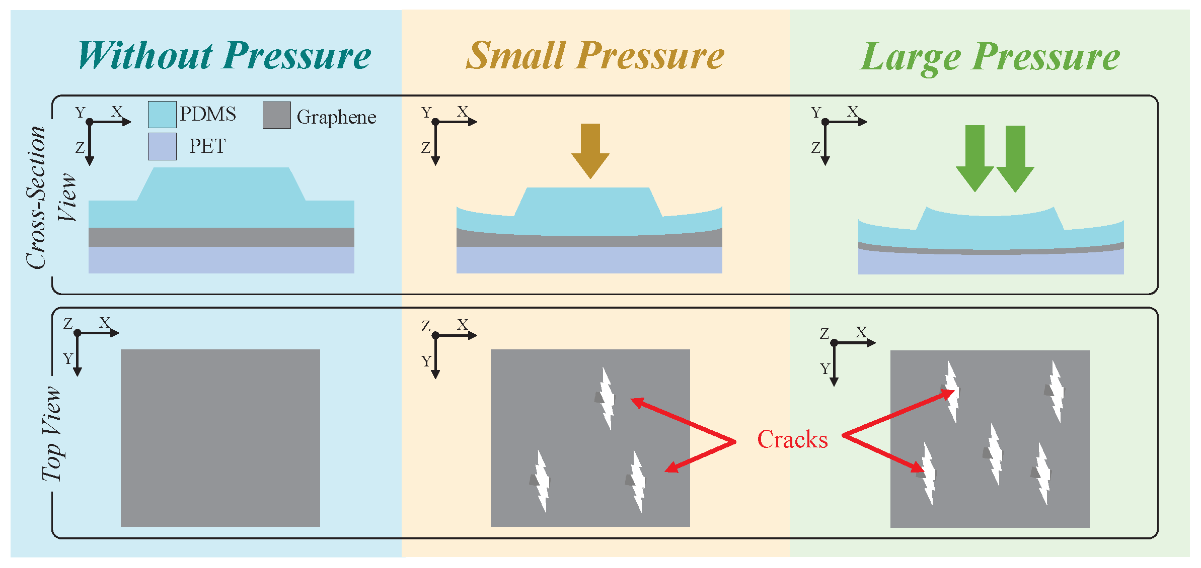
2.1. Principle
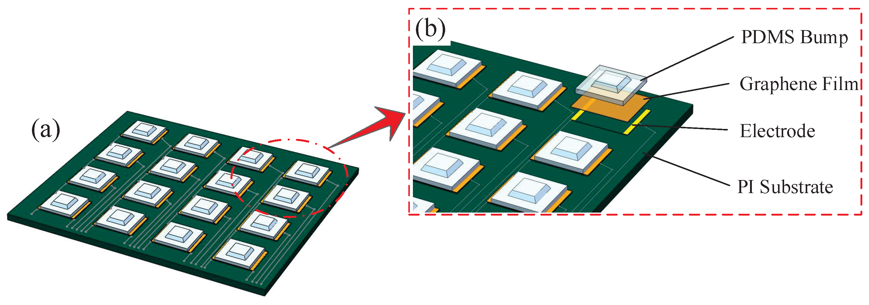
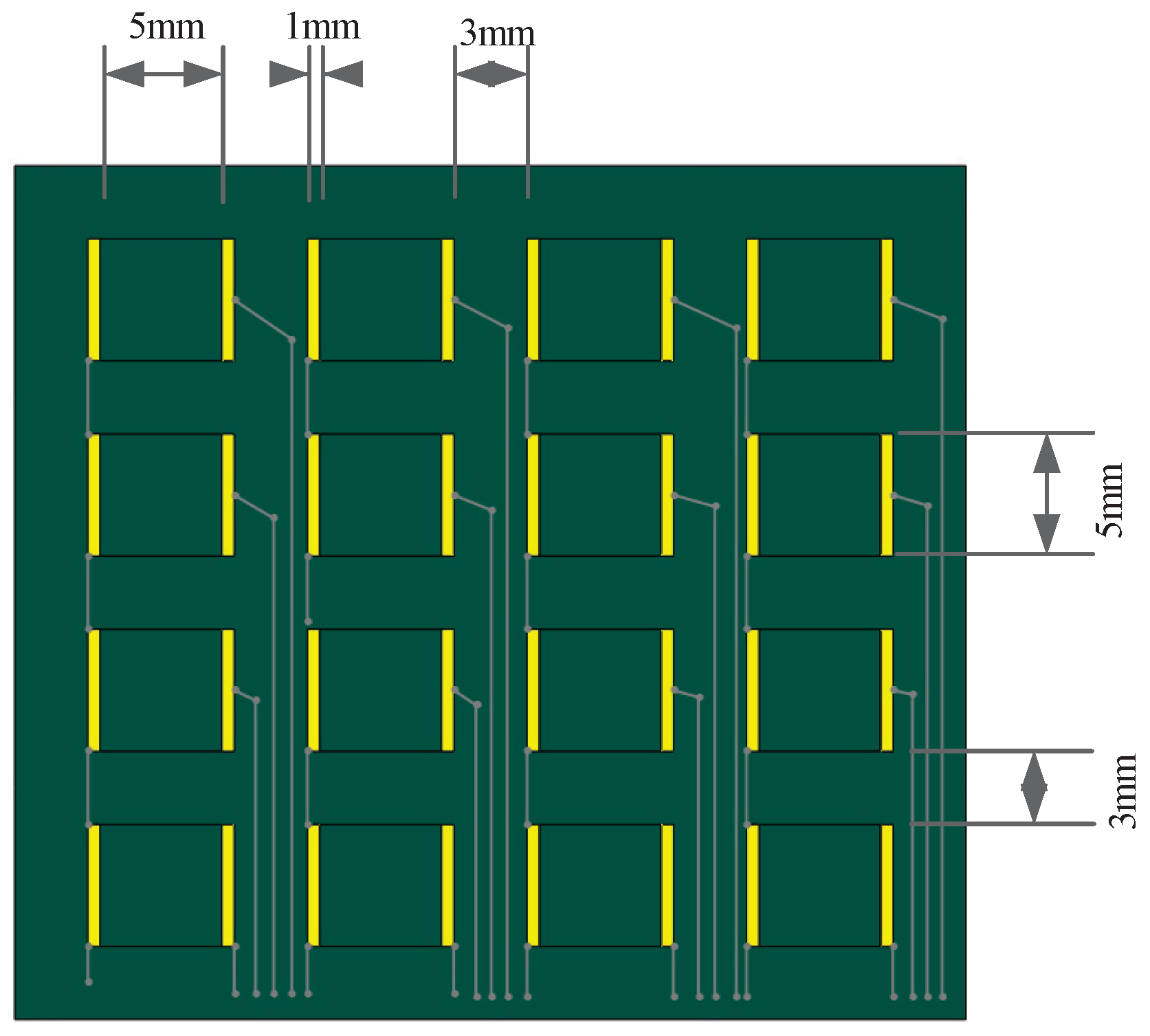
2.2. Structure
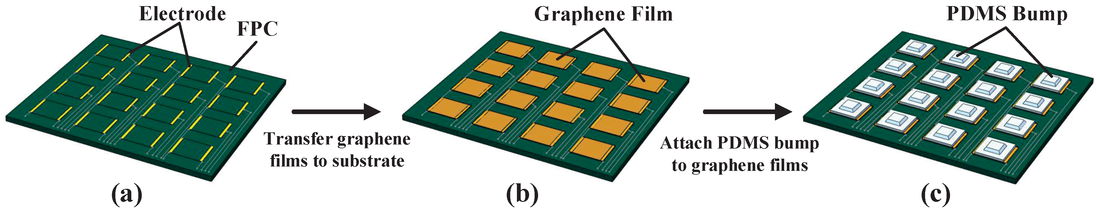
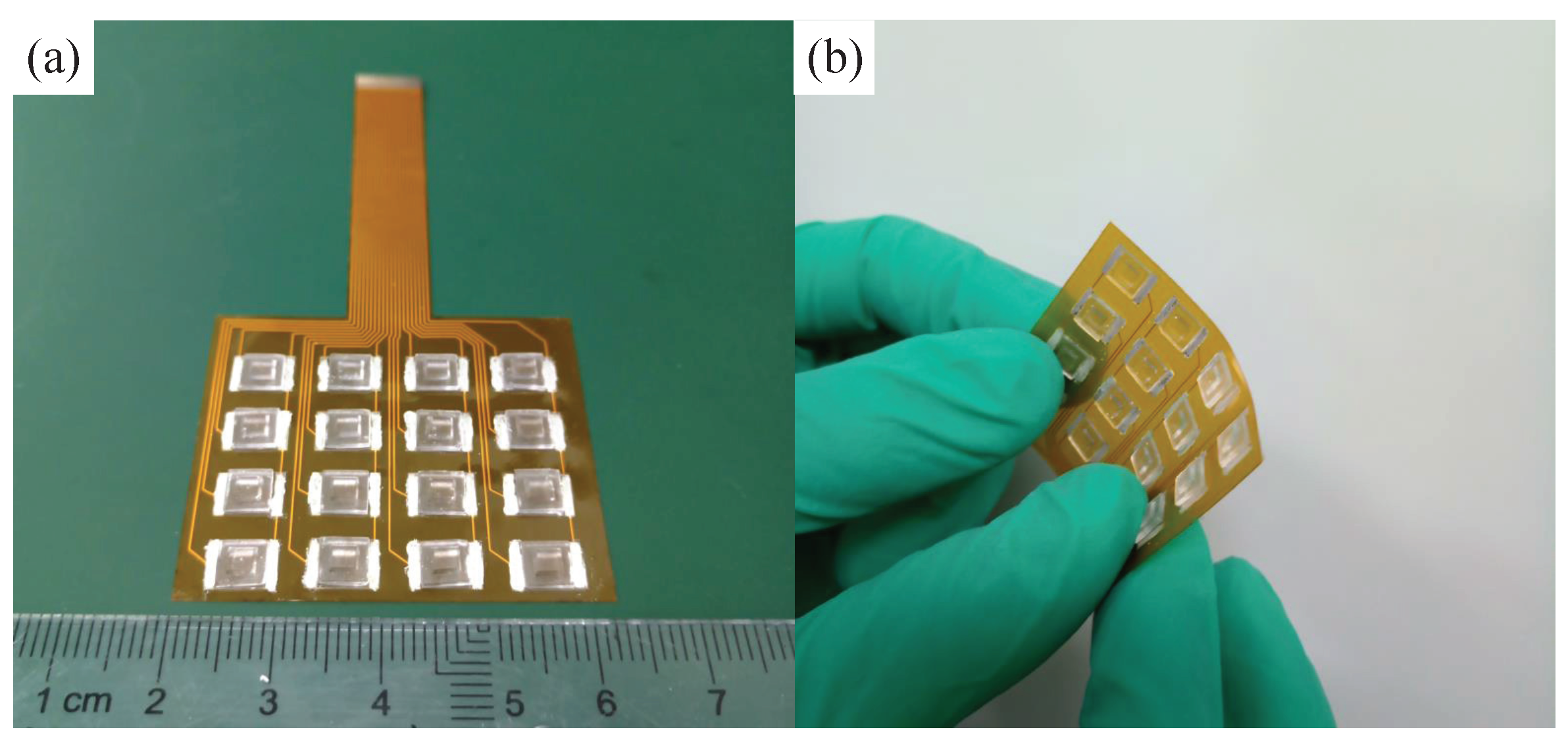
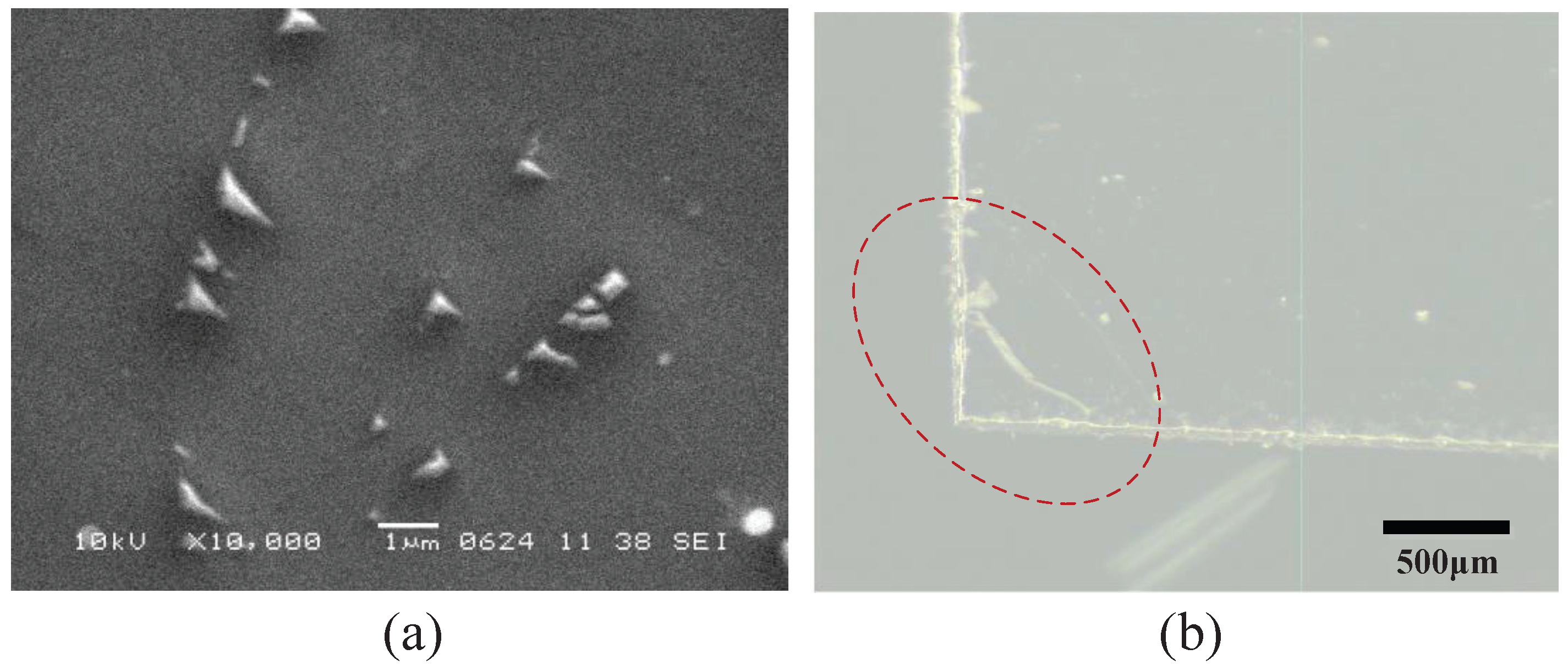
2.3. Fabrication Process
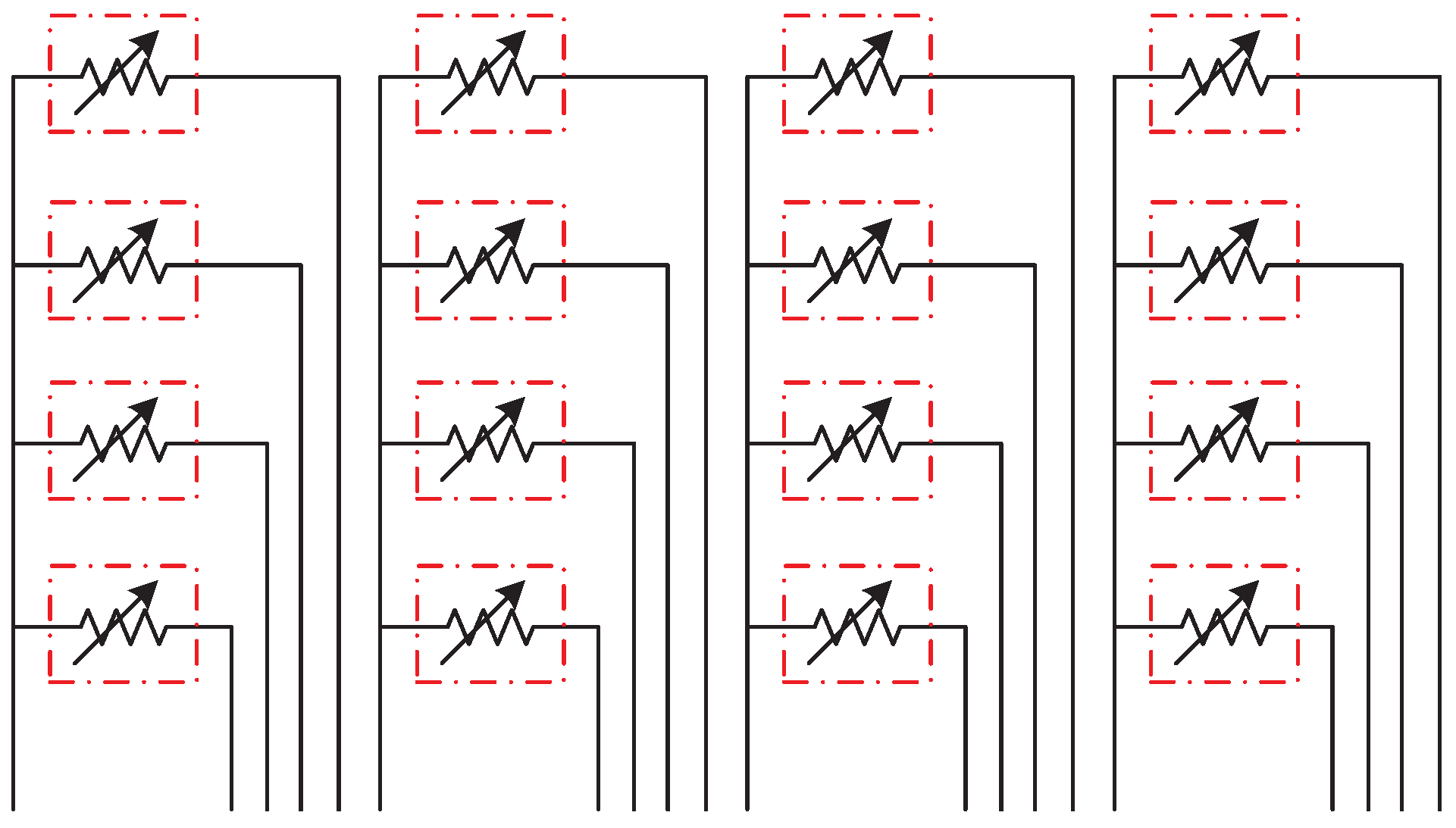
2.4. Circuit Model
2.5. Measurement Model
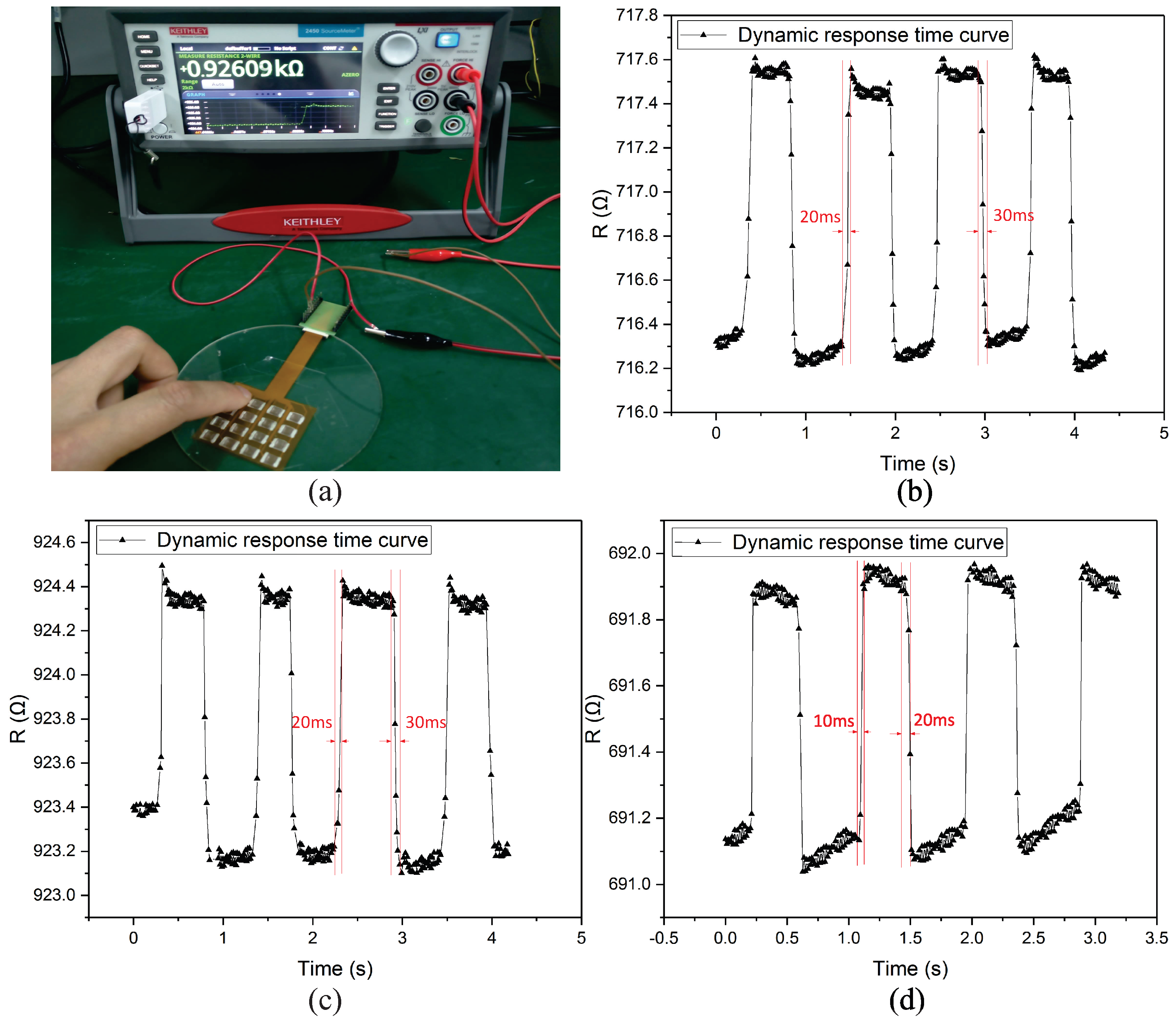
3. Experiment
4. Results and Discussion
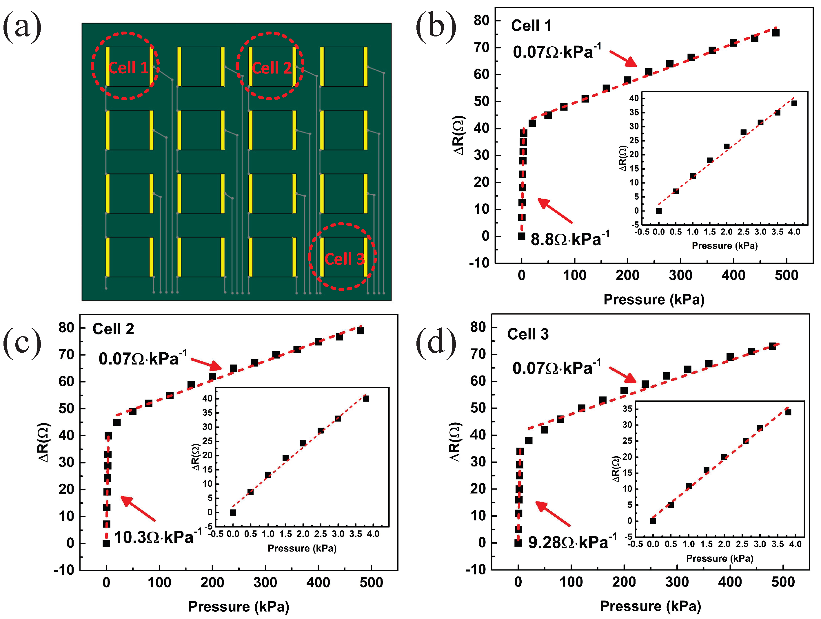
4.1. Measurement Model
4.2. Sensitivity
4.3. Dynamic Characteristic
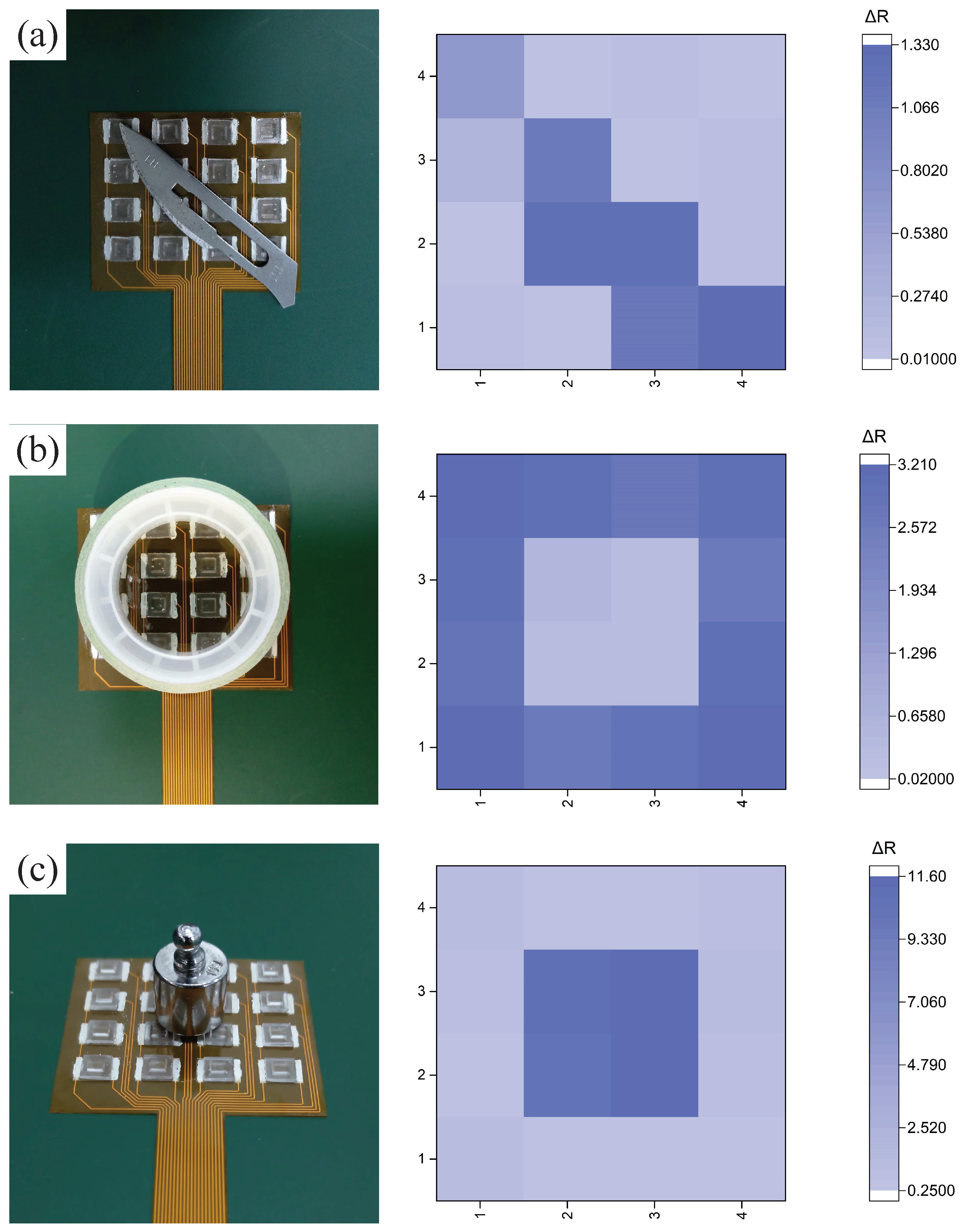
4.4. Consistency
4.5. Application
4.6. Comparison
5. Conclusions
Author Contributions
Funding
Conflicts of Interest
References
- Hammock, M.L.; Chortos, A.; Tee, B.C.K.; Tok, J.B.H.; Bao, Z.N. 25th Anniversary Article: The Evolution of Electronic Skin (E-Skin): A Brief History, Design Considerations, and Recent Progress. Adv. Mater. 2013, 25, 5997–6037. [Google Scholar] [CrossRef] [PubMed]
- Wang, X.W.; Liu, Z.; Zhang, T. AFlexible Sensing Electronics for Wearable/Attachable Health Monitoring. Small 2017, 13, 1602790. [Google Scholar] [CrossRef] [PubMed]
- Tan, Y.J.; Wu, J.K.; Li, H.Y.; Tee, B.C.K. Self-Healing Electronic Materials for a Smart and Sustainable Future. ACS Appl. Mater. Interfaces 2018, 10, 15331–15345. [Google Scholar] [CrossRef] [PubMed]
- Yang, J.Y.; Ye, Y.S.; Li, X.P.; Lü, X.Z.; Chen, R.J. Flexible, conductive, and highly pressure-sensitive graphene-polyimide foam for pressure sensor application. Compos. Sci. Technol. 2018, 164, 187–194. [Google Scholar] [CrossRef]
- Chi, C.; Sun, X.G.; Xue, N.; Li, T.; Liu, C. Recent Progress in Technologies for Tactile Sensors. Sensors 2018, 18, 948. [Google Scholar] [CrossRef] [PubMed]
- Lee, Y.; Park, J.; Cho, S.; Shin, Y.; Lee, H.; Kim, J.; Myoung, J.; Cho, S.; Kang, S.; Baig, C.; et al. Flexible Ferroelectric Sensors with Ultrahigh Pressure Sensitivity and Linear Response over Exceptionally Broad Pressure Range. ACS Nano 2018, 12, 689–798. [Google Scholar] [CrossRef] [PubMed]
- Jin, M.; Park, S.; Lee, Y.; Lee, J.; Chung, J.; Kim, J.; Kim, J.; Kim, S.; Jee, E.; Kim, D.; et al. An Ultrasensitive, Visco-Poroelastic Artificial Mechanotransducer Skin Inspired by Piezo2 Protein in Mammalian Merkel Cells. Adv. Mater. 2017, 29, 1605973. [Google Scholar] [CrossRef] [PubMed]
- Kang, S.; Lee, J.; Lee, S.; Kim, S.; Kim, J.; Algadi, H.; Sayari, S.; Kim, D.; Kim, D.; Lee, T. Highly Sensitive Pressure Sensor Based on Bioinspired Porous Structure for Real-Time Tactile Sensing. Adv. Electron. Mater. 2016, 2, 1600356. [Google Scholar] [CrossRef]
- Ha, M.J.; Lim, S.D.; Ko, H.H. Wearable and flexible sensors for user-interactive health-monitoring devices. J. Mater. Chem. B 2018, 6, 4043–4064. [Google Scholar] [CrossRef]
- Zang, Y.P.; Zhang, F.J.; Di, C.A.; Zhu, D.B. Advances of flexible pressure sensors toward artificial intelligence and health care applications. Mater. Horiz. 2015, 2, 140–156. [Google Scholar] [CrossRef]
- Yang, J.Y.; Li, X.P.; Lü, X.Z.; Chen, W.M.B.R.J. Three-Dimensional Interfacial Stress Sensor Based on Graphene Foam. IEEE Sens. J. 2018, 18, 7956–7963. [Google Scholar] [CrossRef]
- Lü, X.Z.; Bao, W.M.; Tao, Y.B.; Yang, J.Y.; Jiang, L.; Jiang, J.N.; Li, X.P.; Xie, K.; Chen, R.J. Three-Dimensional Interfacial Stress Decoupling Method for Rehabilitation Therapy Robot. IEEE Trans. Ind. Electron. 2017, 64, 3970–3977. [Google Scholar] [CrossRef]
- Gao, W.; Emaminejad, S.; Nyein, H.Y.Y.; Challa, S.; Chen, K.; Peck, A.; Fahad, H.M.; Ota, H.; Shiraki, H.; Kiriya, D.; et al. Fully integrated wearable sensor arrays for multiplexed in situ perspiration analysis. Nature 2016, 529, 509–514. [Google Scholar] [CrossRef] [PubMed]
- Minev, I.R.; Musienko, P.; Hirsch, A.; Barraud, Q.; Wenger, N.; Moraud, E.M.; Gandar, J.; Capogrosso, M.; Milekovic, T.; Asboth, L.; et al. Electronic dura mater for long-term multimodal neural interfaces. Science 2015, 347, 159–163. [Google Scholar] [CrossRef] [PubMed]
- Chortos, A.; Liu, J.; Bao, Z.N. Pursuing prosthetic electronic skin. Nat. Mater. 2016, 15, 937–950. [Google Scholar] [CrossRef]
- Tawil, D.S.; Rye, D.; Velonaki, M. Artificial skin and tactile sensing for socially interactive robots: A review. Robot. Auton. Syst. 2015, 63, 230–243. [Google Scholar] [CrossRef]
- Joo, Y.S.; Yoon, J.Y.; Ha, J.W.; Kim, T.H.; Lee, S.W.; Lee, B.M.; Pang, C.Y.; Hong, Y.T. Highly Sensitive and Bendable Capacitive Pressure Sensor and Its Application to 1 V Operation Pressure-Sensitive Transistor. Adv. Electron. Mater. 2017, 3, 1600455. [Google Scholar] [CrossRef]
- Lipomi, D.J.; Cosgueritchian, M.; Tee, B.C.K.; Hellstrom, S.L.; Lee, J.A.; Fox, C.H.; Bao, Z.N. Skin-like pressure and strain sensors based on transparent elastic films of carbon nanotubes. Nat. Nanotechnol. 2011, 6, 788–792. [Google Scholar] [CrossRef]
- Yu, G.H.; Hu, J.D.; Tan, J.P.; Gao, Y.; Lu, Y.F.; Xuan, F.Z. A wearable pressure sensor based on ultra-violet/ozone microstructured carbon nanotube/polydimethylsiloxane arrays for electronic skins. Nanotechnology 2018, 29, 115502. [Google Scholar] [CrossRef]
- Gong, S.; Schwalb, W.; Wang, Y.W.; Chen, Y.; Tang, Y.; Si, J.; Shirinzadeh, B.J.; Cheng, W.L. A wearable and highly sensitive pressure sensor with ultrathin gold nanowires. Nat. Commun. 2014, 5, 3132. [Google Scholar] [CrossRef]
- Sun, Q.J.; Kim, D.H.; Park, S.S.; Lee, N.Y.; Zhang, Y.; Lee, J.H.; Cho, K.; Cho, J.H. Transparent, Low-Power Pressure Sensor Matrix Based on Coplanar-Gate Graphene Transistors. Adv. Mater. 2014, 26, 4735–4740. [Google Scholar] [CrossRef] [PubMed]
- Pang, Y.; Tian, H.; Tao, L. Flexible, Highly Sensitive, and Wearable Pressure and Strain Sensors with Graphene Porous Network Structure. ACS Appl. Mater. Interfaces 2016, 8, 26458–26462. [Google Scholar] [CrossRef] [PubMed]
- Jung, J.D.; Lee, D.G.; Park, J.W.; Ko, H.Y.; Lim, H. Piezoresistive Tactile Sensor Discriminating Multidirectional Forces. Sensors 2015, 15, 25463–25473. [Google Scholar] [CrossRef] [PubMed]


| Reference | Principle | Material | Sensitivity (kPa) | Measurement Range (kPa) | Response Times (ms) | Spatial Resolution |
|---|---|---|---|---|---|---|
| This Work | Piezoresistive | G/PET | 0.04 | 0 kPa–500 kPa | 20 | 5 mm |
| [21] | Transisitor | G/PET | 0.12 | 0 kPa–40 kPa | <10 | 2.5 mm |
| [18] | Capacitor | CNT | 0.004 | 0 kPa–50 kPa | 125 | 4 mm |
| [22] | Piezoresistive | AuNWs | 1.14 | 0 kPa–50 kPa | 17 | 5 mm |
| [23] | Capacitor | CNT/PDMS | 0.198 | 0 kPa–10 kPa | 200 | 8 mm |
© 2019 by the authors. Licensee MDPI, Basel, Switzerland. This article is an open access article distributed under the terms and conditions of the Creative Commons Attribution (CC BY) license (http://creativecommons.org/licenses/by/4.0/).
Share and Cite
Lü, X.; Yang, J.; Qi, L.; Bao, W.; Zhao, L.; Chen, R. High Sensitivity Flexible Electronic Skin Based on Graphene Film. Sensors 2019, 19, 794. https://doi.org/10.3390/s19040794
Lü X, Yang J, Qi L, Bao W, Zhao L, Chen R. High Sensitivity Flexible Electronic Skin Based on Graphene Film. Sensors. 2019; 19(4):794. https://doi.org/10.3390/s19040794
Chicago/Turabian StyleLü, Xiaozhou, Jiayi Yang, Liang Qi, Weimin Bao, Liang Zhao, and Renjie Chen. 2019. "High Sensitivity Flexible Electronic Skin Based on Graphene Film" Sensors 19, no. 4: 794. https://doi.org/10.3390/s19040794
APA StyleLü, X., Yang, J., Qi, L., Bao, W., Zhao, L., & Chen, R. (2019). High Sensitivity Flexible Electronic Skin Based on Graphene Film. Sensors, 19(4), 794. https://doi.org/10.3390/s19040794