A CMOS Low Pass Filter for SoC Lock-in-Based Measurement Devices


Abstract
1. Introduction
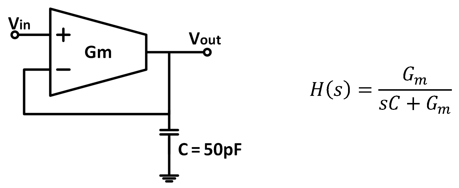
2. Proposed Gm-C LPF
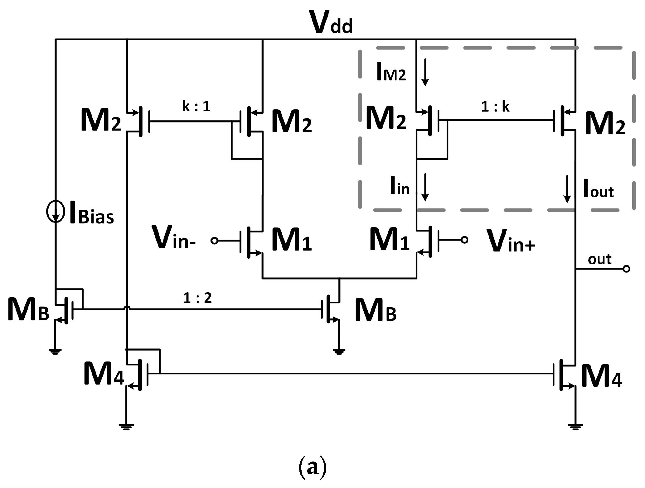
2.1. Transconductor Architecture
2.2. O1-Filter: O1F
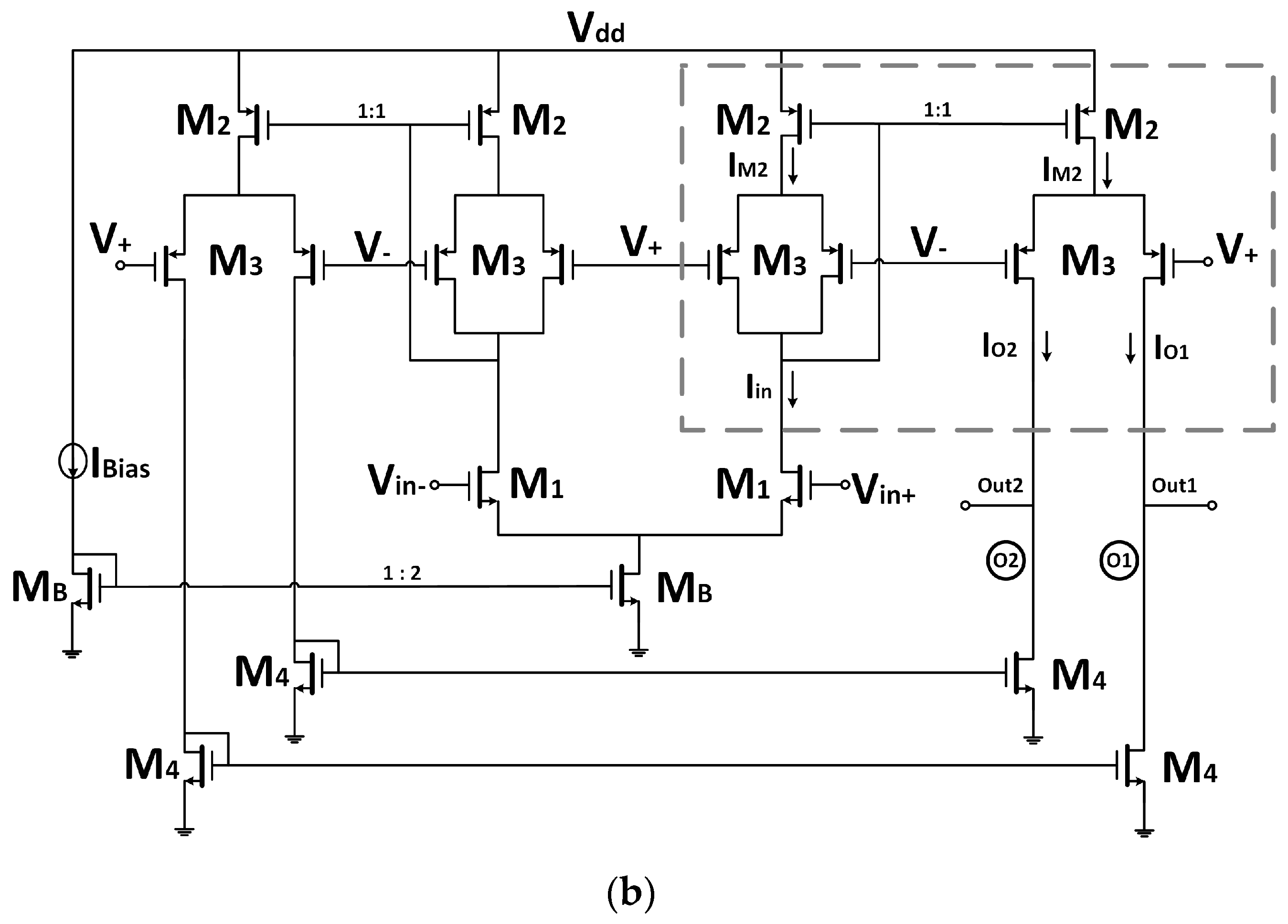
2.3. O2-Filter: O2F
3. Experimental Results
3.1. Experimental Setup
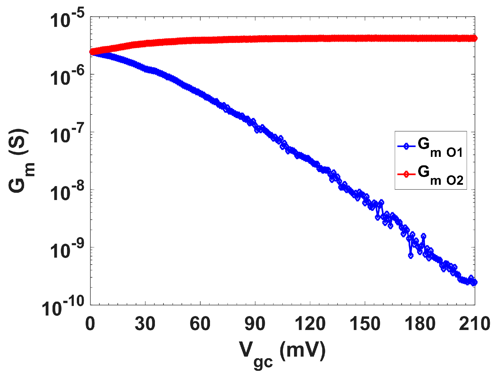
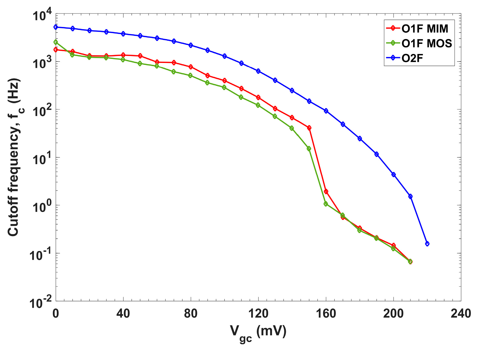
3.2. Gm-C LPF Cutoff Tunability
3.3. DC Input/Output Characteristics
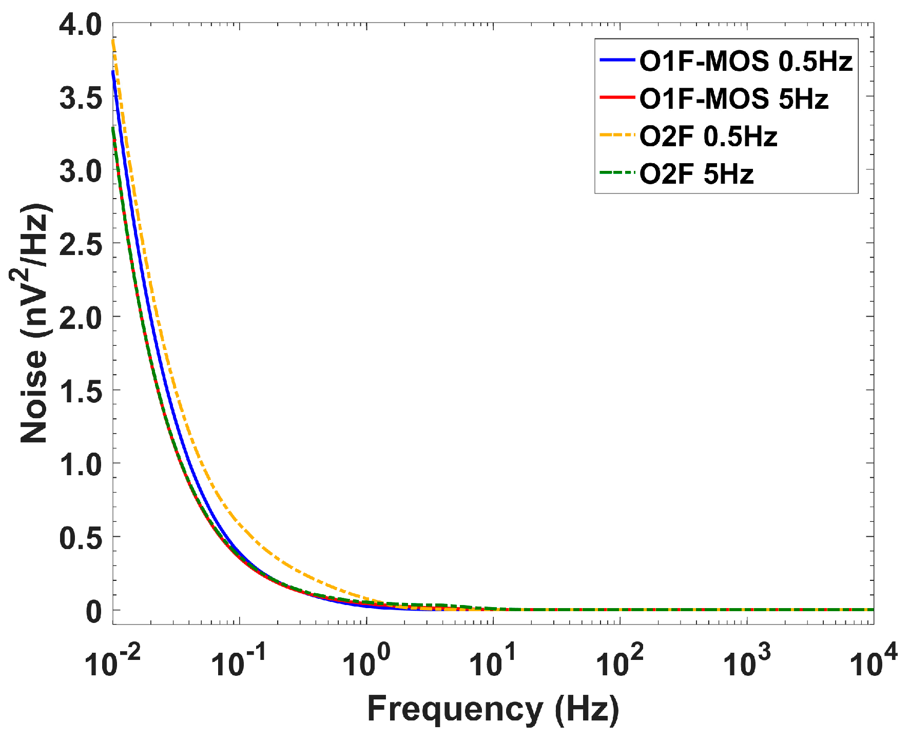
3.4. Dynamic Range
4. LPF in a Lock-In Amplifier
5. Conclusions
Author Contributions
Funding
Acknowledgments
Conflicts of Interest
References
- Wong, A.; Pun, K.P.; Zhang, Y.T.; Hung, K. A Near-Infrared Heart Rate Measurement IC with Very Low Cutoff Frequency Using Current Steering Technique. IEEE TCASI 2005, 52, 2642–2647. [Google Scholar] [CrossRef]
- Rieger, R.; Demosthenous, A.; Taylor, J. A 230-nW 10-s Time Constant CMOS Integrator for an Adaptive Nerve Signal Amplifier. IEEE JSSC 2004, 39, 20–1975. [Google Scholar] [CrossRef]
- Yufera, A.; Rueda, A.; Muñoz, J.M.; Doldan, R.; Leger, G.; Rodriguez-Villegas, E.O. A Tissue Impedance Measurement Chip for Myocardial Ischemia Detection. IEEE TCASI 2005, 52, 2620–2628. [Google Scholar] [CrossRef]
- Li, Y.; Poon, C.C.Y.; Zhang, Y.T. Analog Integrated Circuits Design for Processing Physiological Signals. IEEE R-BME 2010, 3, 93–105. [Google Scholar] [CrossRef]
- Li, H.; Liu, X.; Li, L.; Mu, X.; Genov, R.; Mason, A.J. CMOS Electrochemical Instrumentation for Biosensor Microsystems: A Review. Sensors 2017, 17, 74. [Google Scholar] [CrossRef]
- Shaikh, M.O.; Srikanth, B.; Zhu, P.-Y.; Chuang, C.-H. Impedimetric Immunosensor Utilizing Polyaniline/Gold Nanocomposite-Modified Screen-Printed Electrodes for Early Detection of Chronic Kidney Disease. Sensors 2019, 19, 3990. [Google Scholar] [CrossRef]
- Fernández, A.O.; Pinatti, C.A.O.; Peris, R.M.; Laguarda-Miró, N. Freeze-Damage Detection in Lemons Using Electrochemical Impedance Spectroscopy. Sensors 2019, 19, 4051. [Google Scholar] [CrossRef]
- Ortiz-Aguayo, D.; del Valle, M. Label-Free Aptasensor for Lysozyme Detection Using Electrochemical Impedance Spectroscopy. Sensors 2018, 18, 354. [Google Scholar] [CrossRef]
- Liu, X.; Jiang, H. Construction and Potential Applications of Biosensors for Proteins in Clinical Laboratory Diagnosis. Sensors 2017, 17, 2805. [Google Scholar] [CrossRef]
- Wu, J.; Dong, M.; Santos, S.; Rigatto, C.; Liu, Y.; Lin, F. Lab-on-Chip Platforms for Detection of Cardiovascular Disease and Cancer Biomarkers. Sensors 2017, 17, 2934. [Google Scholar] [CrossRef]
- Qiao, G.; Wang, W.; Duan, W.; Zheng, F.; Sinclair, A.J.; Chatwin, C.R. Bioimpedance Analysis for the Characterization of Breast Cancer Cells in Suspension. IEEE Trans. Biomed. Eng. 2012, 59, 2321–2329. [Google Scholar] [CrossRef] [PubMed]
- Cardoso, A.R.; Cabral-Miranda, G.; Reyes-Sandoval, A.; Bachmann, M.F.; Sales, M.G.F. Detecting circulating antibodies by controlled surface modification with specific target proteins: Application to malaria. Biosens. Bioelectron. 2017, 91, 833–841. [Google Scholar] [CrossRef] [PubMed]
- Badets, F.; Coutard, J.-G.; Russo, P.; Dina, E.; Glière, A.; Nicoletti, S. A 1.3 mW, 12-bit Lock-In Amplifier Based Readout Circuit Dedicated to Photo-Acoustic Gas Sensing. In Proceedings of the IEEE Sensors 2016, Orlando, FL, USA, 30 October–3 November 2016; pp. 1–3. [Google Scholar]
- About Lock-in Amplifiers. Appl. Notes No. 3, Stanford Research System, Data Sheets. 1999. Available online: https://www.thinksrs.com/downloads/PDFs/ApplicationNotes/AboutLIAs.pdf (accessed on 24 November 2019).
- Meade, M.L. Lock-in Amplifiers: Principles and Applications; Peter Peregrinus Ltd.: London, UK, 1983; Available online: https://sites.google.com/site/lockinamplifiers/ (accessed on 24 November 2019).
- Blair, D.P. Phase sensitive detection as a means to recover signals buried in noise. J. Phys. E Sci. Instrum. 1975, 8, 621–627. [Google Scholar] [CrossRef]
- Scofield, J.H. Frequency-domain description of a lock-in amplifier. Am. J. Phys. 1994, 62, 129–133. [Google Scholar] [CrossRef]
- Márquez, A.; Pérez-Bailón, J.; Calvo, B.; Medrano, N. A CMOS Self-Contained Quadrature Signal Generator for SoC Impedance Spectroscopy. Sensors 2018, 18, 1382. [Google Scholar] [CrossRef] [PubMed]
- De Marcellis, A.; Ferri, G.; D’Amico, A. One-Decade Frequency Range, in-Phase Auto-Aligned 1.8 V 2 mW Fully Analog CMOS Integrated Lock-in Amplifier for Small/Noisy Signal Detection. IEEE Sens. J. 2016, 16, 5690–5701. [Google Scholar] [CrossRef]
- Valente, V.; Demosthenous, A. Wideband Fully-Programmable Dual-Mode CMOS Analogue Front-End for Electrical Impedance Spectroscopy. Sensors 2016, 16, 1159. [Google Scholar] [CrossRef]
- Maya-Hernández, P.M.; Sanz-Pascual, M.T.; Calvo, B. Ultralow-Power Synchronous Demodulation for Low-Level Sensor Signal Detection. IEEE TIM 2018, 68, 3514–3523. [Google Scholar] [CrossRef]
- Gosselin, B.; Sawan, M.; Kerherve, E. Linear-Phase Delay Filters for Ultra-Low-Power Signal Processing in Neural Recording Implants. IEEE TBIOCAS 2010, 4, 171–180. [Google Scholar] [CrossRef]
- Peng, S.-Y.; Lee, Y.-H.; Wang, T.-Y.; Huang, H.-C.; Lai, M.-R.; Lee, C.-H.; Liu, L.-H. A Power-Efficient Reconfigurable OTA-C Filter for Low-Frequency Biomedical Applications. IEEE TCASI 2018, 65, 543–555. [Google Scholar] [CrossRef]
- Lu, J.; Yang, T.; Jahan, M.S.; Holleman, J. A low-power 84-dB dynamic-range tunable Gm-C filter for bio-signal acquisition. In Proceedings of the IEEE 57th International Midwest Symposium on Circuits and Systems (MWSCAS), College Station, TX, USA, 3–6 August 2014; pp. 1029–1032. [Google Scholar]
- Wang, S.; Koickal, T.J.; Hamilton, A.; Cheung, R.; Smith, L.S. A Bio-Realistic Analog CMOS Cochlea Filter with High Tunability and Ultra-Steep Roll-Off. IEEE TBIOCAS 2015, 9, 297–311. [Google Scholar]
- Rodriguez, S.; Ollmar, S.; Waqar, M.; Rusu, A. A Batteryless Sensor ASIC for Implantable Bio-Impedance Applications. IEEE TBIOCAS 2016, 10, 533–544. [Google Scholar] [CrossRef] [PubMed]
- Bruschi, P.; Nizza, N.; Pieri, F.; Schipani, M.; Cardisciani, D. A Fully Integrated Single-Ended 1.5–15-Hz Low-Pass Filter with Linear Tuning Law. IEEE JSSC 2007, 42, 1522–1528. [Google Scholar] [CrossRef]
- Arnaud, A.; Fiorelli, R.; Galup-Montoro, C. Nanowatt, Sub-nS OTAs, with Sub-10-mV Input Offset, Using Series-Parallel Current Mirrors. IEEE JSSC 2006, 41, 2009–2018. [Google Scholar] [CrossRef]
- Veeravalli, A.; Sanchez-Sinencio, E.; Silva-Martinez, J. Transconductance amplifier structures with very small transconductances: A comparative design approach. IEEE JSSC 2002, 37, 770–775. [Google Scholar] [CrossRef]
- Solis-Bustos, S.; Silva-Martinez, J.; Maloberti, F.; Sanchez-Sinencio, E. A 60-dB dynamic-range CMOS sixth-order 2.4-Hz low-pass filter for medical applications. IEEE TCASII 2000, 47, 1391–1398. [Google Scholar] [CrossRef]
- Lee, S.; Wang, C.; Chu, Y. Low-Voltage OTA–C Filter with an Area- and Power-Efficient OTA for Biosignal Sensor Applications. IEEE TBIOCAS 2019, 13, 56–61. [Google Scholar] [CrossRef]
- Sun, C.; Lee, S. A Fifth-Order Butterworth OTA-C LPF with Multiple-Output Differential-Input OTA for ECG Applications. IEEE TCASII 2018, 65, 421–425. [Google Scholar] [CrossRef]
- Sawigun, C.; Thanapitak, S. A 0.9-nW, 101-Hz, and 46.3-µVrms IRN Low-Pass Filter for ECG Acquisition Using FVF Biquads. IEEE TVLSI 2018, 26, 2290–2298. [Google Scholar]
- Germanovix, W.; Bonizzoni, E.; Maloberti, F. Capacitance Super Multiplier for Sub-Hertz Low-Pass Integrated Filters. IEEE TCASII 2018, 65, 301–305. [Google Scholar] [CrossRef]
- Rodriguez-Villegas, E.; Casson, A.J.; Corbishley, P. A sub-Hertz nanopower low pass filter. IEEE TCASII 2011, 58, 351–355. [Google Scholar]
- Sawigun, C.; Serdijn, W.A. A Modular Transconductance Reduction Technique for Very Low-Frequency Gm-C Filters. In Proceedings of the IEEE ISCAS 2012, Seoul, Korea, 20–23 May 2012; pp. 1183–1186. [Google Scholar]
- Pérez-Bailón, J.; Marquez, A.; Calvo, B.; Medrano, N. A 0.18μm CMOS Widely Tunable Low Pass Filter with sub-Hz Cutoff Frequencies. In Proceedings of the IEEE ISCAS 2018, Florence, Italy, 27–30 May 2018. [Google Scholar]
- Geiger, R.L.; Sanchez-Sinencio, E. Active Filter Design Using Operational Transconductance Amplifiers: A Tutorial. IEEE Circ. Devices Mag. 1985, 1, 20–32. [Google Scholar] [CrossRef]
- Ramírez-Angulo, J.; Sudha Gariemlla, S.R.; Lopez-Martin, A. New Gain Programmable Current Mirrors Based on Current Steering. In Proceedings of the IEEE International Midwest Symposium on Circuits and Systems (MWSCAS), San Juan, Puerto Rico, 6–9 August 2006. [Google Scholar]
- Maxim Integrated, MAX5413/14/15. Available online: https://datasheets.maximintegrated.com/en/ds/MAX5413-MAX5415.pdf (accessed on 27 September 2019).
- Maxim Integrated, MAX5520. Available online: https://datasheets.maximintegrated.com/en/ds/MAX5520-MAX5521.pdf (accessed on 27 September 2019).
- Maxim Integrated, MAX5530. Available online: https://datasheets.maximintegrated.com/en/ds/MAX5530-MAX5531.pdf (accessed on 27 September 2019).
- Sharuddin, I.; Lee, L.; Yusof, Z. Analysis design of area efficient segmentation digital to analog converter for ultra-low power successive approximation analog to digital converter. Microelectron. J. 2016, 52, 80–90. [Google Scholar] [CrossRef]
- Gosselin, B.; Simard, V.; Sawan, M. Low power programmable front-end for a multichannel neural recording interface. In Proceedings of the CCECE 2003—Canadian Conference on Electrical and Computer Engineering. Toward a Caring and Humane Technology, Montreal, QC, Canada, 4–7 May 2003; Volume 2, pp. 911–914. [Google Scholar] [CrossRef]
- Pérez-Bailón, J.; Márquez, A.; Calvo, B.; Medrano, N. A 0.18 µm CMOS LDO Regulator for an on-Chip Sensor Array Impedance Measurement System. Sensors 2018, 18, 1405. [Google Scholar] [CrossRef] [PubMed]
- Urbiztondo, M.A.; Peralta, A.; Pellejero, I.; Sese, J.; Pina, M.P.; Dufour, I.; Santamaria, J. Detection of organic vapours with Si cantilevers coated with inorganic (zeolites) for organic (polymer) layers. Sens. Actuators B Chem. 2012, 171–172, 822–831. [Google Scholar] [CrossRef]
- Sánchez-Rodríguez, T.; Gomez-Galan, J.A.; Carvajal, R.G.; Sánchez-Raya, M.; Muñoz, F.; Ramírez-Angulo, J. A 1.2-V 450-μW Gm-C Bluetooth Channel Filter Using a Novel Gain-Boosted Tunable Transconductor. IEEE TVLSI 2015, 23, 1572–1576. [Google Scholar]


| Parameter | O1F | O2F | [24] ‘14 | [25] ‘15 | [47] ‘15 | [33] ‘18 | [32] ‘18 | [23] ‘18 |
|---|---|---|---|---|---|---|---|---|
| Technology (µm) | 0.18 | 0.18 | 0.6 | 0.35 | 0.13 | 0.35 | 0.18 | 0.35 |
| Vsupply (V) | 1.8 | 1.8 | 3.3 | 3.3 | 1.2 | 0.6 | 1 | 1.8 |
| IBias (nA) | 500 | 500 | NA | NA | NA | 1.5–4.5 | NA | 14.9–182.3 |
| Power (µW) | 5.4 | 9.9 | 75.9 | 59.5–90 | 450 | 9–27(10−4) | 0.35 | 0.1–1.31 |
| Order | 1 | 2 | 2 | 9 | 3 | 4 | 5 | 2 |
| Gain (dB) | <0.5 | <0.5 | ≈0 | 18.8/21.1@fc | 10 | −2.77 | −6/−8 | 0–12 |
| Area (mm2) | 0.0140 | 0.0264 | 0.17 | 0.9 | 0.08 | 0.168 | 0.12 | 0.12 |
| T range (°C) | −40 to 100 | −40 to 100 | NA | NA | NA | NA | NA | NA |
| DC in/out range (V) | 0.39(0.45 **)–1.65 | 0.45–1.65 | NA | NA | NA | NA | NA | NA |
| fc (Hz) | 0.066–2.5 k | 0.157–5.2 k | 2.5 k–10 k | 31–8 k | 375 k–590 k | 101–272 | 50 | 2 k–20 k |
| noise (µVrms) | 13.3; 16.3(a,b) | 19.2; 19.9(a,b) | 91.8; 60.7 | 93.3; 34.3(c) | 342 | 46.6; 46.8 | 100 | 86.3; 84.3 |
| Vpp@THD≤1% | 0.22; 0.16(a) | 0.305; 0.345(a) | 4.13; 3.13 | 0.082; 0.031(d) | 0.45 | NA | NA | 0.216; 0.294 |
| DR (dB) | 75.3; 70.9(a) | 75; 75.7(a) | 84–85.2 | 49.8–50.2 | 53.35 | 47 | 49.9 | 58.9; 61.8 |
| NP (µ) | 1.07 | 1.96 | NA | 3.34–5.05 | NA | NA | 0.292 | 0.02–0.3 |
| Normalized Area | 0.432 | 0.815 | 0.472 | 7.347 | 4.734 | 1.371 | 3.704 | 0.980 |
| FoM1 (10−10) | 1.838–3.051 | 1.743–1.608 | NA | 12–17.34 | NA | NA | 1.868 | 0.114–1.219 |
| FoM2 (µ) | 2.64*10−5–1.66 | 1.126 × 10⁻⁴–3.44 | 2.83–9.84 | 4.87–1.816 × 10³ | 0.573 × 10⁶–0.9 × 10⁶ | 1.39 × 10⁻⁴–1.12 × 10⁻³ | 0.0415 | 0.11–10.4 |
© 2019 by the authors. Licensee MDPI, Basel, Switzerland. This article is an open access article distributed under the terms and conditions of the Creative Commons Attribution (CC BY) license (http://creativecommons.org/licenses/by/4.0/).
Share and Cite
Pérez-Bailón, J.; Calvo, B.; Medrano, N. A CMOS Low Pass Filter for SoC Lock-in-Based Measurement Devices. Sensors 2019, 19, 5173. https://doi.org/10.3390/s19235173
Pérez-Bailón J, Calvo B, Medrano N. A CMOS Low Pass Filter for SoC Lock-in-Based Measurement Devices. Sensors. 2019; 19(23):5173. https://doi.org/10.3390/s19235173
Chicago/Turabian StylePérez-Bailón, Jorge, Belén Calvo, and Nicolás Medrano. 2019. "A CMOS Low Pass Filter for SoC Lock-in-Based Measurement Devices" Sensors 19, no. 23: 5173. https://doi.org/10.3390/s19235173
APA StylePérez-Bailón, J., Calvo, B., & Medrano, N. (2019). A CMOS Low Pass Filter for SoC Lock-in-Based Measurement Devices. Sensors, 19(23), 5173. https://doi.org/10.3390/s19235173