A Differential Resonant Voltage Sensor Consisting of Piezo Bimorph and Quartz Crystal Double-Ended Tuning Fork Resonators


Abstract
:1. Introduction
2. The Principle and Configuration of the Differential Resonant Voltage Sensor
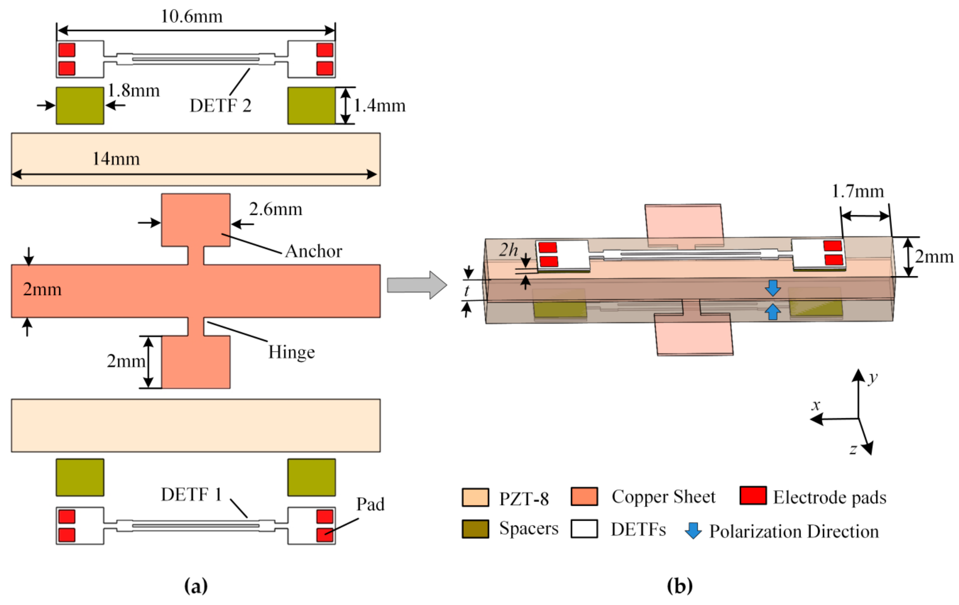
2.1. Design and Configuration of the Device
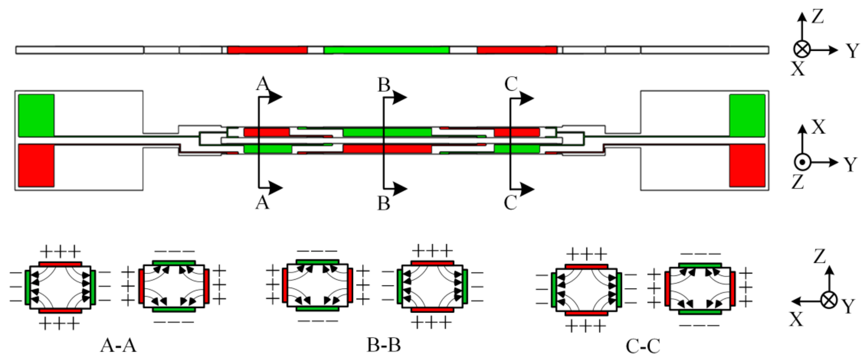
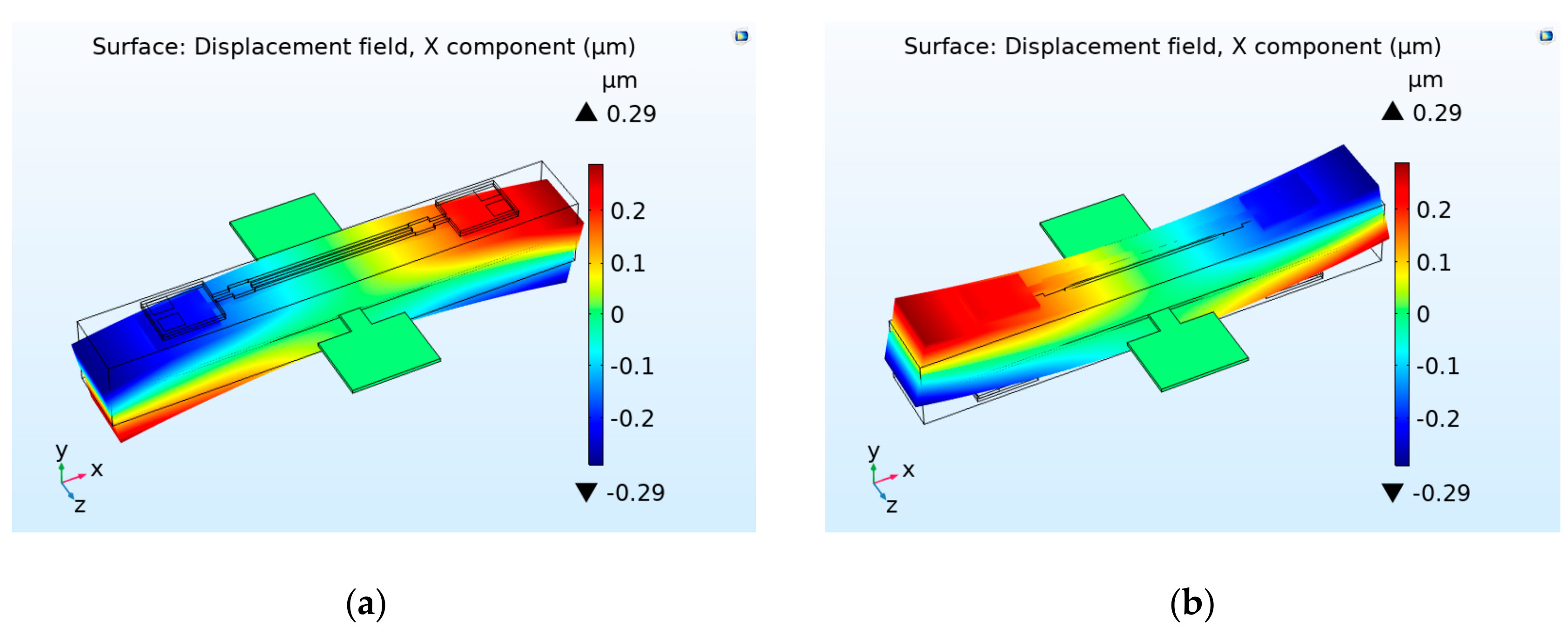
2.2. Theoretical Analysis and Simulation
3. Device Fabrication and Experiments
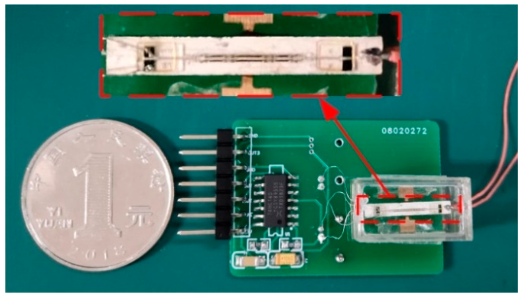
3.1. Fabrication of the Device
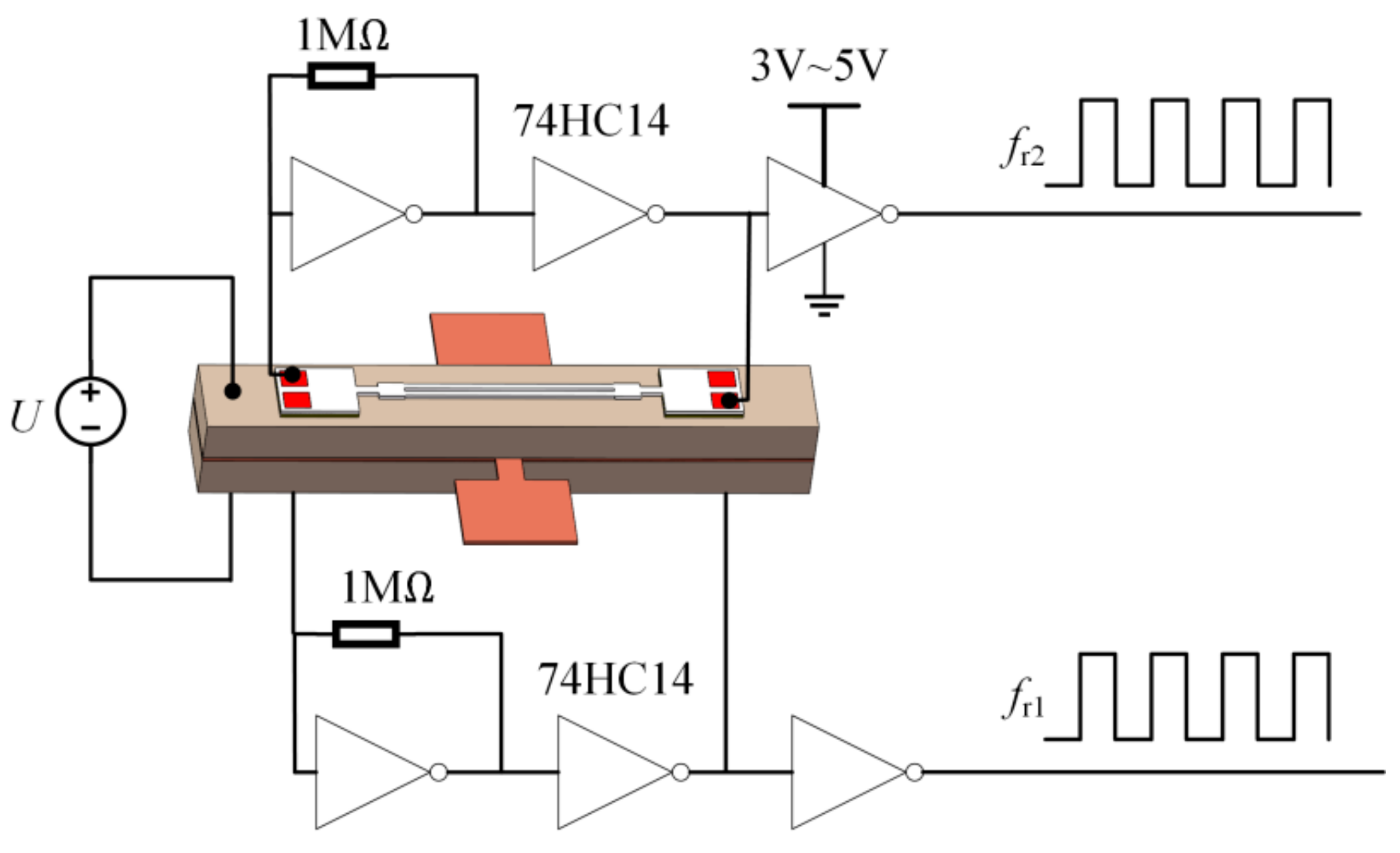
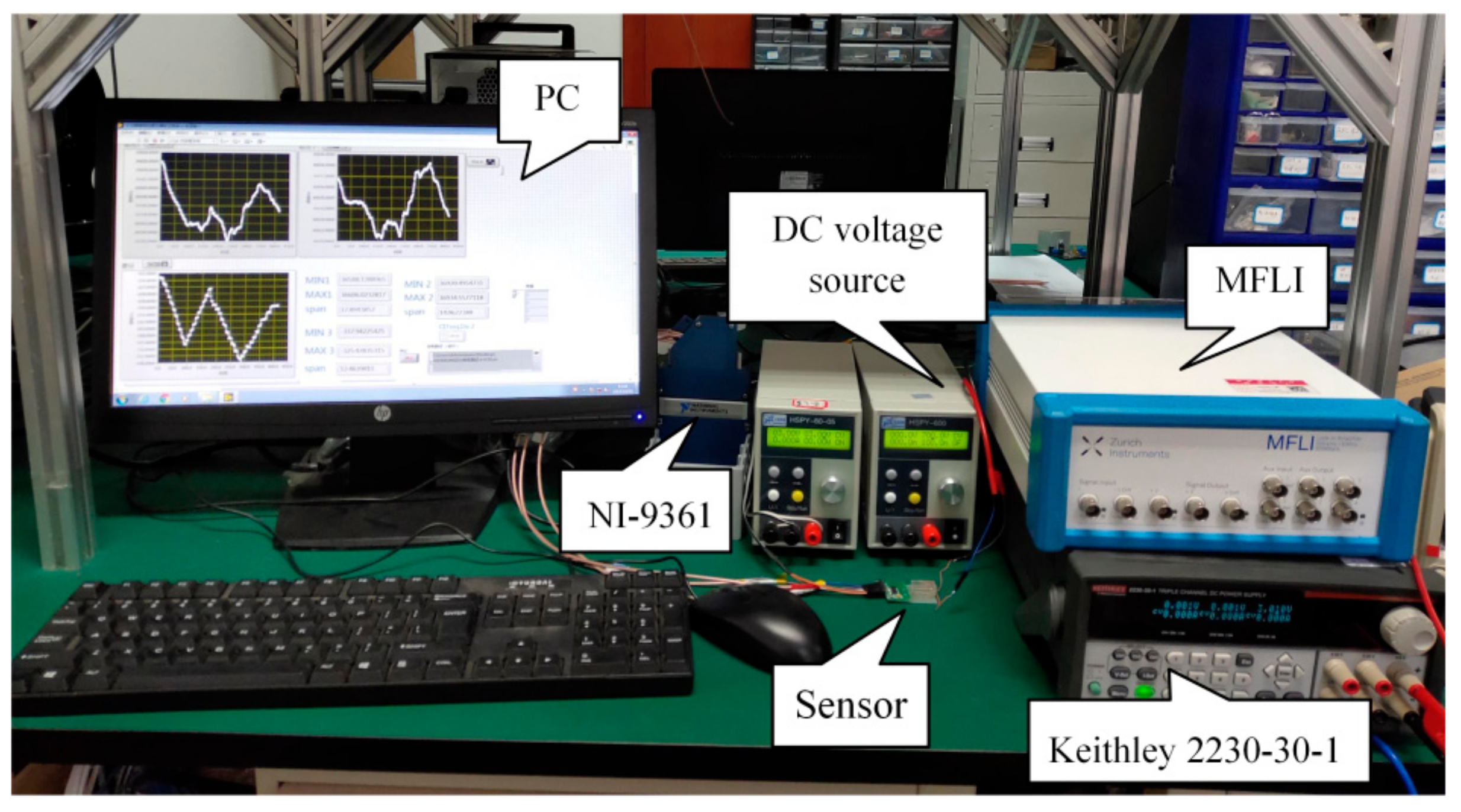
3.2. Experimental Setup
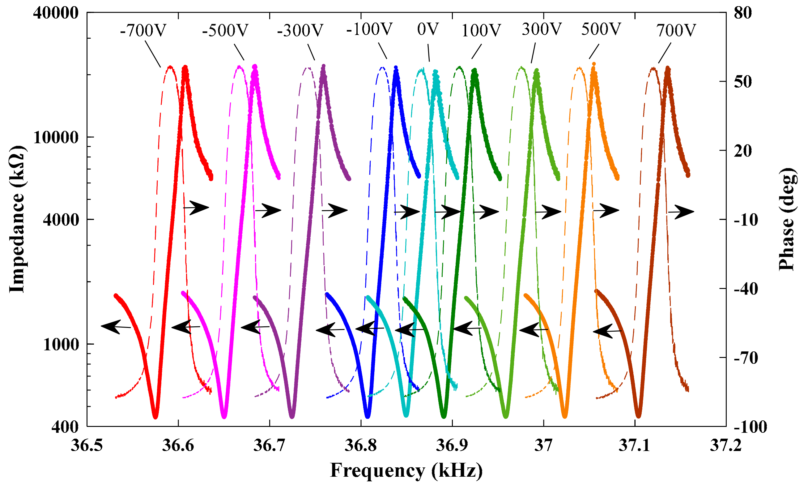
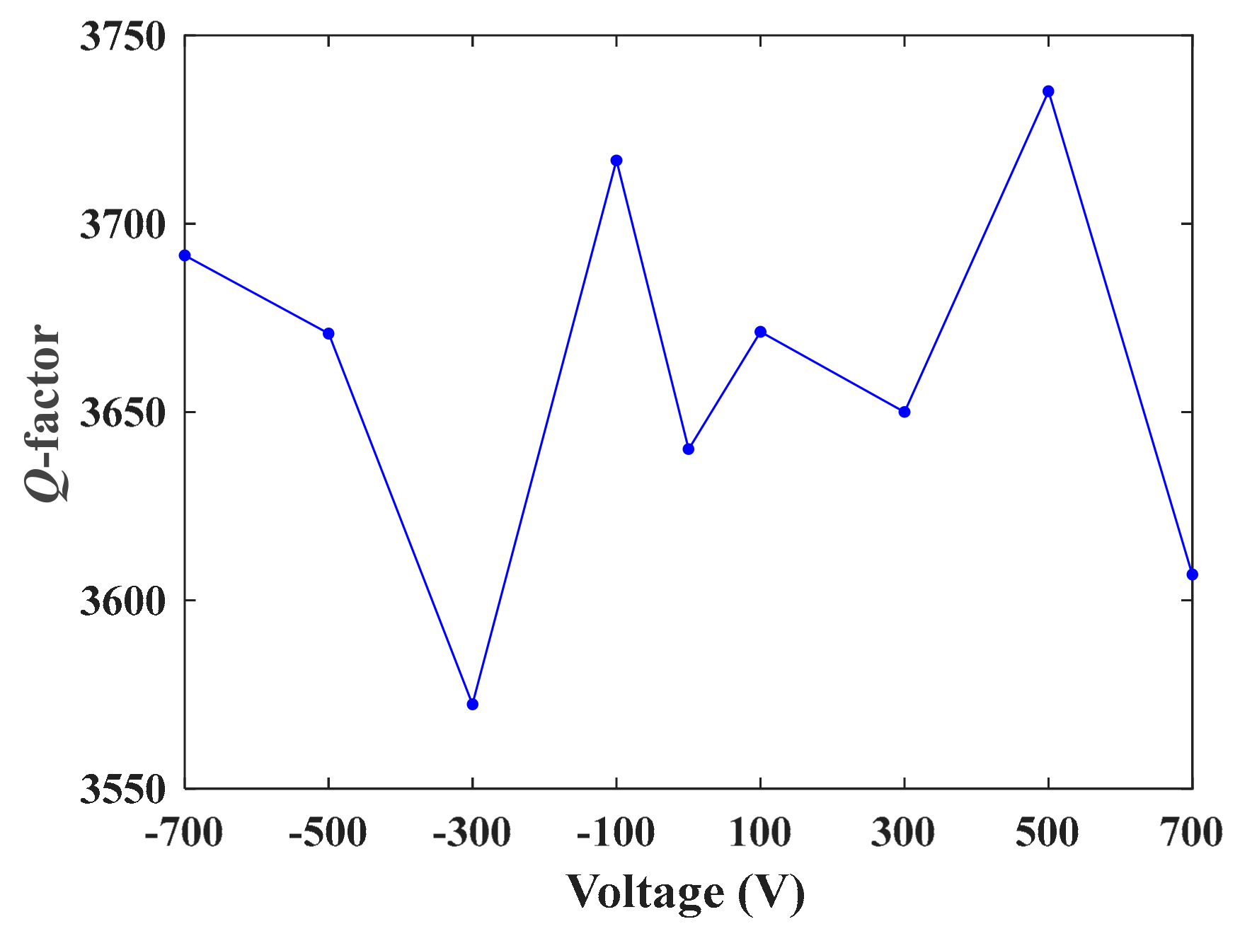
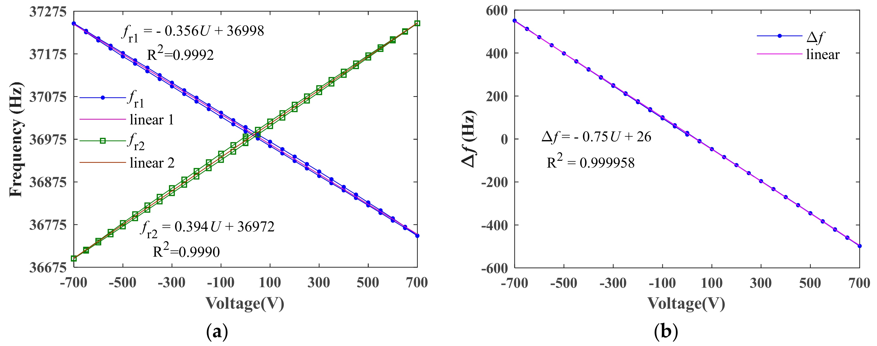
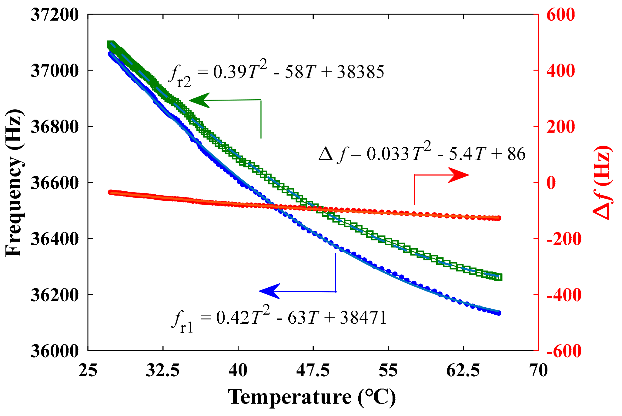
4. Results and Discussions
5. Conclusions
Author Contributions
Funding
Conflicts of Interest
Appendix A

| 0 C/N | 0 C/N | 0 C/N | 0 C/N | 0 C/N | |
|---|---|---|---|---|---|
| 0 C/N | 0 C/N | 0 C/N | C/N | 0 C/N | 0 C/N |
| C/N | C/N | C/N | 0 C/N | 0 C/N | 0 C/N |
| 147 GPa | 81 GPa | 81 GPa | 0 GPa | 0 GPa | 0 GPa |
| 81 GPa | 147 GPa | 81 GPa | 0 GPa | 0 GPa | 0 GPa |
| 81 GPa | 81 GPa | 147 GPa | 0 GPa | 0 GPa | 0 GPa |
| 0 GPa | 0 GPa | 0 GPa | 147 GPa | 0 GPa | 0 GPa |
| 0 GPa | 0 GPa | 0 GPa | 0 GPa | 147 GPa | 0 GPa |
| 0 GPa | 0 GPa | 0 GPa | 0 GPa | 0 GPa | 147 GPa |
References
- Leirbukt, A.; Uhlen, K.; Palsson, M.T.; Gjerde, J.O.; Vu, K.; Kirkeluten, O. Voltage monitoring and control for enhanced utilization of power grids. In Proceedings of the IEEE PES Power Systems Conference and Exposition, New York, NY, USA, 10–13 October 2004. [Google Scholar]
- Femine, A.D.; Gallo, D.; Landi, C.; Schiavo, A.L.; Luiso, M. Low Power Contacless Voltage Sensor for IoT Applications. In Proceedings of the 2019 II Workshop on Metrology for Industry 4.0 and IoT (MetroInd4. 0&IoT), Naples, Italy, 4–6 June 2019. [Google Scholar]
- Wang, D.; He, R.; Han, J.; Fattouche, M.; Ghannouchi, F.M. Sensor Network Based Oilwell Health Monitoring and Intelligent Control. IEEE Sens. J. 2012, 12, 1326–1339. [Google Scholar] [CrossRef]
- Chen, Y.C.; Hsu, W.H.; Cheng, S.H.; Cheng, Y.T. A flexible, non-intrusive power sensor tag for the electricity monitoring of two-wire household appliances. In Proceedings of the 2012 IEEE 25th International Conference on Micro Electro Mechanical Systems (MEMS), Paris, France, 29 January–2 February 2012. [Google Scholar]
- Kaczmarek, M.; Szatilo, T. Reference voltage divider designed to operate with oscilloscope to enable determination of ratio error and phase displacement frequency characteristics of MV voltage transformers. Measurement 2015, 68, 22–31. [Google Scholar] [CrossRef]
- Zhang, C.X.; Feng, X.; Liang, S.; Zhang, C.Y.; Li, C. Quasi-reciprocal reflective optical voltage sensor based on Pockels effect with digital closed-loop detection technique. Opt. Commun. 2010, 283, 3878–3883. [Google Scholar] [CrossRef]
- Hebner, R.E.; Cassidy, E.C.; Jones, J.E. Improved Techniques for the Measurement of High-Voltage Impulses Using the Electrooptic Kerr Effect. IEEE Trans. Instrum. Meas. 1975, 24, 361–366. [Google Scholar] [CrossRef]
- Allil, R.C.D.S.B.; Werneck, M.M. Optical High-Voltage Sensor Based on Fiber Bragg Grating and PZT Piezoelectric Ceramics. IEEE Trans. Instrum. Meas. 2011, 60, 2118–2125. [Google Scholar] [CrossRef]
- Xue, F.; Hu, J.; Guo, Y.; Han, G.; Ouyang, Y.; Wang, S.; He, J. Piezoelectric-piezoresistive Coupling MEMS Sensors for Measurement of Electric Fields of Broad Bandwidth and Large Dynamic Range. IEEE Trans. Ind. Electron. 2019, 67, 551–559. [Google Scholar] [CrossRef]
- Nobunaga, N.; Hasegawa, S.; Kumagai, S.; Masuno, K.; Ishii, M.; Uematsu, S.; Sasaki, M. Isolated voltage sensing using micro-resonator. In Proceedings of the 2013 Transducers & Eurosensors XXVII: The 17th International Conference on Solid-State Sensors, Actuators and Microsystems (TRANSDUCERS & EUROSENSORS XXVII), Barcelona, Spain, 16–20 June 2013. [Google Scholar]
- Wada, Y.; Nobunaga, N.; Kumagai, S.; Ishihara, H.; Ishii, M.; Sasako, M. MEMS Resonator-Based Insulated Voltage Sensor Withstanding Higher Voltage. Electr. Eng. Jpn. 2018, 203, 58–64. [Google Scholar] [CrossRef]
- Wang, Q.M.; Du, X.H.; Xu, B.; Cross, L.E. Electromechanical coupling and output efficiency of piezoelectric bending actuators. IEEE Trans. Ultrason. Ferroelectr. Freq. Control 1999, 46, 638–646. [Google Scholar] [CrossRef] [PubMed]
- Bian, L.; Wen, Y.; Wu, Y.; Li, P.; Wu, Z.; Jia, Y.; Zhu, Z. A resonant magnetic field sensor with high quality factor based on quartz crystal resonator and magnetostrictive stress coupling. IEEE Trans. Electron Devices 2018, 65, 2585–2591. [Google Scholar] [CrossRef]
- Fukuzawa, K.; Ando, T.; Shibamoto, M.; Mitsuya, Y.; Zhang, H. Monolithically fabricated double-ended tuning-fork-based force sensor. J. Appl. Phys. 2006, 99, 094901. [Google Scholar] [CrossRef]
- Inman, D.J.; Cudney, H.H. Structural and Machine Design Using Piezoceramic Materials: A Guide for Structural Design Engineers; NASA Langley Research Center: Hampton, VA, USA, 2000; pp. 39–44. [Google Scholar]
- Li, C.; Zhao, Y.L.; Cheng, R.J.; Yu, Z.L.; Liu, Y. A resonant sensor composed of quartz double ended tuning fork and silicon substrate for digital acceleration measurement. Rev. Sci. Instrum. 2014, 85, 035004. [Google Scholar] [CrossRef] [PubMed]
- Bian, L.; Wen, Y.; Li, P. Composite Magnetoelectric Transducer of Terfenol-D and Pb(Zr, Ti)O3 Plates Bonded on an Elastic Substrate. IEEE Sens. J. 2008, 9, 45–50. [Google Scholar] [CrossRef]
- Fang, D.; Li, C. Nonlinear electric-mechanical behavior of a soft PZT-51 ferroelectric ceramic. J. Mater. Sci. 1999, 34, 4001–4010. [Google Scholar] [CrossRef]
- Xu, Q. Identification and Compensation of Piezoelectric Hysteresis without Modeling Hysteresis Inverse. IEEE Trans. Ind. Electron. 2013, 60, 3927–3937. [Google Scholar] [CrossRef]


| Description | Value |
|---|---|
| Length of tine | 4.8 mm |
| Width of tine | 0.146 mm |
| Thickness of tine | 0.1 mm |
| Interval between the tines | 0.1 mm |
| Total length of the DETF | 10.6 mm |
| Length and width of the supporting parts of DETF | 1.8 mm 1.4 mm |
| E (GPa) | ρ (kg/m3) | d31 (×10−12 C/N) | εr | ρR (Ω m) | |
|---|---|---|---|---|---|
| PZT-8 | 147 | 7600 | −97 | ~1000 | 1010 |
| Quartz crystal | 86 | 2650 |
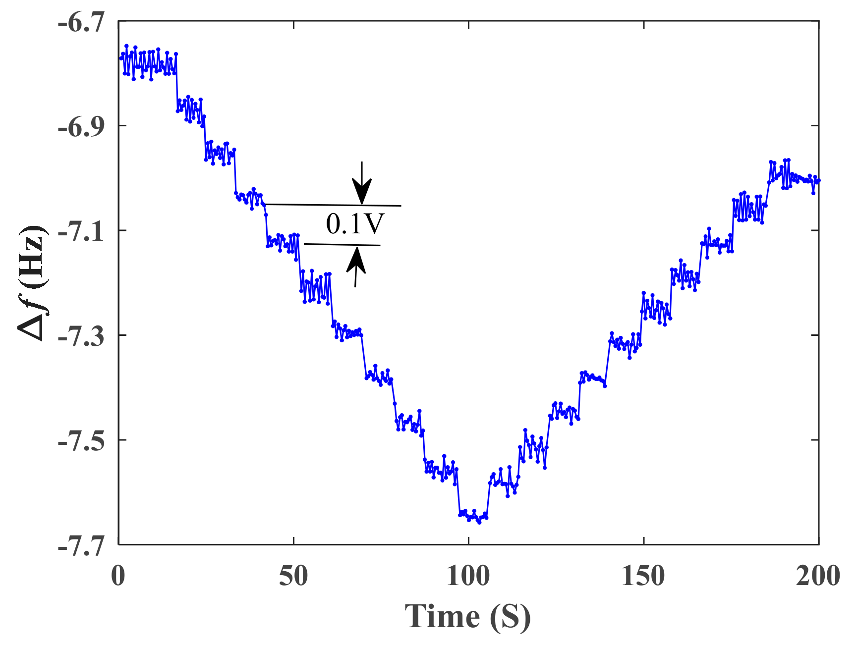
| Step i | (Hz) | (Hz) | (Hz) | (Hz) | |||
|---|---|---|---|---|---|---|---|
| 0 | −6.78 | - | 0 | 11 | −7.58 | 0.065 | 0.9 |
| 1 | −6.87 | 0.089 | 0.1 | 12 | −7.52 | 0.063 | 0.8 |
| 2 | −6.95 | 0.081 | 0.2 | 13 | −7.44 | 0.068 | 0.7 |
| 3 | −7.04 | 0.087 | 0.3 | 14 | −7.38 | 0.065 | 0.6 |
| 4 | −7.12 | 0.084 | 0.4 | 15 | −7.32 | 0.066 | 0.5 |
| 5 | −7.20 | 0.085 | 0.5 | 16 | −7.25 | 0.064 | 0.4 |
| 6 | −7.29 | 0.083 | 0.6 | 17 | −7.19 | 0.063 | 0.3 |
| 7 | −7.38 | 0.087 | 0.7 | 18 | −7.17 | 0.062 | 0.2 |
| 8 | −7.47 | 0.087 | 0.8 | 19 | −7.06 | 0.068 | 0.1 |
| 9 | −7.55 | 0.086 | 0.9 | 20 | −7.00 | 0.059 | 0 |
| 10 | −7.65 | 0.092 | 1.0 |
| Parameter | Value | As % of Full Scale |
|---|---|---|
| Q-factor (in air ) | ~3661 | |
| Measurement range | ±700 V | |
| Differential Frequency shift (for ±700 V) | 1049 Hz | |
| Sensitivity | 0.75 Hz/V | |
| Resolution | 0.1 V | 0.007 |
| Max hysteresis | 8 Hz | 0.76 |
| Max non-linearity | 3 Hz | 0.29 |
| Input impedance | >714 GΩ//~124 pF | |
| Power consumption | 150 μW (3 V, 50 μA) |
© 2019 by the authors. Licensee MDPI, Basel, Switzerland. This article is an open access article distributed under the terms and conditions of the Creative Commons Attribution (CC BY) license (http://creativecommons.org/licenses/by/4.0/).
Share and Cite
Huang, Z.; Bian, L. A Differential Resonant Voltage Sensor Consisting of Piezo Bimorph and Quartz Crystal Double-Ended Tuning Fork Resonators. Sensors 2019, 19, 5031. https://doi.org/10.3390/s19225031
Huang Z, Bian L. A Differential Resonant Voltage Sensor Consisting of Piezo Bimorph and Quartz Crystal Double-Ended Tuning Fork Resonators. Sensors. 2019; 19(22):5031. https://doi.org/10.3390/s19225031
Chicago/Turabian StyleHuang, Zijun, and Leixiang Bian. 2019. "A Differential Resonant Voltage Sensor Consisting of Piezo Bimorph and Quartz Crystal Double-Ended Tuning Fork Resonators" Sensors 19, no. 22: 5031. https://doi.org/10.3390/s19225031
APA StyleHuang, Z., & Bian, L. (2019). A Differential Resonant Voltage Sensor Consisting of Piezo Bimorph and Quartz Crystal Double-Ended Tuning Fork Resonators. Sensors, 19(22), 5031. https://doi.org/10.3390/s19225031