Parasitics Impact on the Performance of Rectifier Circuits in Sensing RF Energy Harvesting


 , ,
, ,  and
and
Abstract
:1. Introduction
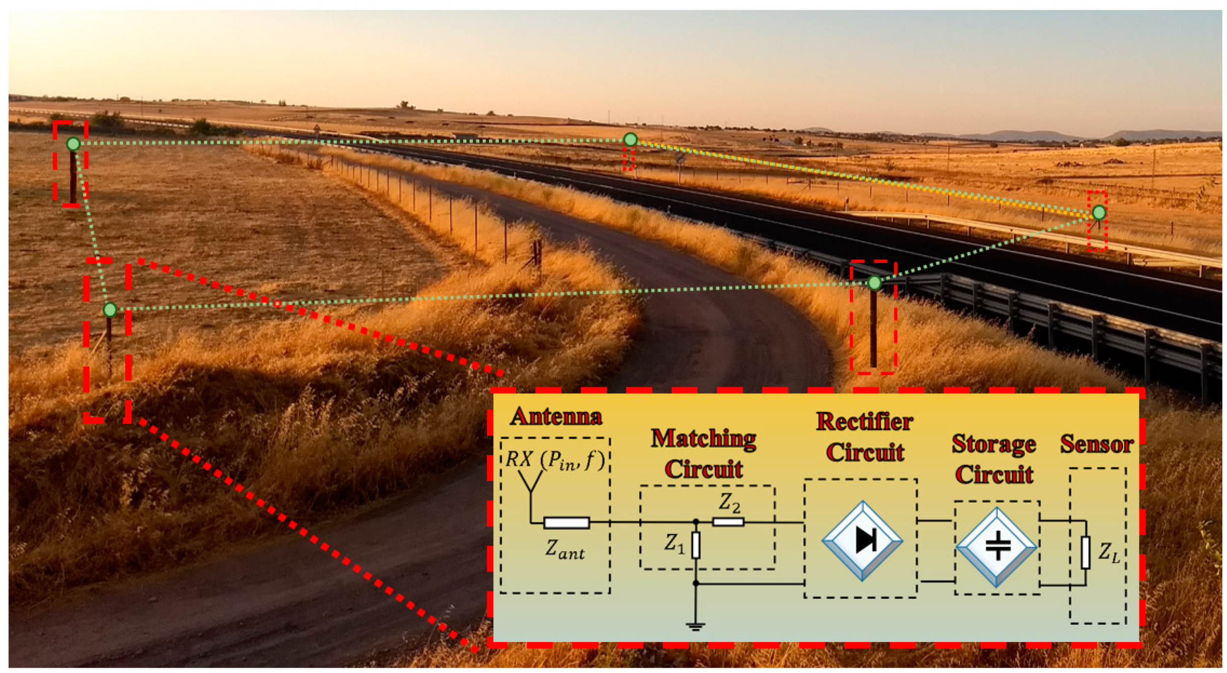
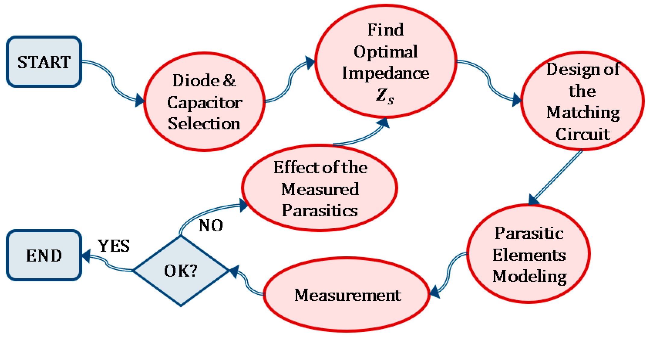
2. Design Process
3. Choice of Components
4. Circuit Design
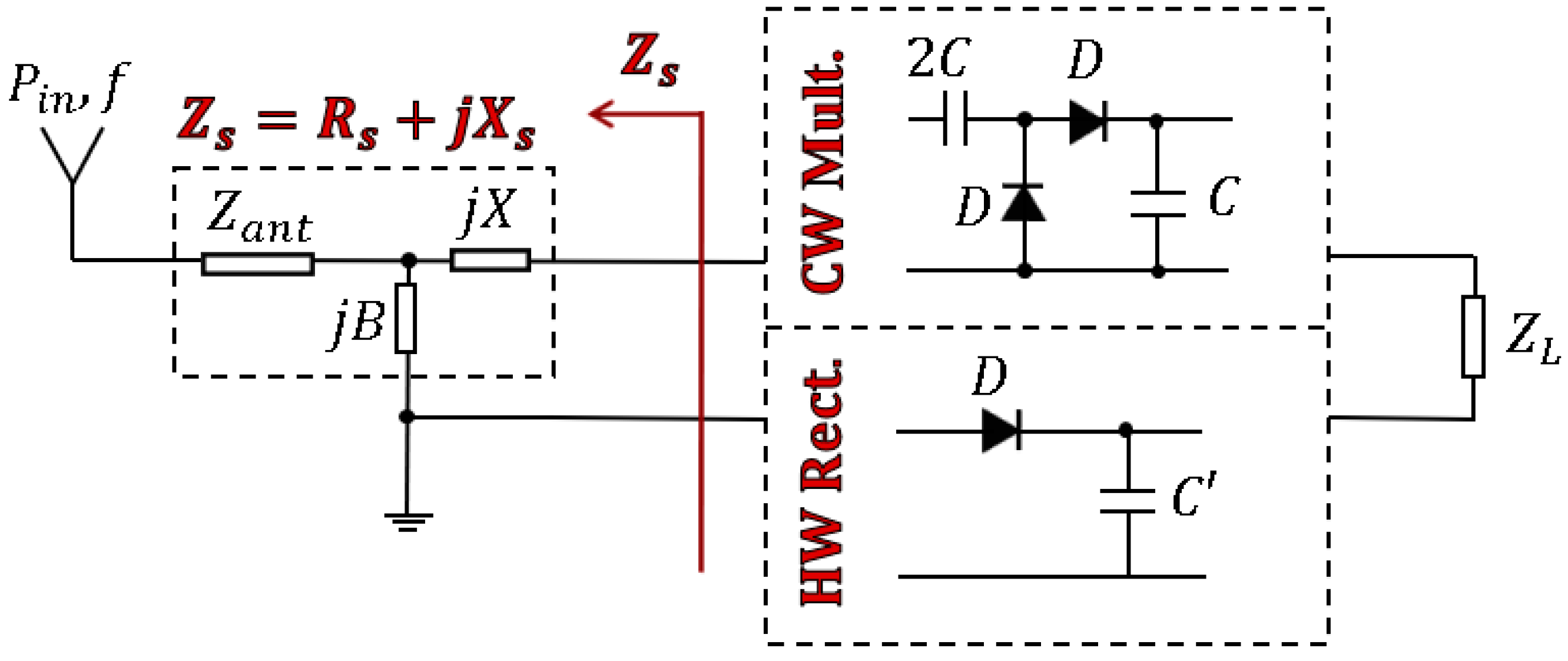
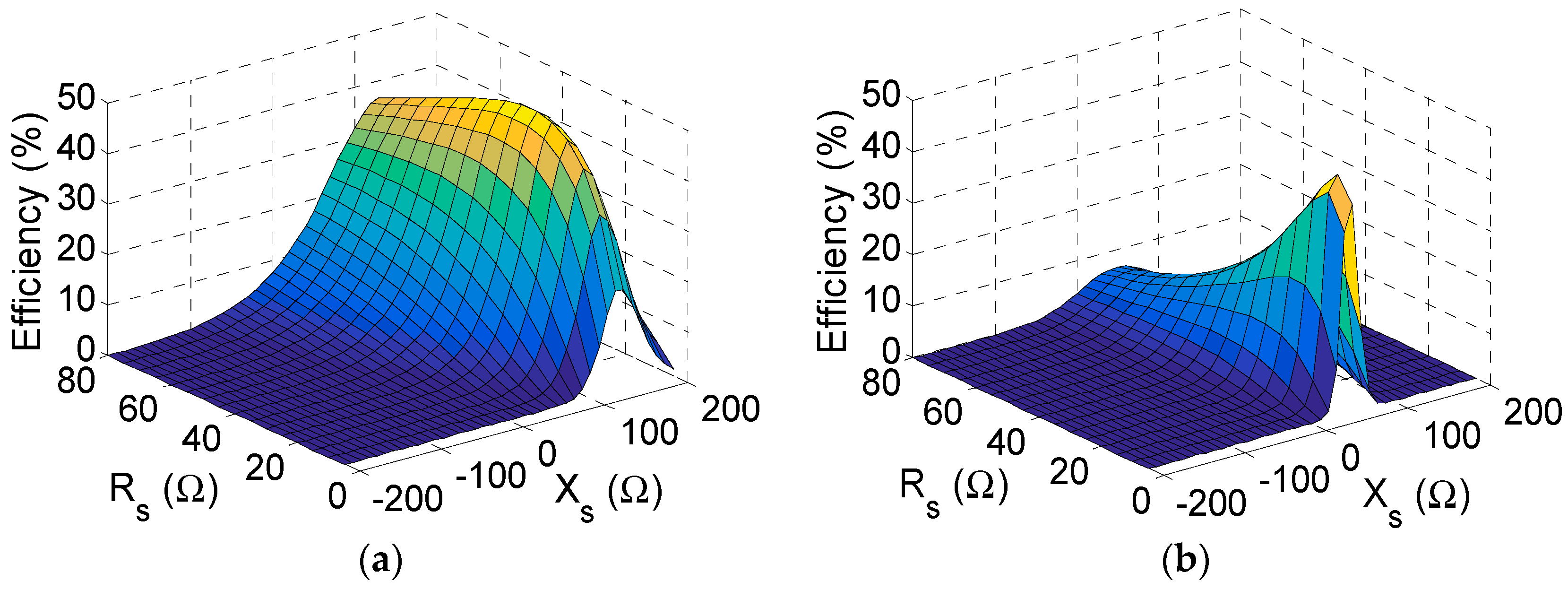
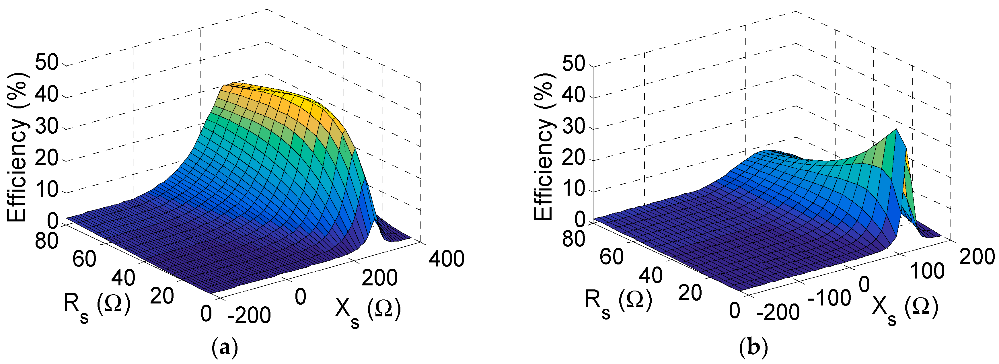
Optimal Source Impedance
5. Parasitic Elements
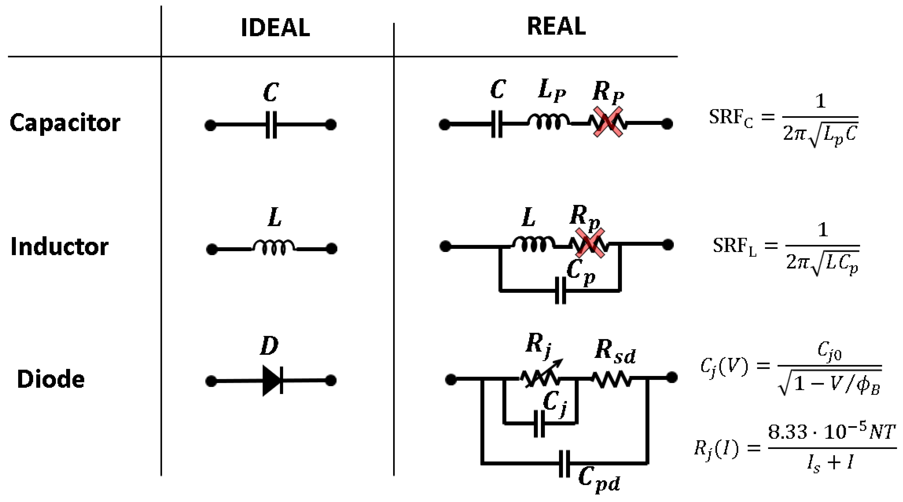
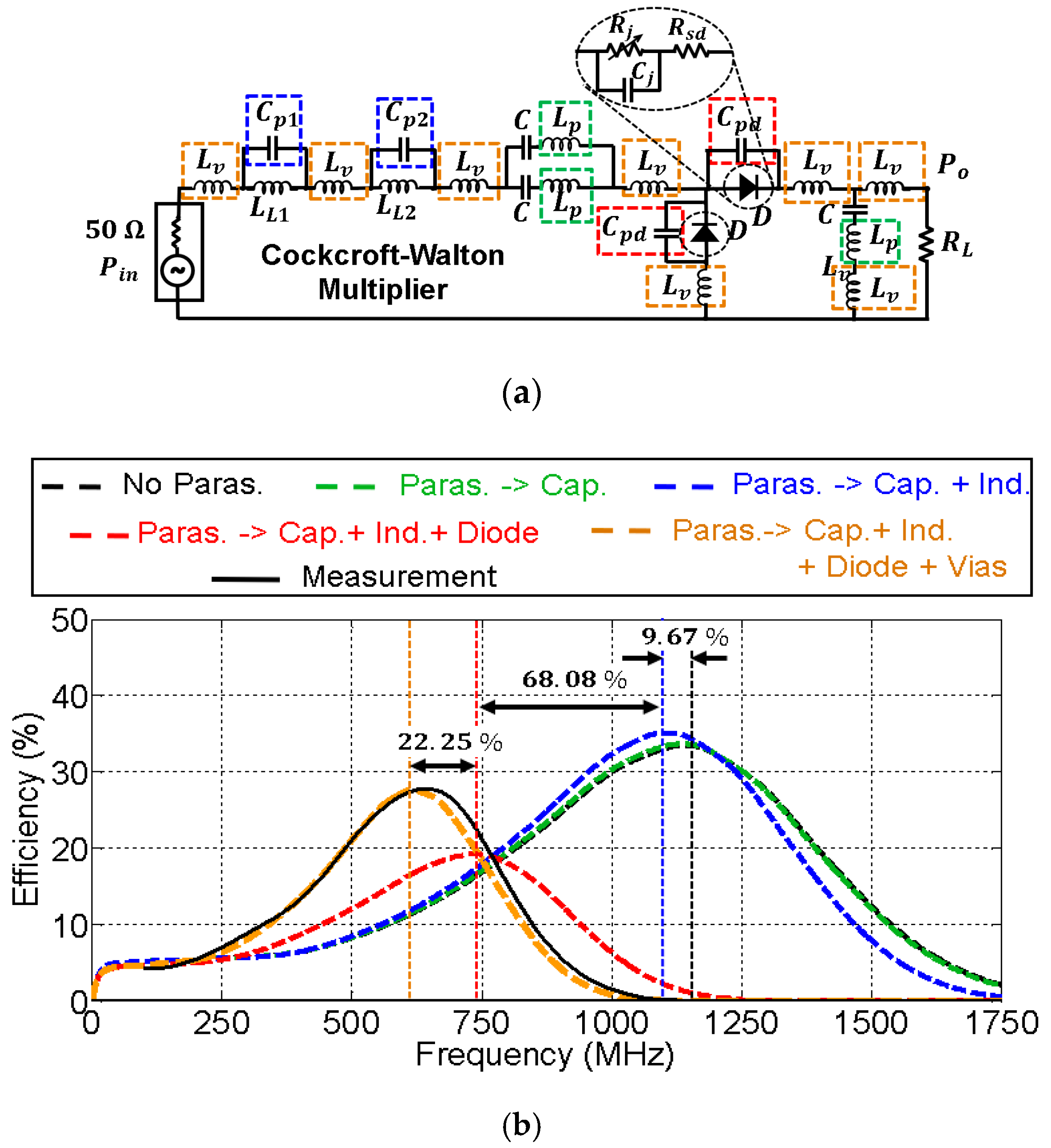
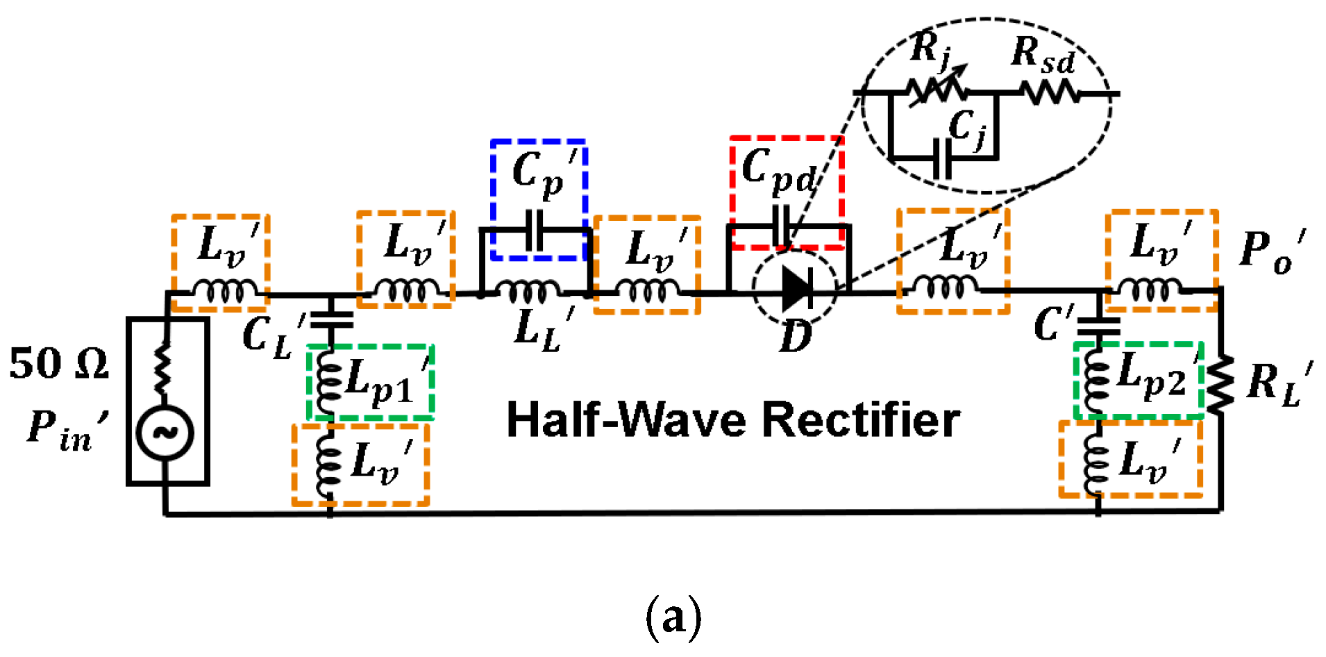
5.1. Circuit Model
5.2. Discussion
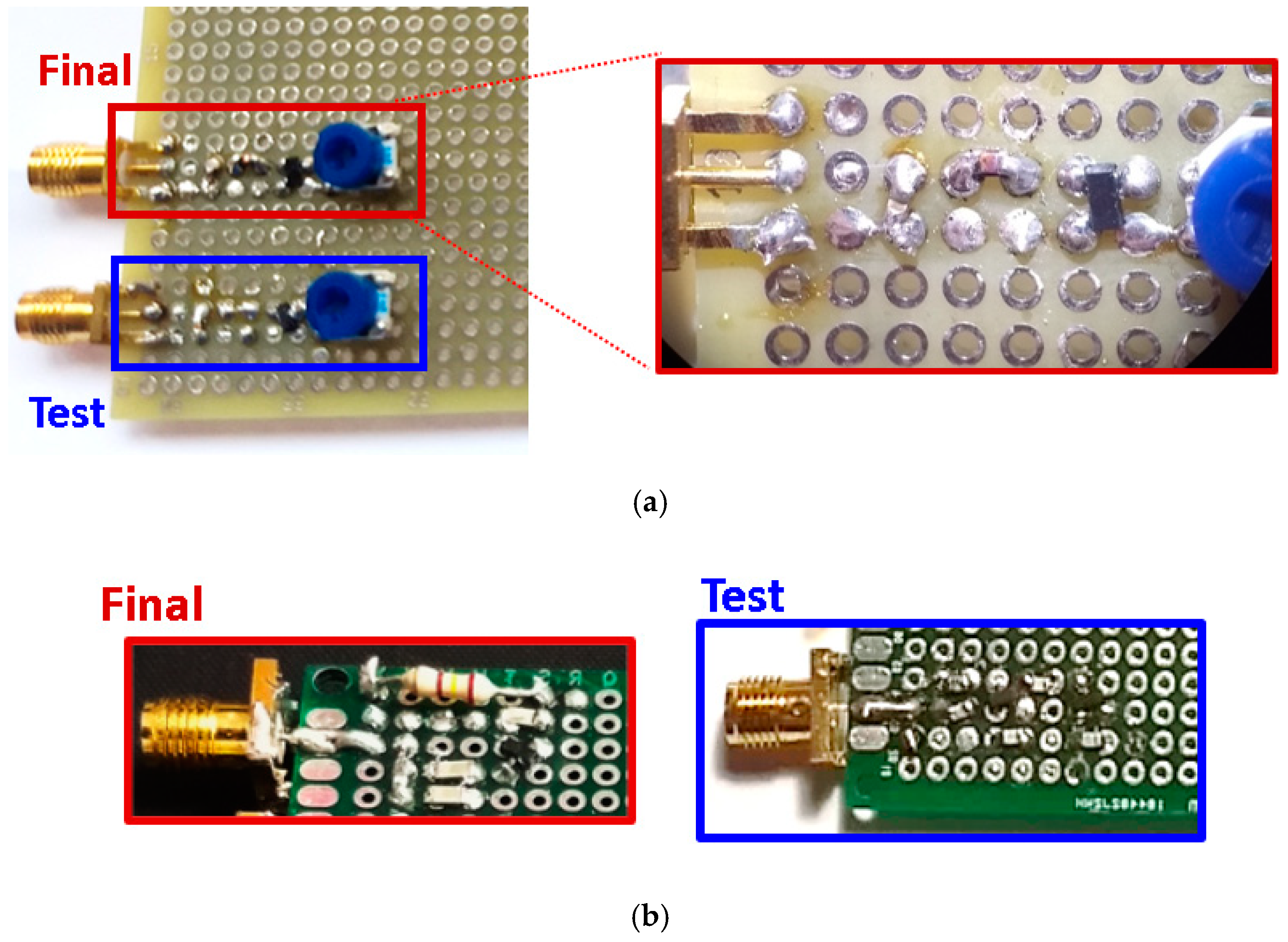
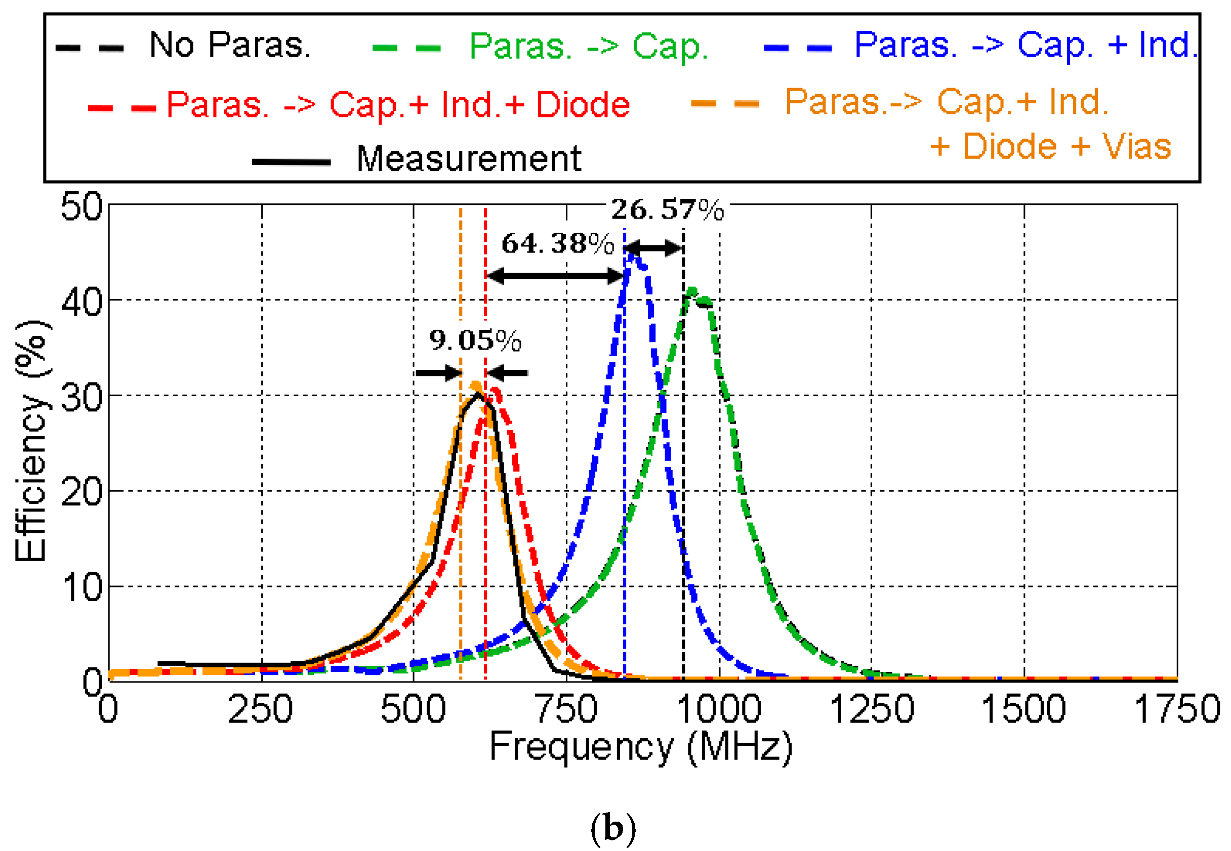
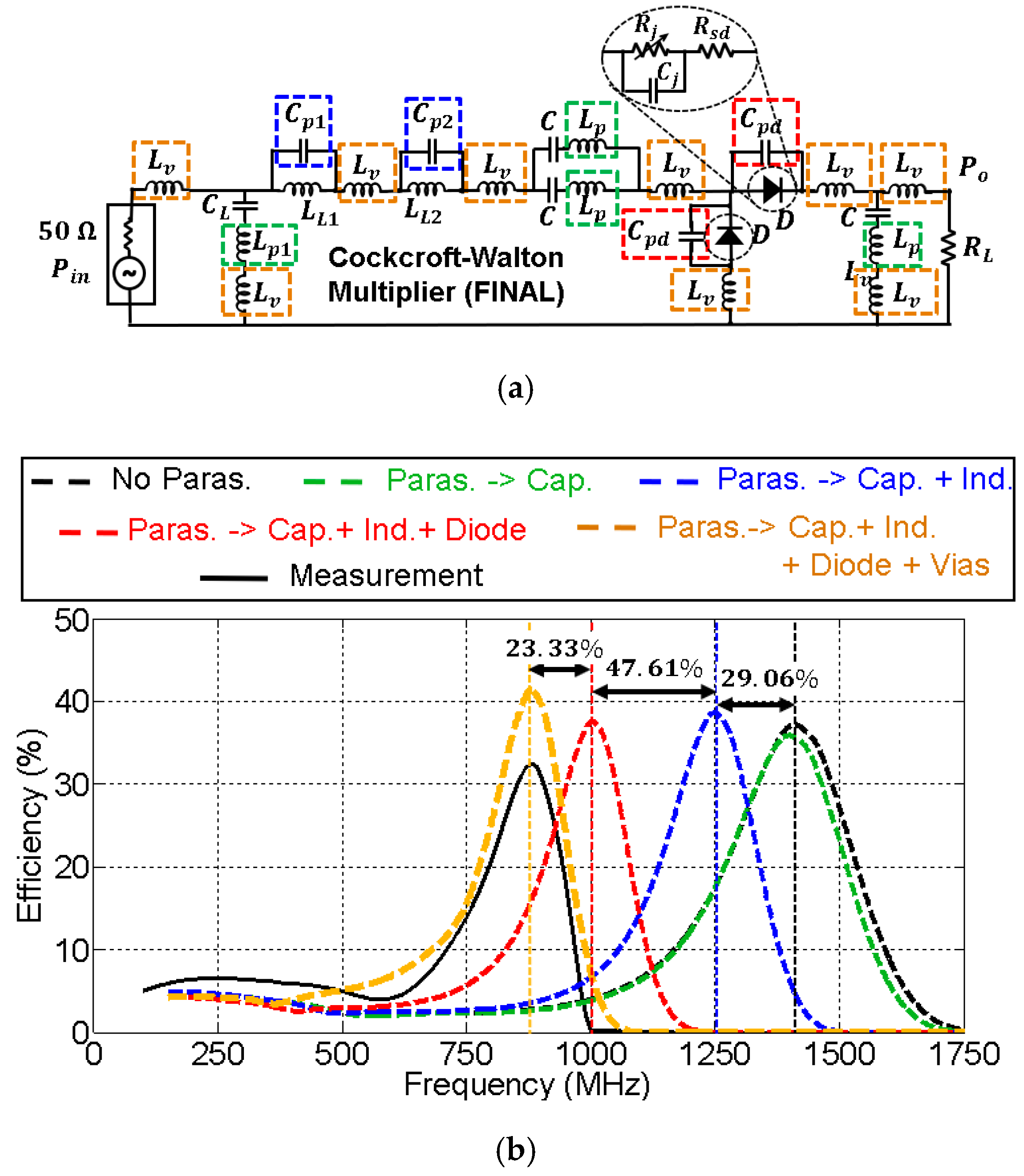
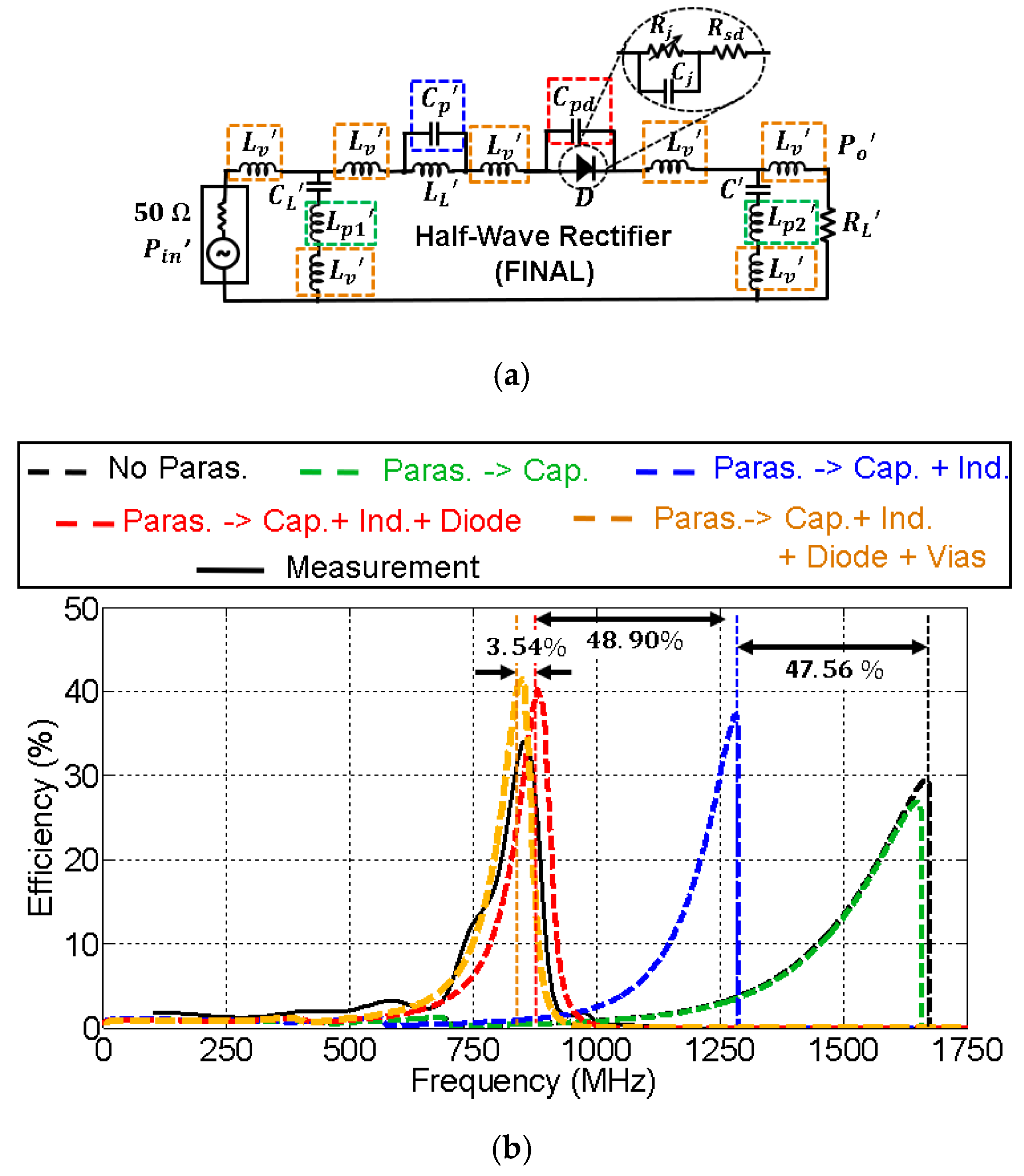
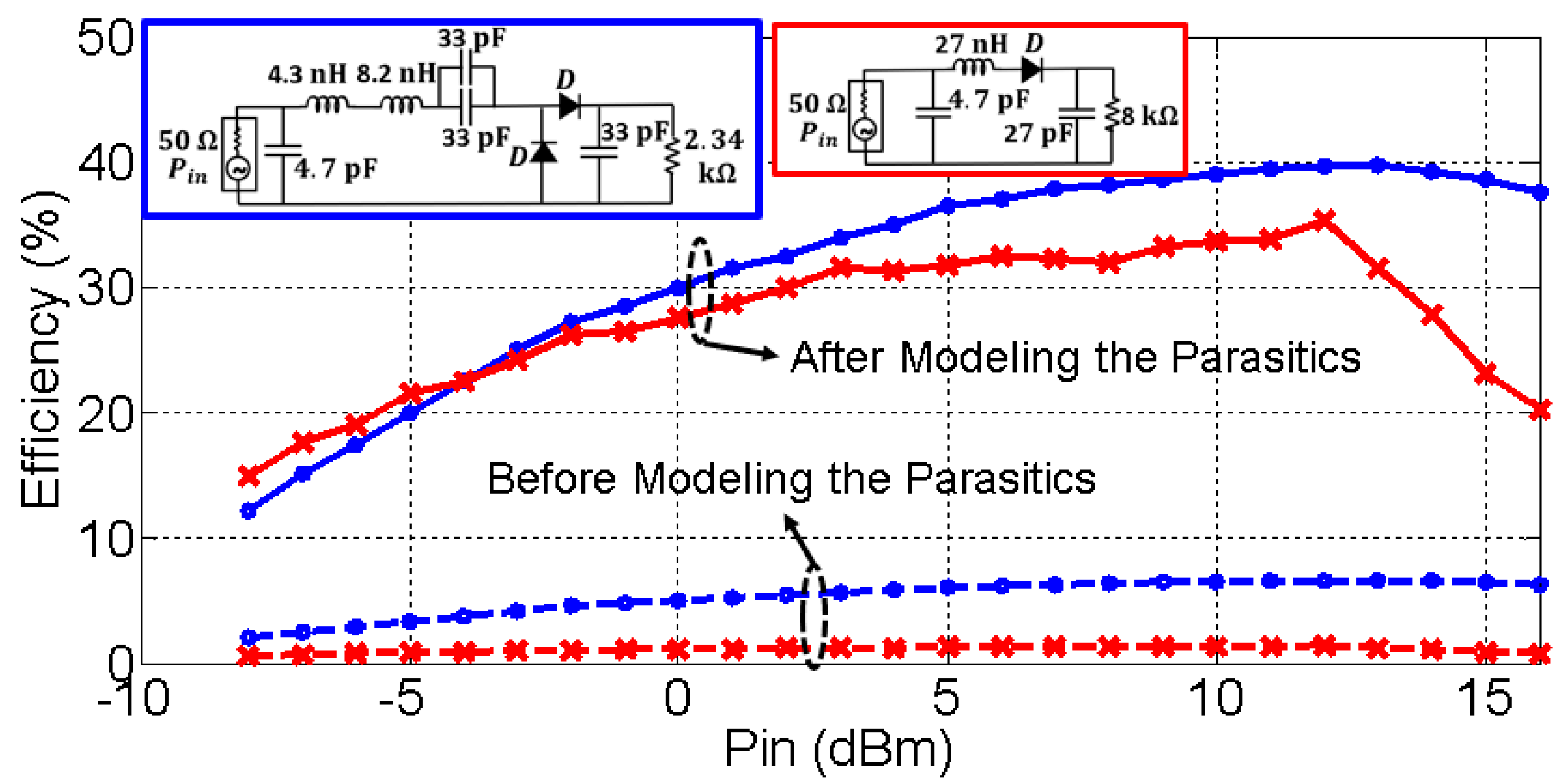
5.3. Final Circuits
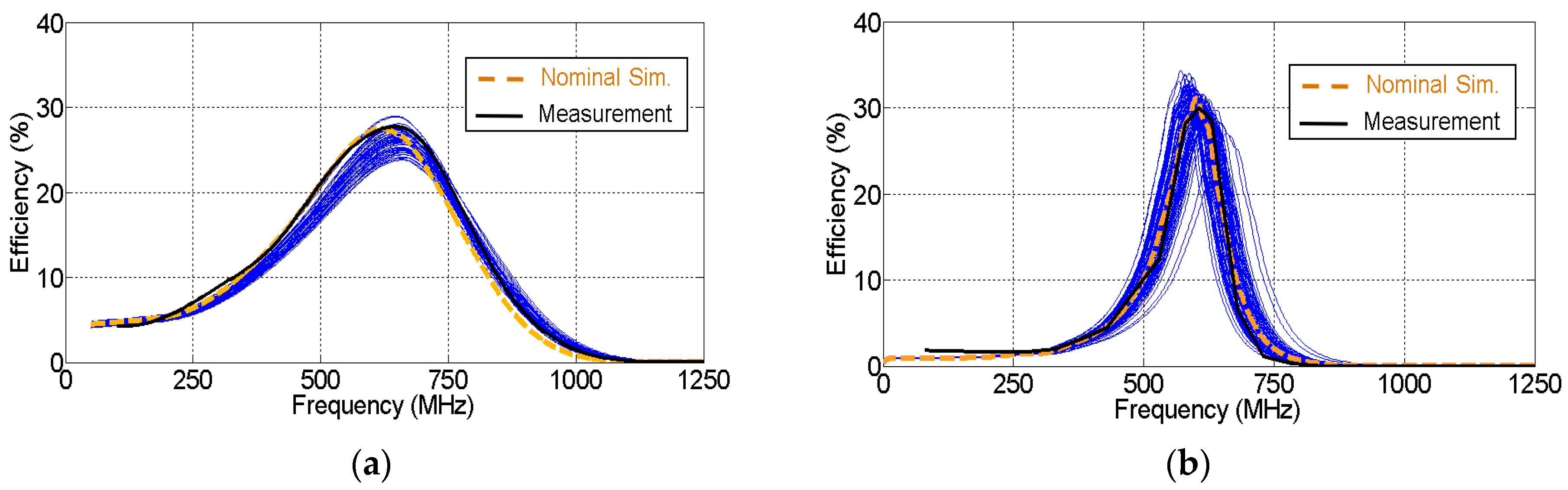
5.4. Performance Comparison of Passive Rectifiers
6. Conclusions
- The most harmful parasitics come from the components and not from the PCB. Therefore, if carefully chosen, cheaper PCBs can be utilized in order to reduce costs.
- Although the diode was known to be the limiting component in terms of losses, this work has demonstrated that it also causes a large deviation with respect to the expected frequency response. Actually, it has the most harmful parasitic element, contributing two-thirds of the total frequency displacements in both Cockcroft–Walton and half–wave circuits. In that sense, future MoS2 diodes could potentially help to improve the efficiency of rectifier circuits, since their parasitics are shown to be very low [24] compared to traditional Schottky diodes.
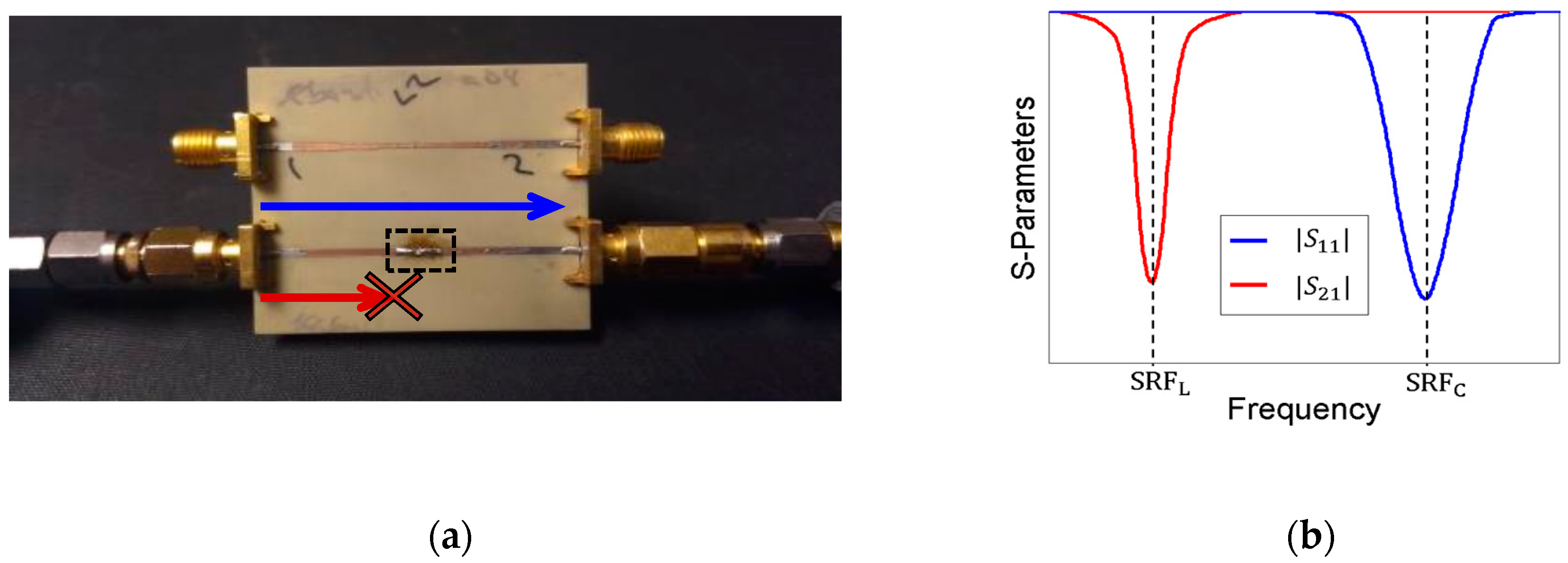
- The parasitic inductance associated with the capacitors is completely negligible. This fact allows one to use cheaper capacitors and reduce costs. It also allows one to use higher values of the capacitor in the rectifier stage, in order to reduce the DC output ripple when feeding the sensor. Note that the choice of this capacitor is a trade-off between the output ripple of the circuit, and its self-resonant frequency (SRF). The higher the value of the capacitor is, the lower the output ripple and the higher the parasitics. However, they do not affect the behavior of the circuit.
Author Contributions
Funding
Conflicts of Interest
References
- Luo, Y.; Pu, L.; Wang, G.; Zhao, Y. RF Energy Harvesting Wireless Communications: RF Environment, Device Hardware and Practical Issues. Sensors 2019, 19, 3010. [Google Scholar] [CrossRef] [PubMed]
- Partal, H.P.; Belen, M.A.; Partal, S.Z. Design and realization of an ultra-low power sensing RF energy harvesting module with its RF and DC sub-components. Int. J. RF Microw. Comput. Aided Eng. 2019, 29, 21622. [Google Scholar] [CrossRef]
- Bouchouicha, D.; Dupont, F.; Latrach, M.; Ventura, L. Ambient RF Energy Harvesting. In Proceedings of the International Conference on Renewable Energies and Power Quality (ICREPQ’10), Granada, Spain, 23–25 March 2010. [Google Scholar]
- Alex-Amor, A.; Padilla, P.; Fernández-González, J.M.; Sierra-Castañer, M. A miniaturized ultrawideband Archimedean spiral antenna for low-power sensor applications in energy harvesting. Microw. Opt. Technol. Lett. 2018, 61, 211–216. [Google Scholar] [CrossRef]
- Alex-Amor, A.; Palomares-Caballero, Á.; Fernández-González, J.M.; Padilla, P.; Marcos, D.; Sierra-Castañer, M.; Esteban, J. RF Energy Harvesting System Based on an Archimedean Spiral Antenna for Low-Power Sensor Applications. Sensors 2019, 19, 1318. [Google Scholar] [CrossRef]
- Rinne, J.; Keskinen, J.; Berger, P.R.; Lupo, D.; Valkama, M. M2M Communication Assessment in Energy-Harvesting and Wake-Up Radio Assisted Scenarios Using Practical Components. Sensors 2018, 18, 3992. [Google Scholar] [CrossRef]
- Ehiagwina, F.O.; Kehinde, O.O.; Iromin, N.A.; Nafiu, A.S.; Punetha, D. Ultra-Low Power Wireless Sensor Networks: Overview of Applications, Design Requirements and Challenges. ABUAD J. Eng. Res. Dev. 2018, 1, 331–345. [Google Scholar]
- Jawad, H.M.; Nordin, R.; Gharghan, S.K.; Jawad, A.M.; Ismail, M. Energy-Efficient Wireless Sensor Networks for Precision Agriculture: A Review. Sensors 2017, 17, 1781. [Google Scholar] [CrossRef]
- Lloret, J.; Garcia, M.; Bri, D.; Sendra, S. A Wireless Sensor Network Deployment for Rural and Forest Fire Detection and Verification. Sensors 2009, 9, 8722–8747. [Google Scholar] [CrossRef]
- Hagerty, J.A.; Helmbrecht, F.B.; McCalpin, W.H.; Zane, R.; Popovic, Z.B. Recycling Ambient Microwave Energy with Broad-Band Rectenna Arrays. IEEE Trans. Microw. Theory Tech. 2004, 52, 1014–1024. [Google Scholar] [CrossRef]
- Hande, A.; Bridgelall, R.; Zoghi, B. Vibration Energy Harvesting for Disaster Asset Monitoring Using Active RFID Tags. Proc. IEEE 2010, 98, 1620–1628. [Google Scholar] [CrossRef]
- Mishra, D.; De, S.; Jana, S.; Basagni, S.; Chowdhury, K.; Heinzelman, W. Smart RF energy harvesting communications: challenges and opportunities. IEEE Commun. Mag. 2015, 53, 70–78. [Google Scholar] [CrossRef]
- Zeng, Z.; Estrada-López, J.J.; Abouzied, M.A.; Sánchez-Sinencio, E. A Reconfigurable rectifier with optimal loading point determination for RF Energy Harvesting from −22 dBm to −2 dBm. IEEE Trans. Circuits Syst. II 2019. [Google Scholar] [CrossRef]
- Soyata, T.; Copeland, L.; Heinzelman, W. RF Energy Harvesting for Embedded Systems: A Survey of Tradeoffs and Methodology. IEEE Circuits Syst. Mag. 2016, 16, 22–57. [Google Scholar] [CrossRef]
- Moghaddam, A.K.; Chuah, J.H.; Harikrishnan, R.; Jalil, A.; Mak, P.I.; Martins, R.P. A 73.9%-Efficiency CMOS Rectifier Using a Lower DC Feeding (LDCF) Self-Body-Biasing Technique for Far-Field RF Energy-Harvesting Systems. IEEE Trans. Circuits Syst. I Reg. Pap. 2017, 64, 992–1002. [Google Scholar] [CrossRef]
- Bolt, R.; Magno, M.; Burger, T.; Romani, A.; Benini, L. Kinetic AC/DC Converter for Electromagnetic Energy Harvesting in Autonomous Wearable Devices. IEEE Trans. Circuits Syst. II Exp. Briefs 2017, 64, 1422–1426. [Google Scholar] [CrossRef]
- Escobedo, P.; Pérez de Vargas-Sansalvador, I.M.; Carvajal, M.; Capitán-Vallvey, L.F.; Palma, A.J.; Martínez-Olmos, A. Flexible passive tag based on light energy harvesting for gas threshold determination in sealed environments. Sens. Actuators B Chem. 2016, 236, 226–232. [Google Scholar] [CrossRef]
- Erkmen, F.; Almoneef, T.S.; Ramahi, O.M. Electromagnetic Energy Harvesting Using Full-Wave Rectification. IEEE Trans. Microw. Theory Tech. 2017, 65, 1843–1851. [Google Scholar] [CrossRef]
- HSMS-2820 and HSMS-2850 Datasheets; BroadCom Inc.: San José, CA, USA; Available online: http://www.broadcom.com (accessed on 27 October 2019).
- Georgiadis, A.; Vera Andia, G.; Collado, A. Rectenna design and optimization using reciprocity theory and harmonic balance analysis for electromagnetic (EM) energy harvesting. IEEE Antennas Wirel. Propag. Lett. 2010, 9, 444–446. [Google Scholar] [CrossRef]
- Pozar, D.M. Microwave Engineering, 3rd ed.; Wiley: Hoboken, NJ, USA, 2005. [Google Scholar]
- Johnson, H.W.; Graham, M. High-Speed Digital Design: A Handbook of Black Magic; Prentice Hall Inc.: Upper Saddle River, NJ, USA, 1993; p. 259. [Google Scholar]
- Gao, Q.; Zhang, Z.; Xu, X.; Song, J.; Li, X.; Wu, Y. Scalable high performance radio frequency electronics based on large domain bilayer MoS2. Nat. Commun. 2018, 9, 4778. [Google Scholar] [CrossRef]
- Zhang, X.; Grajal, J.; Vazquez-Roy, J.L.; Radhakrishna, U.; Wang, X.; Chern, W.; Zhou, L.; Lin, Y.; Shen, P.-C.; Ji, X.; et al. Two-dimensional MoS2-enabled flexible rectenna for Wi-Fi-band wireless energy harvesting. Nature 2019, 566, 368–372. [Google Scholar] [CrossRef]
- Masuch, J.; Delgado-Restituto, M.; Milosevic, D.; Baltus, P. An RF-to-DC Energy Harvester for co-Integration in a Low-Power 2.4 GHz Transceiver Frontend. In Proceedings of the 2012 IEEE International Symposium on Circuits and Systems (ISCAS) 2012, Seoul, Korea, 20–23 May 2012; pp. 680–683. [Google Scholar]
- Umeda, T.; Yoshida, H.; Sekine, S.; Fujita, Y.; Suzuki, T.; Otaka, S. A 950-MHz rectifier circuit for sensor network tags with 10-m distance. IEEE J. Solid-State Circuits 2006, 41, 35–41. [Google Scholar] [CrossRef]
- Nintanavongsa, P.; Muncuk, U.; Lewis, D.R.; Chowdhury, K.R. Design optimization and implementation for RF energy harvesting circuits. IEEE J. Emerg. Sel. Top. Circuits Syst. 2012, 2, 24–33. [Google Scholar] [CrossRef]
- Chaour, I.; Fakhfakh, A.; Kanoun, O. Enhanced passive RF-DC converter circuit efficiency for low RF energy harvesting. Sensors 2017, 17, 546. [Google Scholar] [CrossRef] [PubMed]
- Song, C.; Huang, Y.; Zhou, J.; Carter, P. Improved Ultrawideband Rectennas Using Hybrid Resistance Compression Technique. IEEE Trans. Antennas Propag. 2017, 65, 2057–2062. [Google Scholar] [CrossRef]
- Riviere, J.; Douyere, A.; Oree, S.; Lan Sun Luk, J.-D. A 2.45 GHz ISM Band CPW Rectenna for Low Power Levels. Prog. Electromagn. Res. C 2017, 77, 101–110. [Google Scholar] [CrossRef]
- Mattsson, M.; Kolitsidas, C.I.; Jonsson, B.L.G. Dual-Band Dual Polarized Full-Wave Rectenna Based on Differential Field Sampling. IEEE Antennas Wirel. Propag. Lett. 2018, 17, 956–959. [Google Scholar] [CrossRef]


| Model | Value | SRF (GHz) | Parasitic |
|---|---|---|---|
| 4,841,372 (Fair-Rite) | 33 nH | 1.50 | 0.34 pF |
| 106–909 (Murata) | 8.2 nH | 4.00 | 0.19 pF |
| 795–8290 (TDK) | 4.3 nH | 7.64 | 0.10 pF |
| 464–6773 (AVX) | 33 pF | 2.20 | 0.16 nH |
| 532–2945 (TE Connect.) | 47 nH | 1.96 | 0.14 pF |
| CW160,808 (Bourns) | 27 nH | 2.10 | 0.21 pF |
| 2,310,325 (Multicomp) | 2.7 pF | 4.97 | 0.38 nH |
| ATC 500S (ATC) | 4.7 pF | 8.32 | 0.078nH |
| 2,809,454 (Kemet) | 27 pF | 4.84 | 0.040 nH |
© 2019 by the authors. Licensee MDPI, Basel, Switzerland. This article is an open access article distributed under the terms and conditions of the Creative Commons Attribution (CC BY) license (http://creativecommons.org/licenses/by/4.0/).
Share and Cite
Alex-Amor, A.; Moreno-Núñez, J.; Fernández-González, J.M.; Padilla, P.; Esteban, J. Parasitics Impact on the Performance of Rectifier Circuits in Sensing RF Energy Harvesting. Sensors 2019, 19, 4939. https://doi.org/10.3390/s19224939
Alex-Amor A, Moreno-Núñez J, Fernández-González JM, Padilla P, Esteban J. Parasitics Impact on the Performance of Rectifier Circuits in Sensing RF Energy Harvesting. Sensors. 2019; 19(22):4939. https://doi.org/10.3390/s19224939
Chicago/Turabian StyleAlex-Amor, Antonio, Javier Moreno-Núñez, José M. Fernández-González, Pablo Padilla, and Jaime Esteban. 2019. "Parasitics Impact on the Performance of Rectifier Circuits in Sensing RF Energy Harvesting" Sensors 19, no. 22: 4939. https://doi.org/10.3390/s19224939
APA StyleAlex-Amor, A., Moreno-Núñez, J., Fernández-González, J. M., Padilla, P., & Esteban, J. (2019). Parasitics Impact on the Performance of Rectifier Circuits in Sensing RF Energy Harvesting. Sensors, 19(22), 4939. https://doi.org/10.3390/s19224939