Nanomechanical Characterization of Vertical Nanopillars Using an MEMS-SPM Nano-Bending Testing Platform

 ,
,  ,
,
Abstract
:1. Introduction
2. Development of a MEMS Scanning Probe Microscope
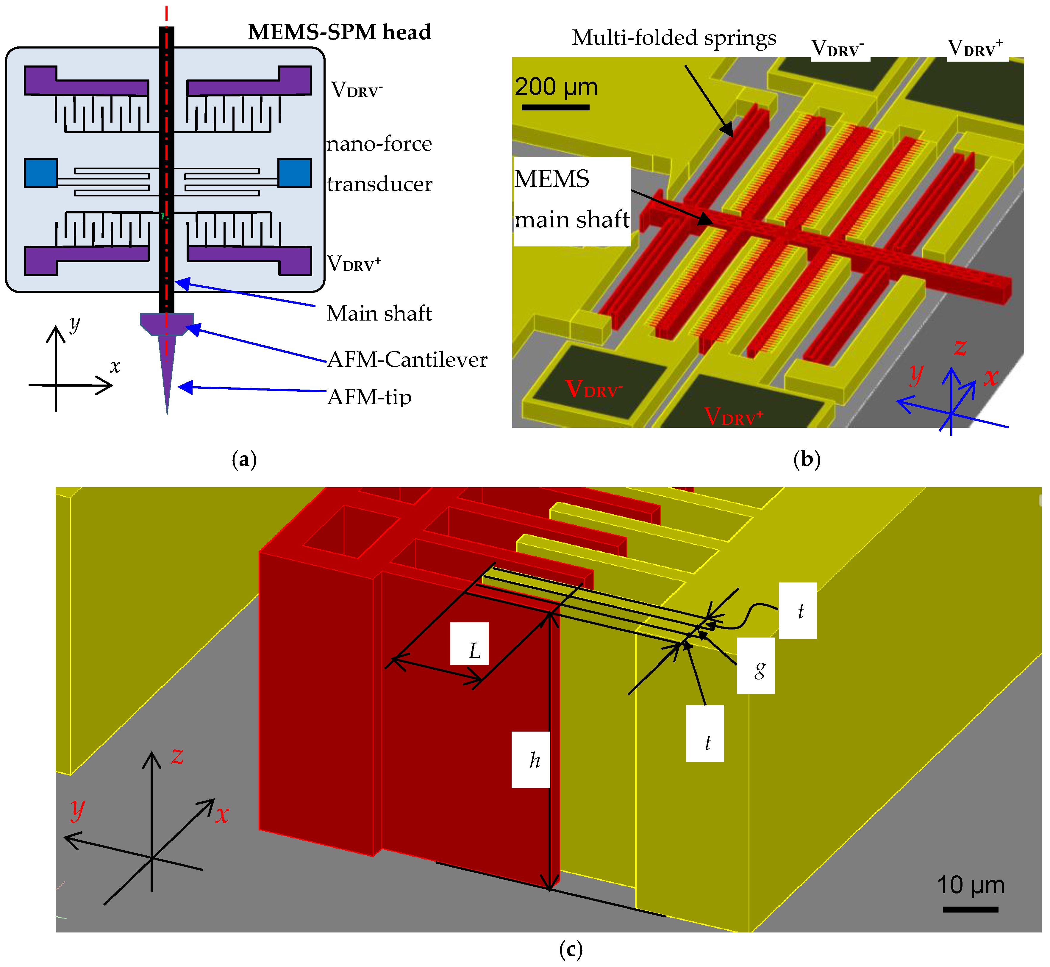
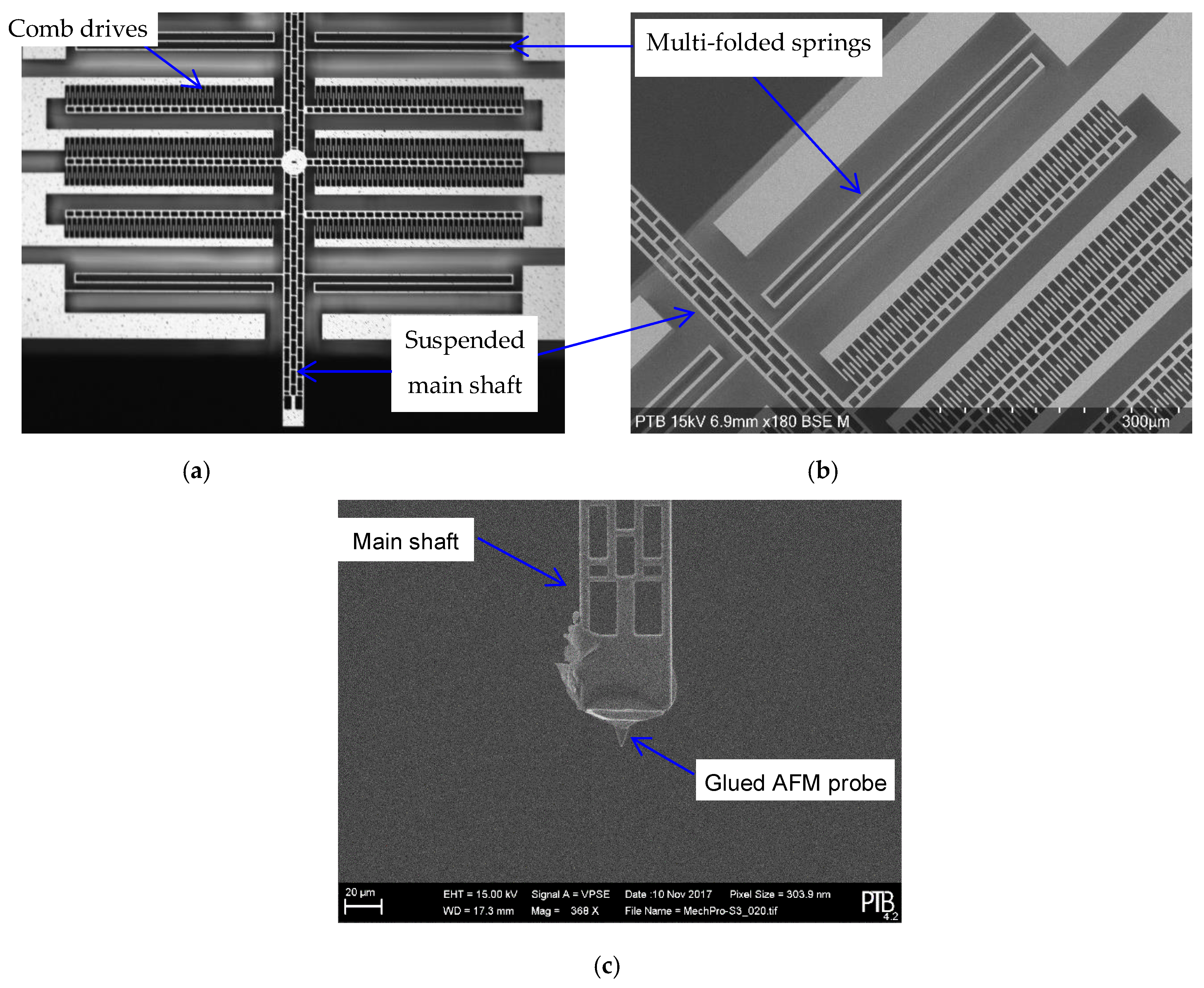
2.1. MEMS-SPM Head
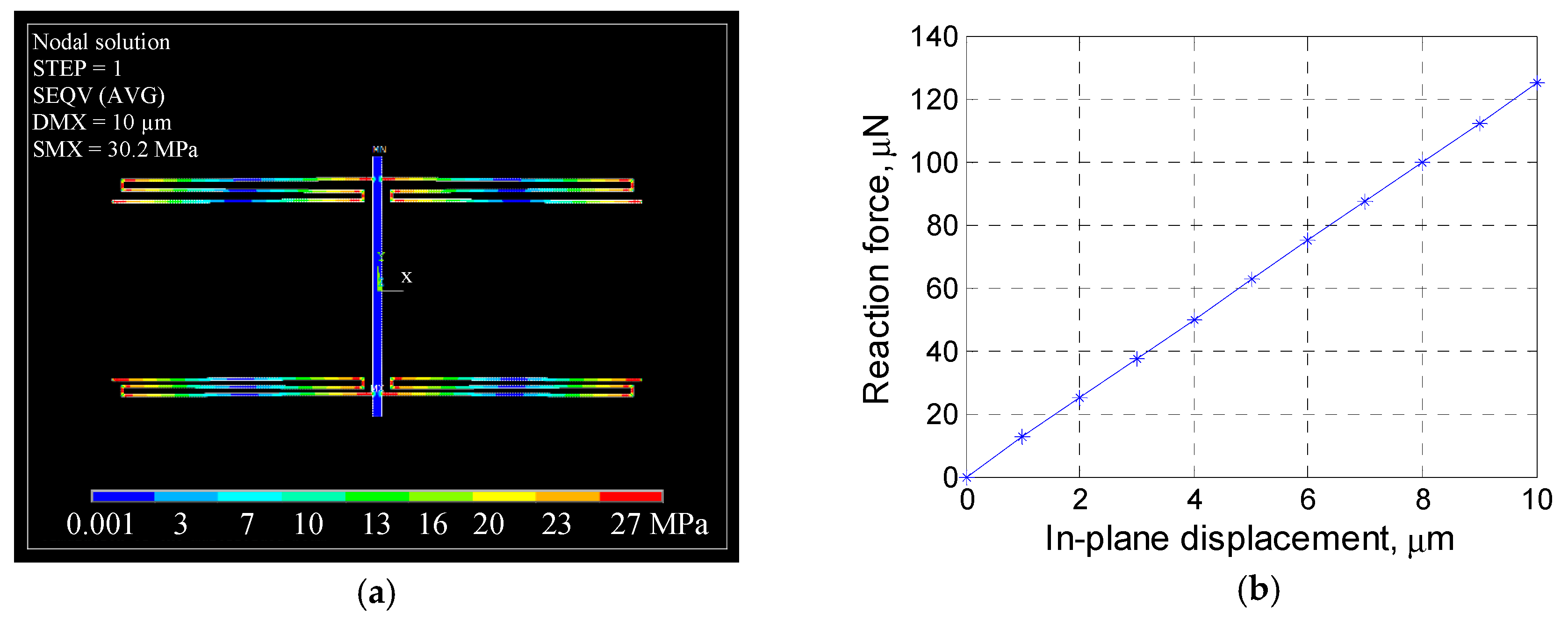
2.2. Prototyping
3. Nanomechanical Characterization of Nanopillars Using the MEMS-SPM
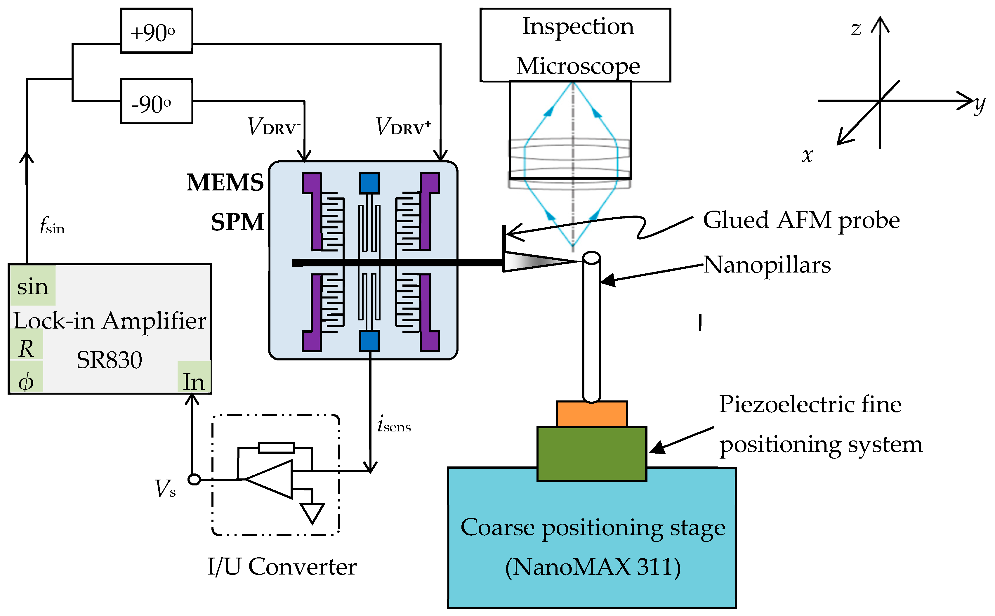
3.1. System Configuration
3.2. Sample Preparation
3.3. First Results
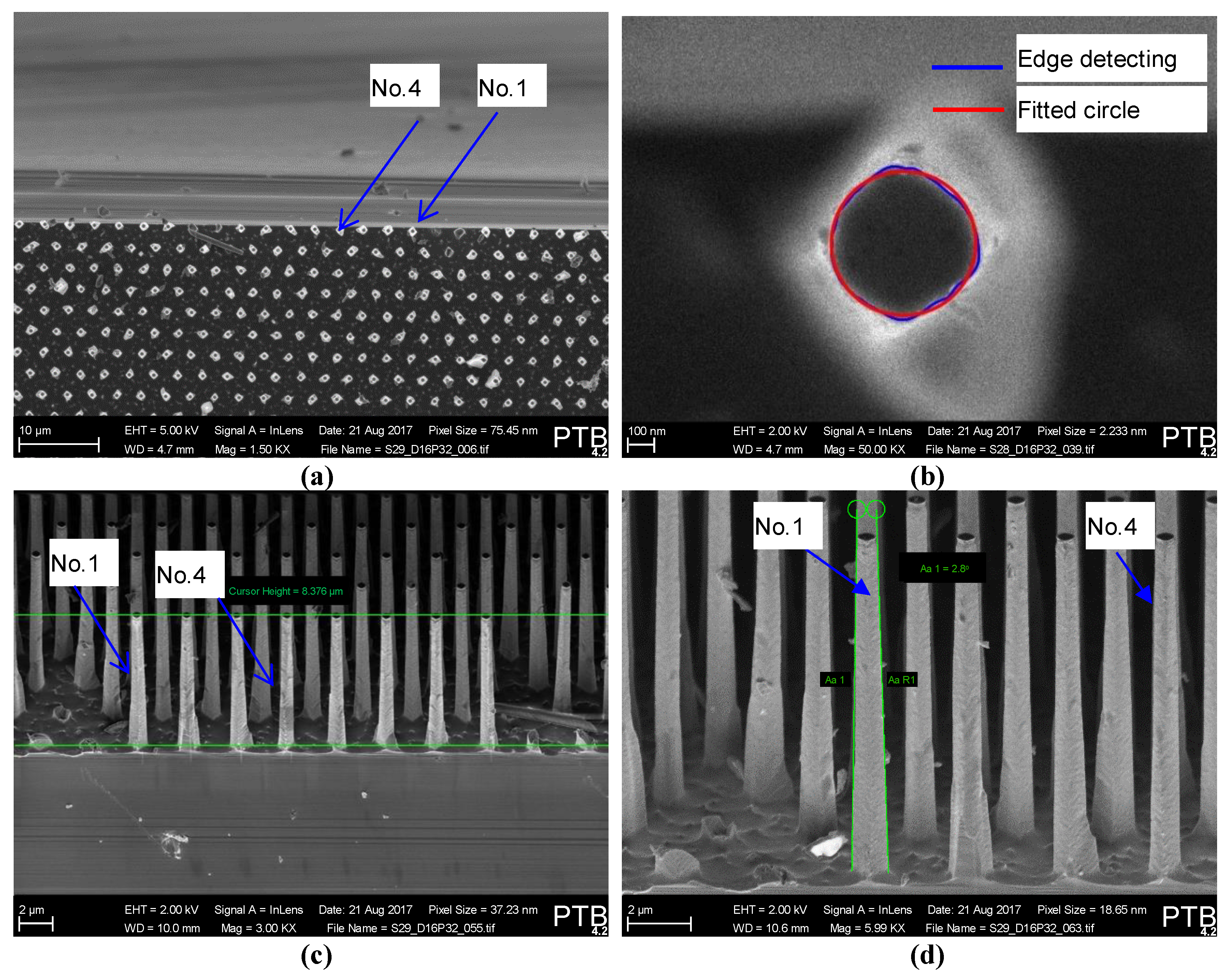
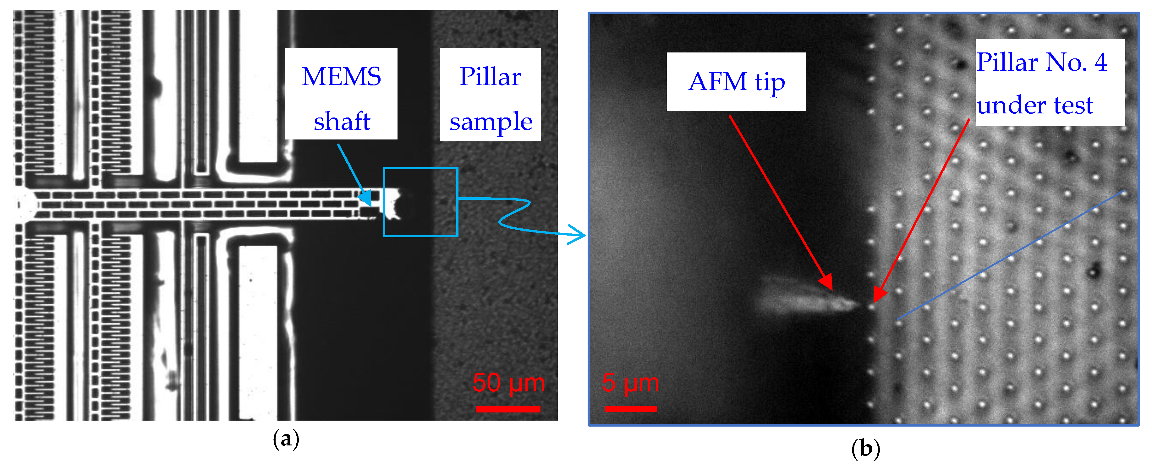
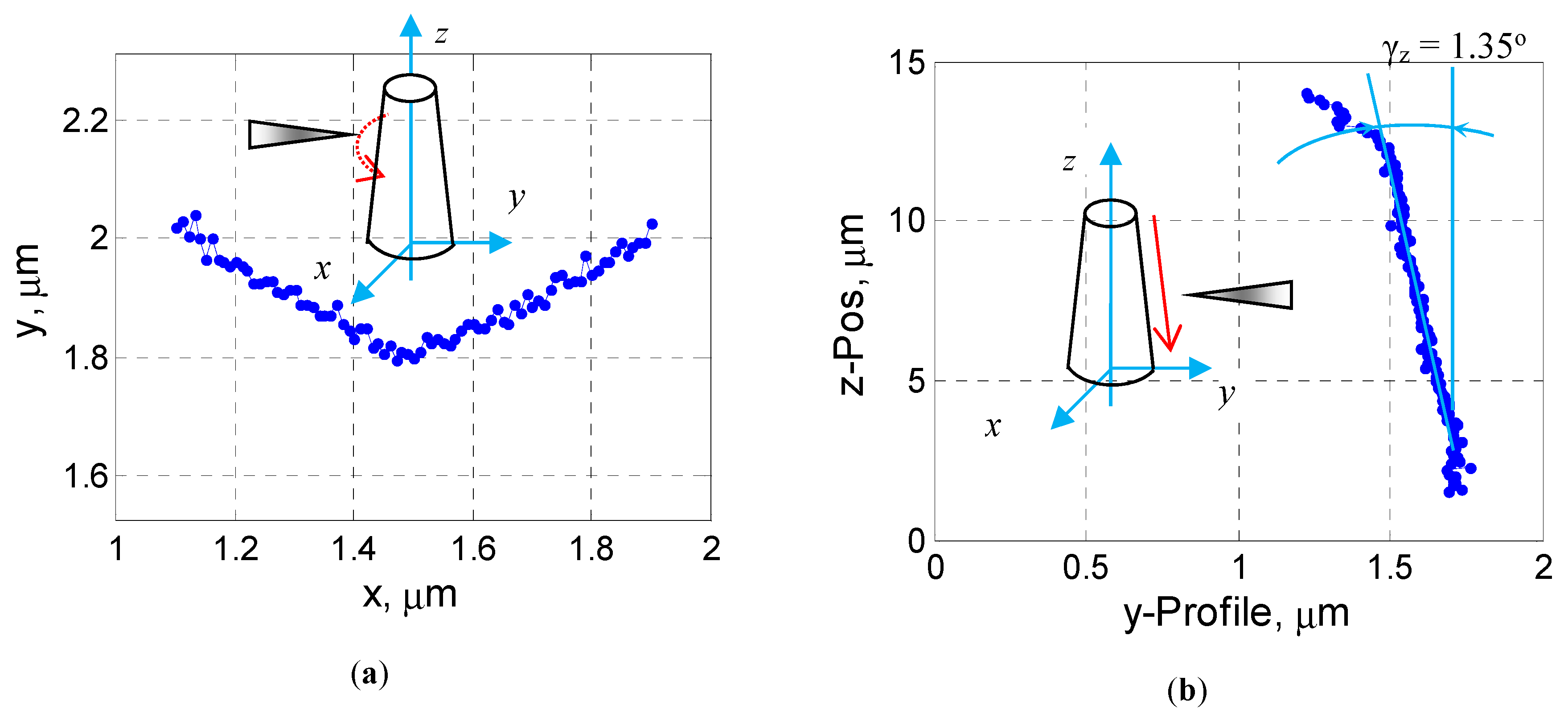
3.3.1. Surface Profiling of Nanopillars
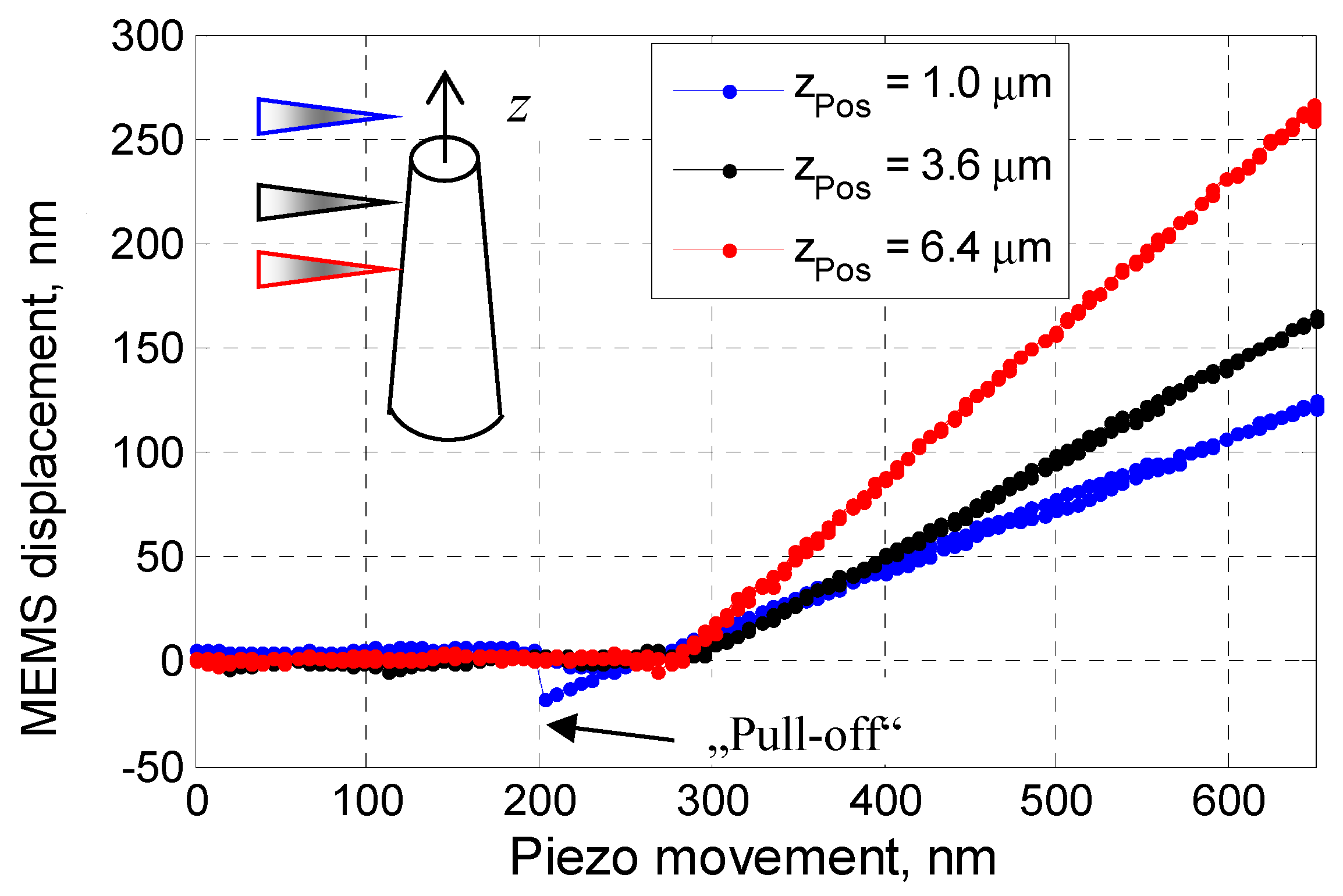
3.3.2. Nano-Bending Testing
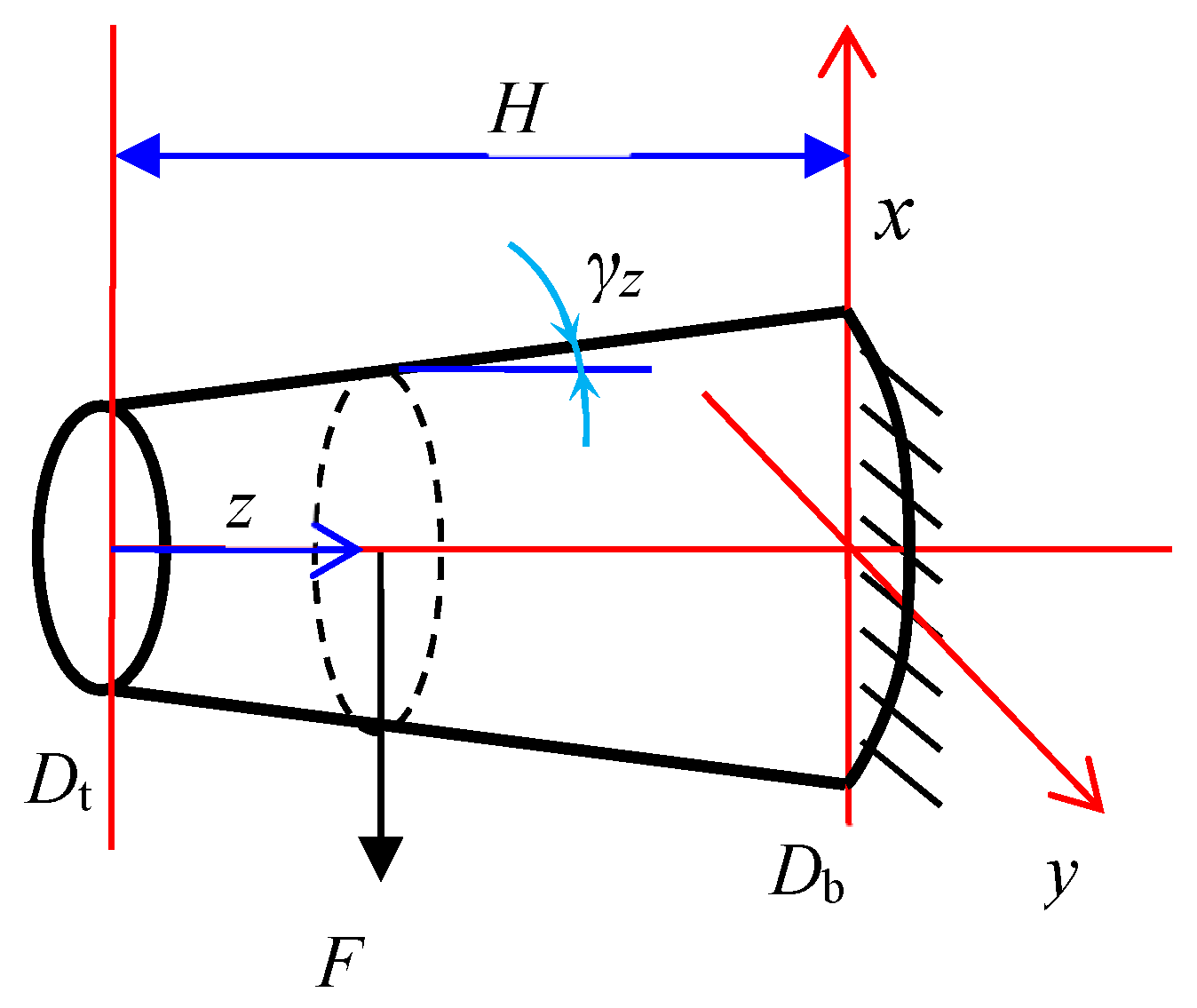
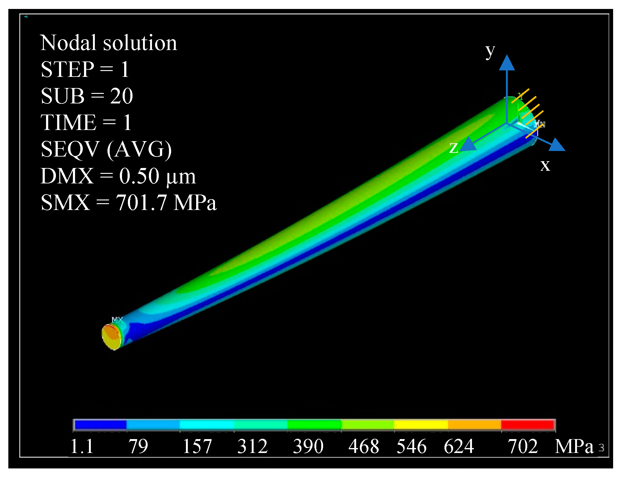
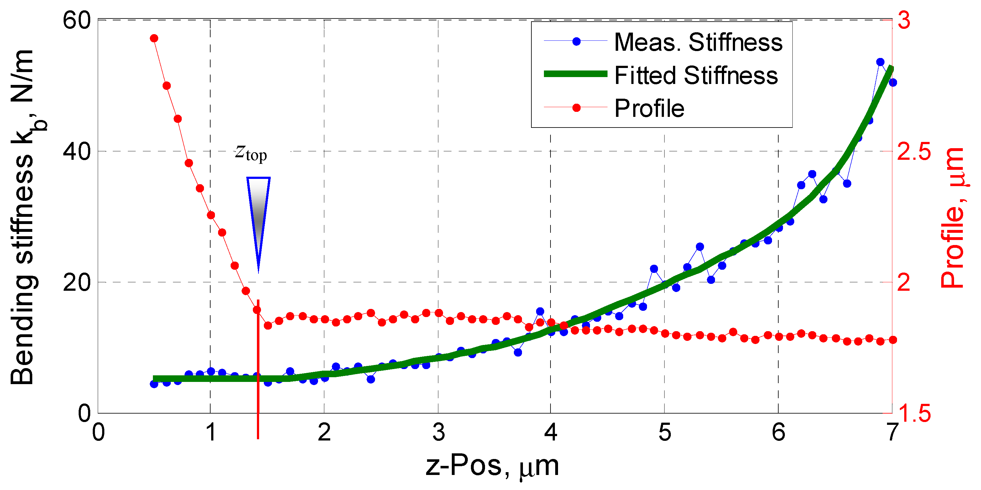
3.3.3. Measurement Data Evaluation for Tapered Nanopillars
3.3.4. Measurement Uncertainty Estimation and Discussion
4. Summary and Outlook
Author Contributions
Funding
Conflicts of Interest
References
- Lee, D.Y.; Kim, H.; Li, H.M.; Jang, A.R.; Lim, Y.D.; Cha, S.N.; Park, Y.J.; Kang, D.J.; Yoo, W.J. Hybrid energy harvester based on nanopillar solar cells and PVDF nanogenerator. Nanotechnology 2013, 24, 175402. [Google Scholar] [CrossRef] [PubMed]
- Sun, Y.M.; Liu, N.; Cui, Y. Promises and challenges of nanomaterials for lithium-based rechargeable batteries. Nat. Energy 2016, 1, 16071. [Google Scholar] [CrossRef]
- Yu, F.; Yao, S.; Römer, F.; Witzigmann, B.; Schimpke, T.; Strassburg, M.; Bakin, A.; Schumacher, H.W.; Peiner, E.; Wasisto, H.S.; et al. GaN nanowire arrays with nonpolar sidewalls for vertically integrated field-effect transistors. Nanotechnology 2017, 28, 095206. [Google Scholar] [CrossRef] [PubMed]
- Wasisto, H.S.; Merzsch, S.; Stranz, A.; Waag, A.; Uhde, E.; Salthammer, T.; Peiner, E. Silicon Nanowire Resonators—Aerosol nanoparticle mass sensing in the workplace. IEEE Nanotechnol. Mag. 2013, 7, 18–23. [Google Scholar] [CrossRef]
- Kou, J.Z.; Zhang, Y.; Liu, Y.; Zhang, K.; Liu, W.; Zhai, J.Y. Nano-force sensor based on a single tellurium microwire. Semicond. Sci. Technol. 2017, 32, 074001. [Google Scholar] [CrossRef]
- Shiu, J.Y.; Aires, L.; Lin, Z.; Vogel, V. Nanopillar force measurements reveal actin-cap-mediated YAP mechanotransduction. Nat. Cell Biol. 2018, 20, 262–271. [Google Scholar] [CrossRef] [PubMed]
- Antonov, P.V.; Zuiddam, M.R.; Frenken, J.W.M. Fabrication of high-aspect ratio silicon nanopillars for tribological experiments. J. Micro/Nanolithogr. MEMS MOEMS 2015, 14, 044506. [Google Scholar] [CrossRef]
- Wang, S.L.; Shan, Z.W.; Huang, H. The Mechanical Properties of Nanowires. Adv. Sci. 2017, 4, 1600332. [Google Scholar]
- Qi, H.J.; Teo, K.B.K.; Lau, K.K.S.; Boyce, M.C.; Milne, W.I.; Robertson, J.; Gleason, K.K. Determination of mechanical properties of carbon nanotubes and vertically aligned carbon nanotube forests using nanoindentation. J. Mech. Phys. Solids 2003, 51, 2213–2237. [Google Scholar] [CrossRef]
- Jarzabek, D.M.; Kaufmann, A.N.; Schift, H.; Rymuza, Z.; Jung, T.A. Elastic modulus and fracture strength evaluation on the nanoscale by scanning force microscope experiments. Nanotechnology 2014, 25, 215701. [Google Scholar] [CrossRef] [PubMed]
- Wang, Z.L.; Song, J. Piezoelectric nanogenerators based on zinc oxide nanowire arrays. Science 2006, 312, 242–246. [Google Scholar] [CrossRef] [PubMed]
- Gao, S.; Zhang, Z.; Wu, Y.; Herrmann, K. Towards quantitative determination of the spring constant of a scanning force microscope cantilever with a microelectromechanical nano-force actuator. Meas. Sci. Technol. 2010, 21, 015103. [Google Scholar] [CrossRef]
- Wagner, R.; Moon, R.; Pratt, J.; Shaw, G.; Raman, A. Uncertainty quantification in nanomechanical measurements using the atomic force microscope. Nanotechnology 2011, 22, 455703. [Google Scholar] [CrossRef] [PubMed]
- Dziekoński, C.; Dera, W.; Jarząbek, D. Method for lateral force calibration in atomic force microscope using MEMS microforce sensor. Ultramicroscopy 2017, 182, 1–9. [Google Scholar] [CrossRef] [PubMed]
- Tang, W.C.; Lim, M.G.; Howe, R.T. Electrostatic comb drive levitation and control method. J. Microelectromech. Syst. 1992, 1, 170–178. [Google Scholar] [CrossRef]
- Brand, U.; Gao, S.; Engl, W.; Sulzbach, T.; Stahl, S.W.; Milles, L.F.; Nesterov, V.; Li, Z. Comparing AFM cantilever stiffness measured using the thermal vibration and the improved thermal vibration methods with that of an SI traceable method based on MEMS. Meas. Sci. Technol. 2017, 28, 034010. [Google Scholar] [CrossRef]
- Esfahani, M.N.; Alaca, B.E. A review on size-dependent mechanical properties of nanowires. Adv. Eng. Mater. 2019, 21, 1900192. [Google Scholar] [CrossRef]
- Hiller, K.; Kuechler, M.; Billep, D.; Schroeter, B.; Dienel, M.; Scheibner, D.; Gessner, T. Bonding and deep RIE: A powerful combination for high-aspect-ratio sensors and actuators. In Proceedings of the Volume 5715, Micromachining and Microfabrication Process Technology X, San Jose, CA, USA, 22–27 January 2005; pp. 80–91. [Google Scholar]
- Brand, U.; Gao, S.; Doering, L.; Li, Z.; Xu, M.; Buetefisch, S.; Peiner, E.; Fruehauf, J.; Hiller, K. Smart sensors and calibration standards for high precision metrology. In Proceedings of the Volume 9517, Smart Sensors, Actuators, and MEMS VII; and Cyber Physical Systems, Barcelona, Spain, 4–6 May 2015; p. 95170V. [Google Scholar]
- Hamdana, G.; Südkamp, T.; Descoins, M.; Mangelinck, D.; Caccamo, L.; Bertke, M.; Wasisto, H.S.; Bracht, H.; Peiner, E. Towards fabrication of 3D isotopically modulated vertical silicon nanowires in selective areas by nanosphere lithography. Microelectron. Eng. 2017, 179, 74–82. [Google Scholar] [CrossRef]
- McCutcheon, W.J. Deflections and stresses in circular tapered beams and poles. Civil Eng. Pract. Des. Eng. 1983, 2, 207–233. [Google Scholar]


| Dimensions | Pillar No. 1 | Pillar No. 4 |
|---|---|---|
| Top Diameter Dt, nm | 540 ± 15 | 552 ± 15 |
| Height H, µm | 11.83 ± 0.12 | |
| Taper Angle (2γz), degree | 2.4 ± 0.2 | 1.9 ± 0.2 |
| Bottom Diameter | 1130 ± 84 | 944 ± 84 |
| Bending Stiffness kbt, N/m | Pillar No. 1 | Pillar No. 4 |
|---|---|---|
| Nominal Value | 6.8 | |
| Experimental Measurements | 5.4 ± 0.2 | 5.3 ± 0.1 |
| Analytical Estimation | 9.01 | 5.37 |
| FEM Simulation | 9.07 | 5.43 |
© 2019 by the authors. Licensee MDPI, Basel, Switzerland. This article is an open access article distributed under the terms and conditions of the Creative Commons Attribution (CC BY) license (http://creativecommons.org/licenses/by/4.0/).
Share and Cite
Li, Z.; Gao, S.; Brand, U.; Hiller, K.; Hahn, S.; Hamdana, G.; Peiner, E.; Wolff, H.; Bergmann, D. Nanomechanical Characterization of Vertical Nanopillars Using an MEMS-SPM Nano-Bending Testing Platform. Sensors 2019, 19, 4529. https://doi.org/10.3390/s19204529
Li Z, Gao S, Brand U, Hiller K, Hahn S, Hamdana G, Peiner E, Wolff H, Bergmann D. Nanomechanical Characterization of Vertical Nanopillars Using an MEMS-SPM Nano-Bending Testing Platform. Sensors. 2019; 19(20):4529. https://doi.org/10.3390/s19204529
Chicago/Turabian StyleLi, Zhi, Sai Gao, Uwe Brand, Karla Hiller, Susann Hahn, Gerry Hamdana, Erwin Peiner, Helmut Wolff, and Detlef Bergmann. 2019. "Nanomechanical Characterization of Vertical Nanopillars Using an MEMS-SPM Nano-Bending Testing Platform" Sensors 19, no. 20: 4529. https://doi.org/10.3390/s19204529
APA StyleLi, Z., Gao, S., Brand, U., Hiller, K., Hahn, S., Hamdana, G., Peiner, E., Wolff, H., & Bergmann, D. (2019). Nanomechanical Characterization of Vertical Nanopillars Using an MEMS-SPM Nano-Bending Testing Platform. Sensors, 19(20), 4529. https://doi.org/10.3390/s19204529