Fringing Electric Field Sensors for Anti-Attack at System-Level Protection


Abstract
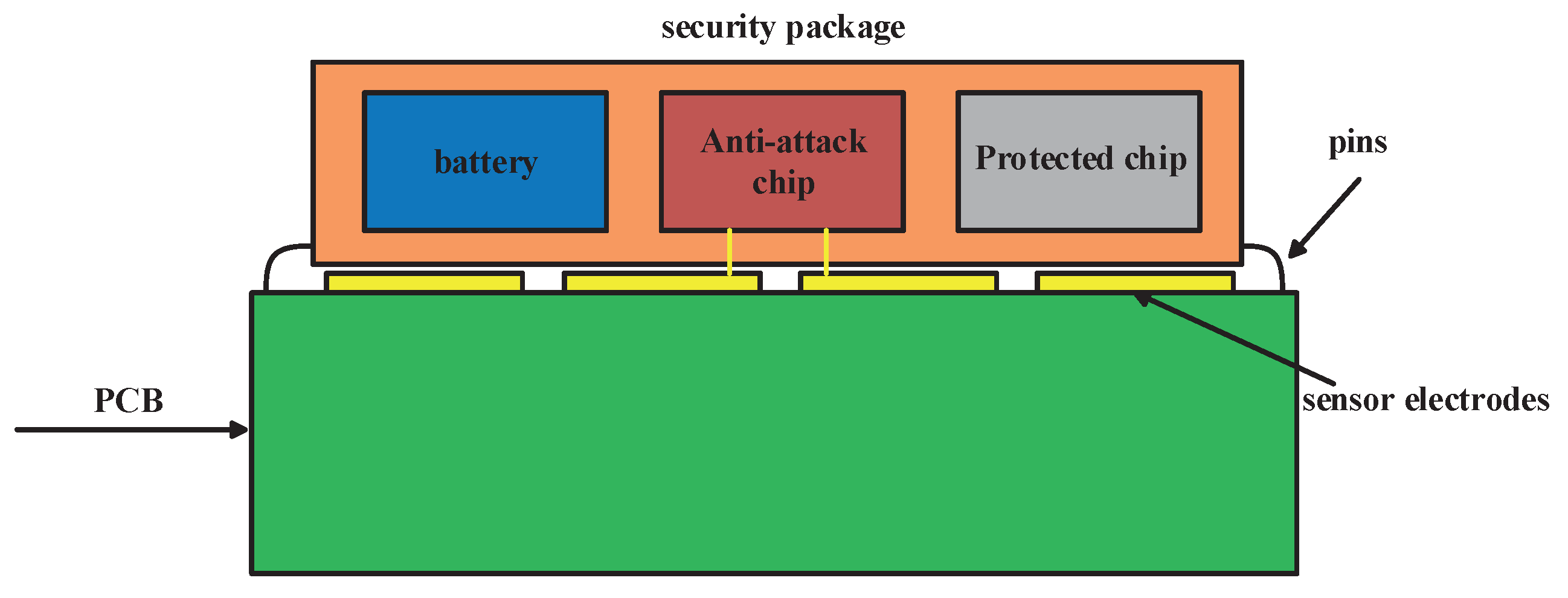
1. Introduction
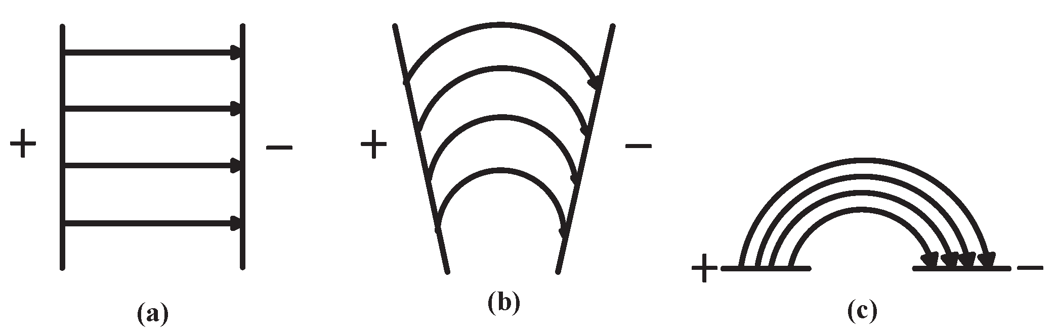
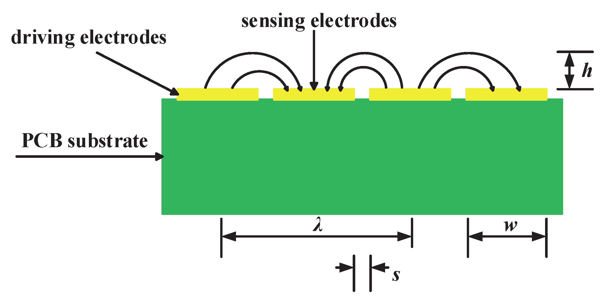
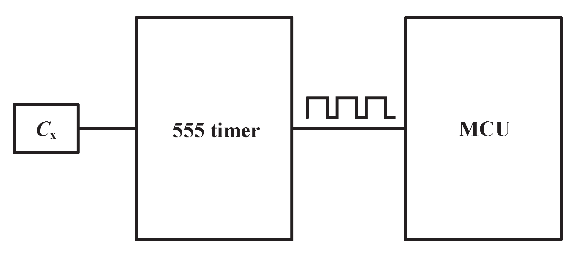
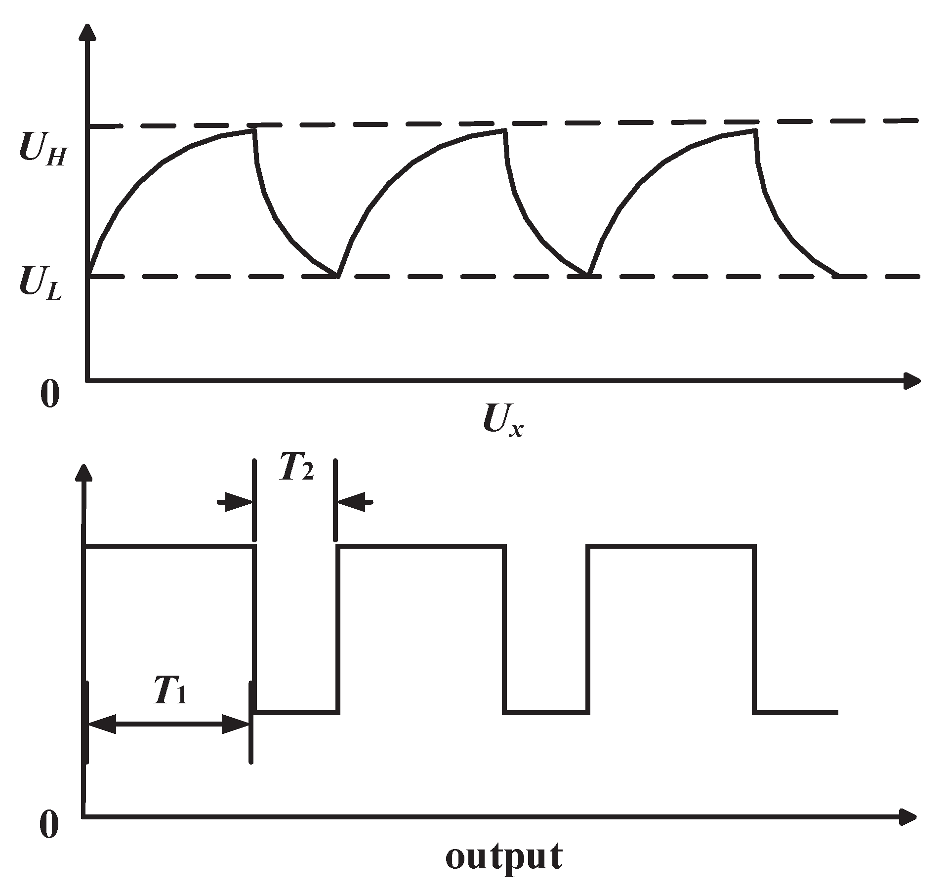
2. Theory of a Fringing Electric Field Sensor
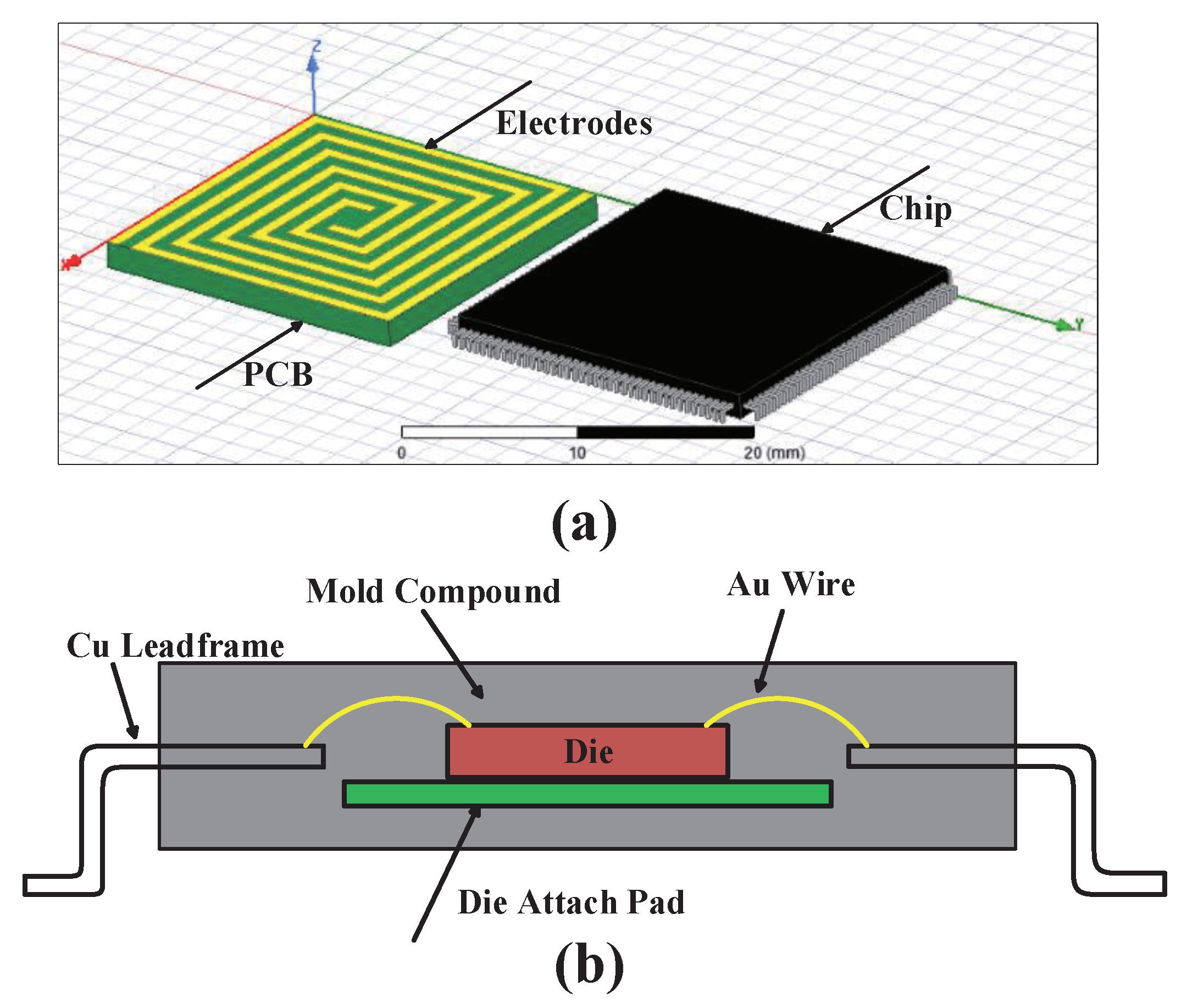
3. Design and Simulation
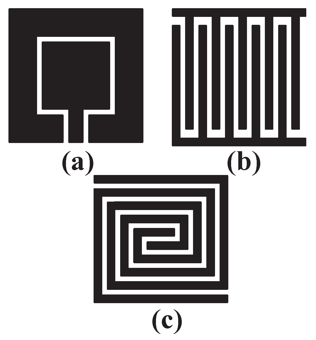
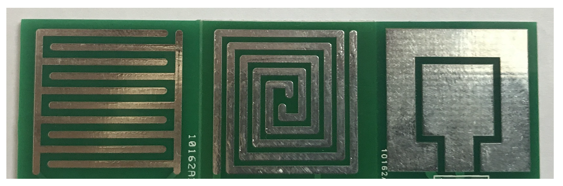
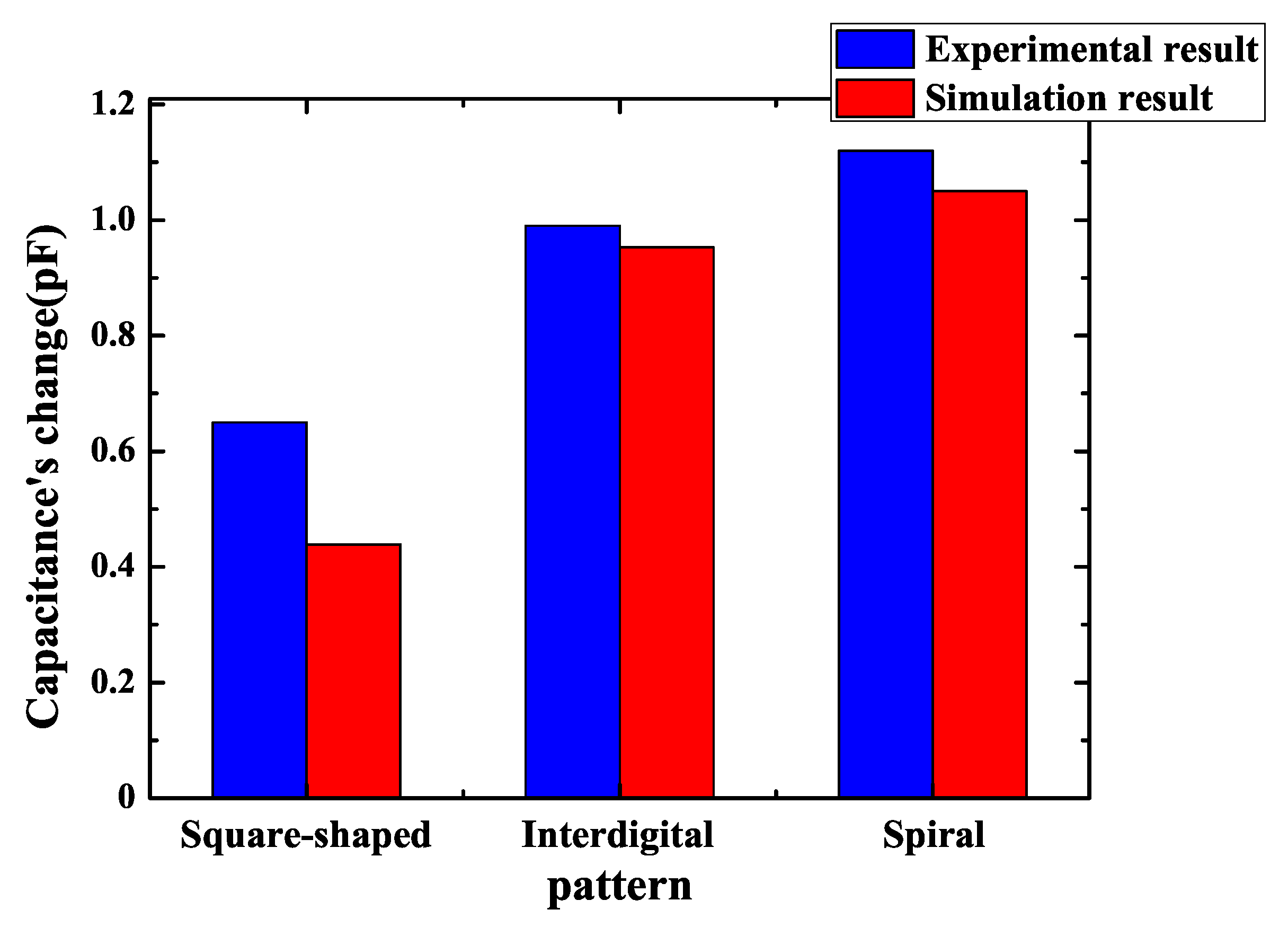
3.1. Influence of the Fringing Electric Field Sensor’s Pattern
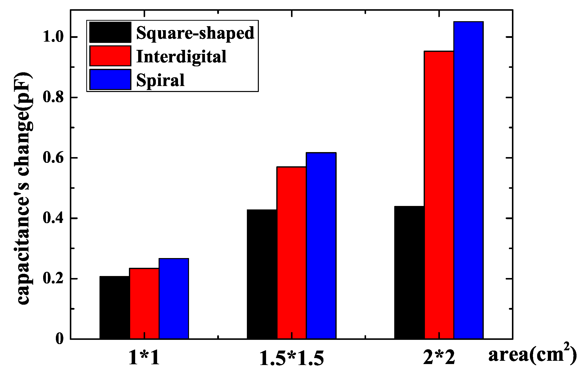
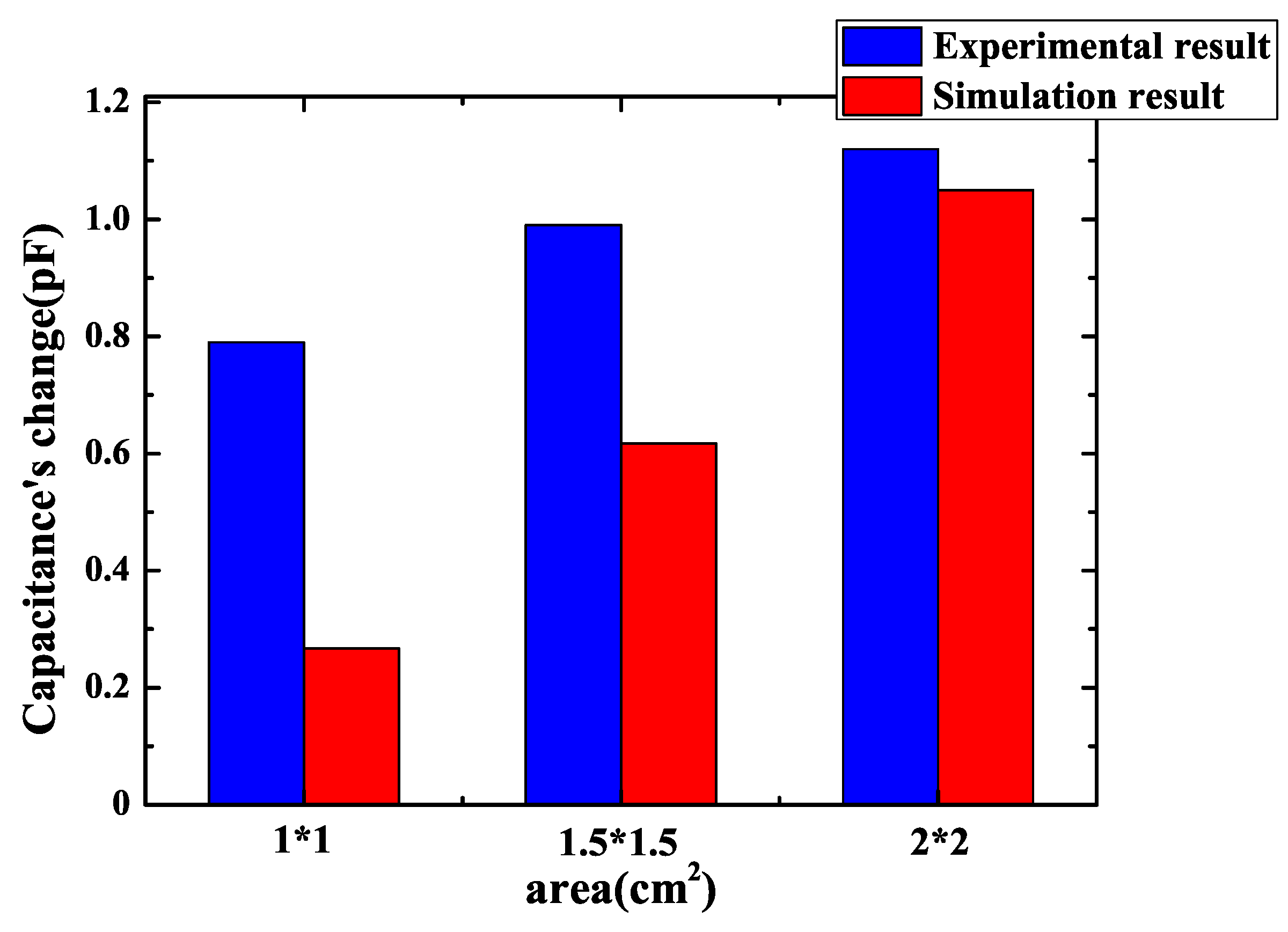
3.2. Influence of a Fringing Electric Field Sensor’s Area
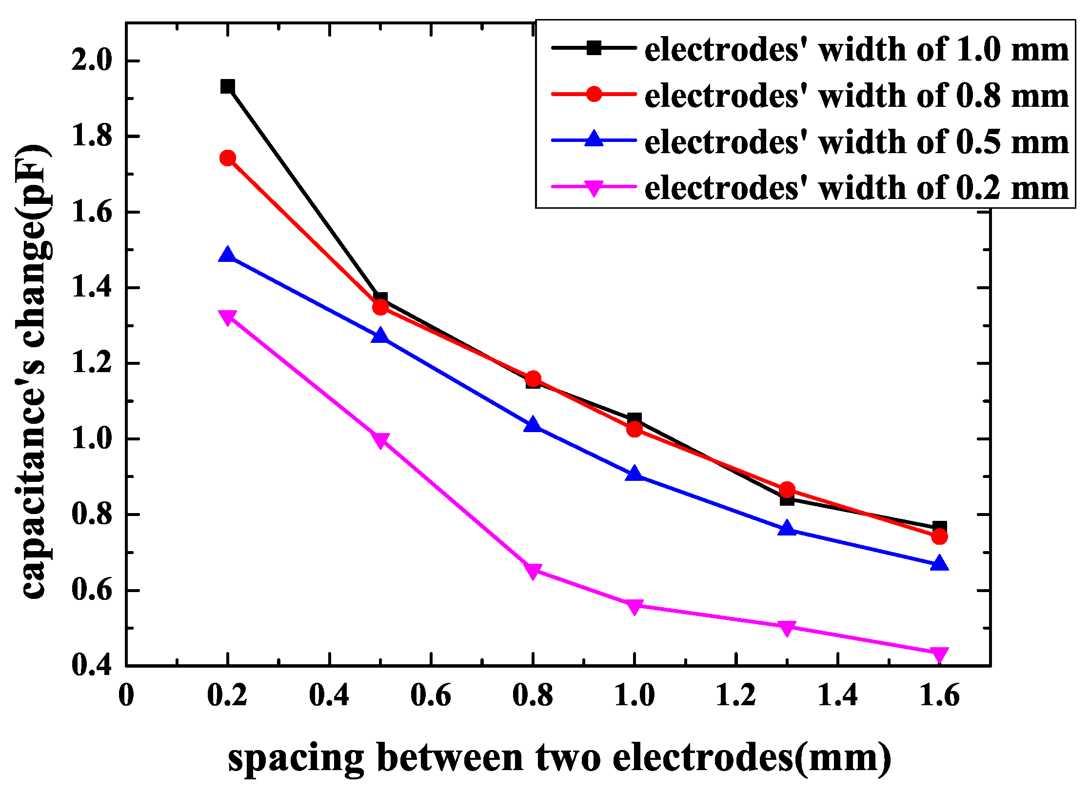
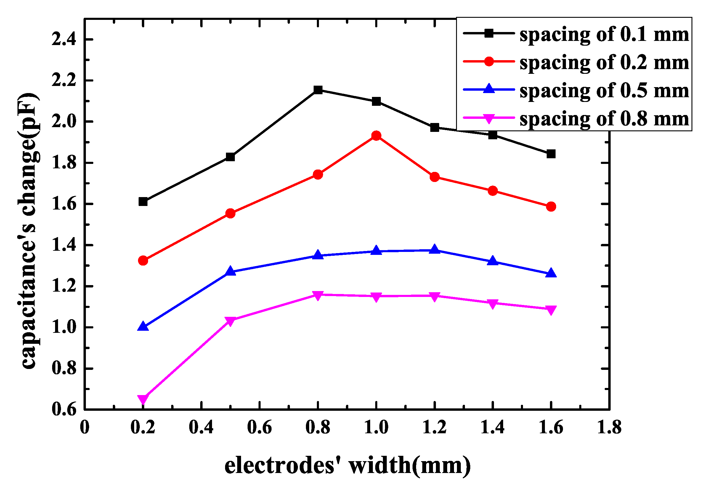
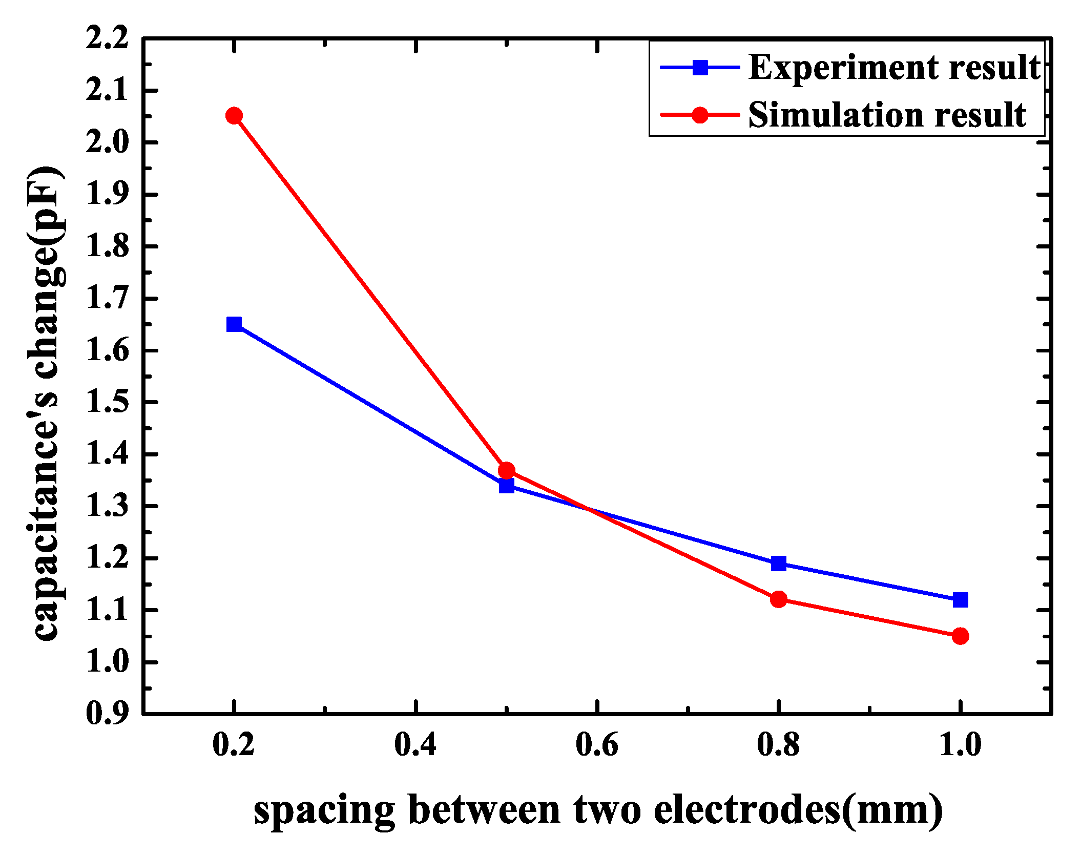
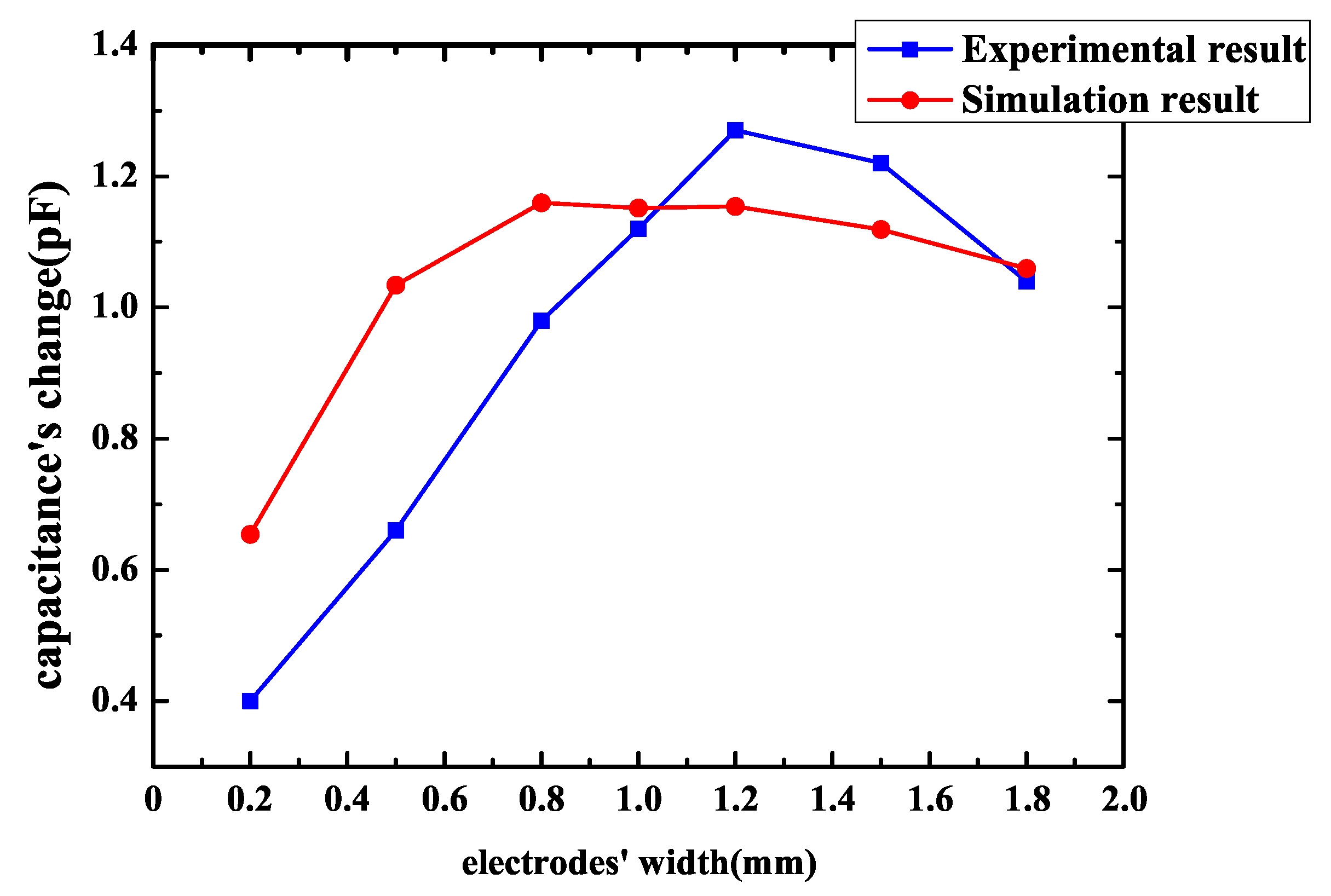
3.3. Influence of Fringing Electric Field Sensor’s Geometrical Parameters
4. Experimental Results and Discussion
4.1. Experiment Process and Results
4.2. Discussion
5. Conclusions
Author Contributions
Funding
Conflicts of Interest
References
- Ray, S.; Peeters, E.; Tehranipoor, M.M.; Bhunia, S. System-on-Chip Platform Security Assurance: Architecture and Validation. Proc. IEEE 2018, 1, 21–37. [Google Scholar] [CrossRef]
- Miura, N.; Fujimoto, D.; Hayashi, Y.I.; Homma, N.; Aoki, T.; Nagata, M. Integrated-circuit countermeasures against information leakage through EM radiation. In Proceedings of the IEEE International Symposium on Electromagnetic Compatibility, Raleigh, NC, USA, 4–8 August 2014; pp. 748–751. [Google Scholar] [CrossRef]
- Shahrjerdi, D.; Rajendran, J.; Garg, S.; Koushanfar, F.; Karri, R. Shielding and securing integrated circuits with sensors. In Proceedings of the IEEE/ACM International Conference on Computer-Aided Design, San Jose, CA, USA, 2–6 November 2014; pp. 170–174. [Google Scholar] [CrossRef]
- Torii, N.; Yamamoto, D.; Takenaka, M.; Matsumoto, T. Experimental Evaluation on the Resistance of Latch PUFs Implemented on ASIC against FIB-Based Invasive Attacks. IEICE Trans. Fundam. 2016, E99.A, 118–129. [Google Scholar] [CrossRef]
- Skorobogatov, S. Using optical emission analysis for estimating contribution to power analysis. In Proceedings of the 2009 Workshop on Fault Diagnosis and Tolerance in Cryptography, Lausanne, Switzerland, 6 September 2009; pp. 111–119. [Google Scholar] [CrossRef]
- Wang, T.; Xu, S.; Lv, D.; Teng, J.; Zeng, S.; Zhang, H. Tamper Device for Active RFID Electronic Tag. China Patent CN104573795 (A), 29 April 2015. [Google Scholar]
- Skorobogatov, S. Optical Fault Masking Attacks. In Proceedings of the 2010 Workshop on Fault Diagnosis and Tolerance in Cryptography, Santa Barbara, CA, USA, 21 August 2010; pp. 23–29. [Google Scholar] [CrossRef]
- Hao, X.; Zhang, J.; Wu, X. Ultrahigh Frequency Anti Metal Electronic Label Structure with Anti-Tearing Function. China Patent CN202102475 (U), 4 January 2012. [Google Scholar]
- Lee, H.K.; Chang, S.I.; Yoo, E. Dual-Mode Capacitive Proximity Sensor for Robot Application: Implementation of Tactile and Proximity Sensing Capability on a Single Polymer Platform Using Shared Electrodes. IEEE Sens. J. 2009, 9, 1748–1755. [Google Scholar] [CrossRef]
- Mizuguchi, J.; Piai, J.C.; França, J.A.D.; França, M.B.D.M.; Yamashita, K.; Mathias, L.C. Fringing Field Capacitive Sensor for Measuring Soil Water Content: Design, Manufacture, and Testing. IEEE Trans. Instrum. Meas. 2015, 64, 212–220. [Google Scholar] [CrossRef]
- Noltingk, B.E. A novel proximity gauge. J. Phys. E Sci. Instrum. 1969, 2, 356–360. [Google Scholar] [CrossRef]
- Wang, H.C.; Zyuzin, A.; Mamishev, A.V. Measurement of Coating Thickness and Loading Using Concentric Fringing Electric Field Sensors. IEEE Sens. J. 2014, 14, 68–78. [Google Scholar] [CrossRef]
- Mcintosh, R.B.; Casada, M.E. Fringing Field Capacitance Sensor for Measuring the Moisture Content of Agricultural Commodities. IEEE Sens. J. 2008, 8, 240–247. [Google Scholar] [CrossRef]
- Langfelder, G.; Longoni, A.F.; Tocchio, A.; Lasalandra, E. MEMS Motion Sensors Based on the Variations of the Fringe Capacitances. IEEE Sens. J. 2011, 11, 1069–1077. [Google Scholar] [CrossRef]
- Da, C.E.; de Oliveira, N.E.; Morais, F.J.O.; Carvalhaesdias, P.; Duarte, L.F.C.; Cabot, A.; Siqueira, D.J.A. A Self-Powered and Autonomous Fringing Field Capacitive Sensor Integrated into a Micro Sprinkler Spinner to Measure Soil Water Content. Sensors 2017, 17, 575. [Google Scholar] [CrossRef]
- Li, X.B.; Larson, S.D.; Zyuzin, A.S.; Mamishev, A.V. Design of multichannel fringing electric field sensors for imaging. Part I. General design principles. In Proceedings of the Conference Record of the 2004 IEEE International Symposium on Electrical Insulation, Indianapolis, IN, USA, 19–22 September 2004; pp. 406–409. [Google Scholar]
- Shan, M.; Min, R.; Zhong, Z.; Wang, Y.; Zhang, Y. Differential reflective fiber-optic angular displacement sensor. Opt. Laser Technol. 2015, 68, 124–128. [Google Scholar] [CrossRef]
- Li, X.; Rowe, G.; Inclan, V.; Mamishev, A.V. Nondimensionalized Parametric Modeling of Fringing Electric-Field Sensors. IEEE Sens. J. 2006, 6, 1602–1608. [Google Scholar] [CrossRef]
- Pandey, S.S.; Mastrangelo, C.H. An Exothermal Energy Release Layer for Microchip Transience. In Proceedings of the 2013 IEEE Sensors, Baltimore, MD, USA, 3–6 July 2013; pp. 1–4. [Google Scholar] [CrossRef]
- Banerjee, N.; Xie, Y.; Rahman, M.M.; Kim, H.; Mastrangelo, C.H. From Chips to Dust: The Mems Shatter Secure Chip. In Proceedings of the 2014 IEEE 27th International Conference on Micro Electro Mechanical Systems, San Francisco, CA, USA, 26–30 January 2014; pp. 1123–1126. [Google Scholar] [CrossRef]
- Dean, R.N.; Rane, A.K.; Baginski, M.E.; Richard, J.; Hartzog, Z.; Elton, D.J. A Capacitive Fringing Field Sensor Design for Moisture Measurement Based on Printed Circuit Board Technology. IEEE Trans. Instrum. Meas. 2012, 61, 1105–1112. [Google Scholar] [CrossRef]
- Peng, F.; Lv, Y.; Li, H.; Tian, S.; Chen, W.; Yang, J. Sensitivity Prediction of Multiturn Fiber Coil-based Fiber-optic Flexural Disk Seismometer via Finite Element Method Analysis. J. Lightw. Technol. 2017, 35, 3870–6876. [Google Scholar] [CrossRef]
- Ma, C.; Huang, Z.; Wang, Z.; Zhou, L.; Li, Y. An energy efficient technique using electric active shielding for capacitive coupling intra-body communication. Sensors 2017, 17, 2056. [Google Scholar] [CrossRef] [PubMed]
- Andrews, J.B.; Cao, C.; Brooke, M.A.; Franklin, A.D. Noninvasive material thickness detection by aerosol jet printed sensors enhanced through metallic carbon nanotube ink. IEEE Sens. J. 2017, 17, 4612–4618. [Google Scholar] [CrossRef]
- Chen, Z.; Luo, R.C. Design and implementation of capacitive proximity sensor using microelectromechanical systems technology. IEEE Trans. Ind. Electron. 1998, 45, 886–894. [Google Scholar] [CrossRef]
- Chang, X.M.; Dou, Y.; Zhuo, D.; Fan, J.H. Research on Sensor of Ice Layer Thickness Based on Effect of Fringe Electric Field. In Proceedings of the 2012 International Conference on Computing, Measurement, Control and Sensor Network, Taiyuan, China, 7–9 July 2012; pp. 417–420. [Google Scholar] [CrossRef]


| Pattern | Area (cm) | Electrode Spacing (mm) | Electrode Width (mm) | Number of Fingers or Loops |
|---|---|---|---|---|
| Square-shaped | 1 × 1 | 1 | N/A | N/A |
| Square-shaped | 1.5 × 1.5 | 1 | N/A | N/A |
| Square-shaped | 2 × 2 | 1 | N/A | N/A |
| Interdigitated | 1 × 1 | 1 | 1 | 5 |
| Interdigitated | 1.5 × 1.5 | 1 | 1 | 8 |
| Interdigitated | 2 × 2 | 1 | 1 | 10 |
| Spiral | 1 × 1 | 1 | 1 | 3 |
| Spiral | 1.5 × 1.5 | 1 | 1 | 4 |
| Spiral | 2 × 2 | 1 | 1 | 5 |
| Electrode Width (mm) | 0.2 | 0.5 | 0.8 | 1 | 1.2 | 1.4 | 1.6 | ||
|---|---|---|---|---|---|---|---|---|---|
| Number of Loops | |||||||||
| Electrode Spacing (mm) | |||||||||
| 0.1 | 33 | 16 | 10 | 9 | 7 | 6 | 5 | ||
| 0.2 | 25 | 14 | 10 | 8 | 7 | 6 | 5 | ||
| 0.5 | 14 | 10 | 7 | 7 | 6 | 5 | 4 | ||
| 0.8 | 10 | 8 | 6 | 6 | 5 | 5 | 4 | ||
| 1 | 9 | 7 | 6 | 3 | N/A | N/A | N/A | ||
| 1.3 | 7 | 6 | 3 | 3 | N/A | N/A | N/A | ||
| 1.6 | 6 | 5 | 3 | 3 | N/A | N/A | N/A | ||
| Pattern | Area (cm) | Electrode Spacing (mm) | Electrode Width (mm) | Number of Fingers or Loops |
|---|---|---|---|---|
| Square-shaped | 2 × 2 | 1 | N/A | N/A |
| Interdigitated | 2 × 2 | 1 | 1 | 10 |
| Spiral | 2 × 2 | 1 | 1 | 5 |
| Pattern | Area (cm) | Electrode Spacing (mm) | Electrode Width (mm) | Number of Loops |
|---|---|---|---|---|
| Interdigitated | 1 × 1 | 1 | 1 | 3 |
| Interdigitated | 1.5 × 1.5 | 1 | 1 | 4 |
| Interdigitated | 2 × 2 | 1 | 1 | 5 |
| Pattern | Area (cm) | Electrode Spacing (mm) | Electrode Width (mm) | Number of Loops |
|---|---|---|---|---|
| Interdigitated | 2 × 2 | 0.2 | 1 | 8 |
| Interdigitated | 2 × 2 | 0.5 | 1 | 7 |
| Interdigitated | 2 × 2 | 0.8 | 1 | 6 |
| Interdigitated | 2 × 2 | 1 | 1 | 5 |
| Pattern | Area (cm) | Electrode Spacing (mm) | Electrode Width (mm) | Number of Loops |
|---|---|---|---|---|
| Interdigitated | 2 × 2 | 0.8 | 0.2 | 10 |
| Interdigitated | 2 × 2 | 0.8 | 0.5 | 8 |
| Interdigitated | 2 × 2 | 0.8 | 0.8 | 6 |
| Interdigitated | 2 × 2 | 0.8 | 1 | 6 |
| Interdigitated | 2 × 2 | 0.8 | 1.2 | 5 |
| Interdigitated | 2 × 2 | 0.8 | 1.5 | 5 |
| Interdigitated | 2 × 2 | 0.8 | 1.8 | 4 |
© 2018 by the authors. Licensee MDPI, Basel, Switzerland. This article is an open access article distributed under the terms and conditions of the Creative Commons Attribution (CC BY) license (http://creativecommons.org/licenses/by/4.0/).
Share and Cite
Gao, X.; Zhao, Y.; Ma, H. Fringing Electric Field Sensors for Anti-Attack at System-Level Protection. Sensors 2018, 18, 3034. https://doi.org/10.3390/s18093034
Gao X, Zhao Y, Ma H. Fringing Electric Field Sensors for Anti-Attack at System-Level Protection. Sensors. 2018; 18(9):3034. https://doi.org/10.3390/s18093034
Chicago/Turabian StyleGao, Xiang, Yiqiang Zhao, and Haocheng Ma. 2018. "Fringing Electric Field Sensors for Anti-Attack at System-Level Protection" Sensors 18, no. 9: 3034. https://doi.org/10.3390/s18093034
APA StyleGao, X., Zhao, Y., & Ma, H. (2018). Fringing Electric Field Sensors for Anti-Attack at System-Level Protection. Sensors, 18(9), 3034. https://doi.org/10.3390/s18093034