Multilayer Black Phosphorus Near-Infrared Photodetectors


 and
and 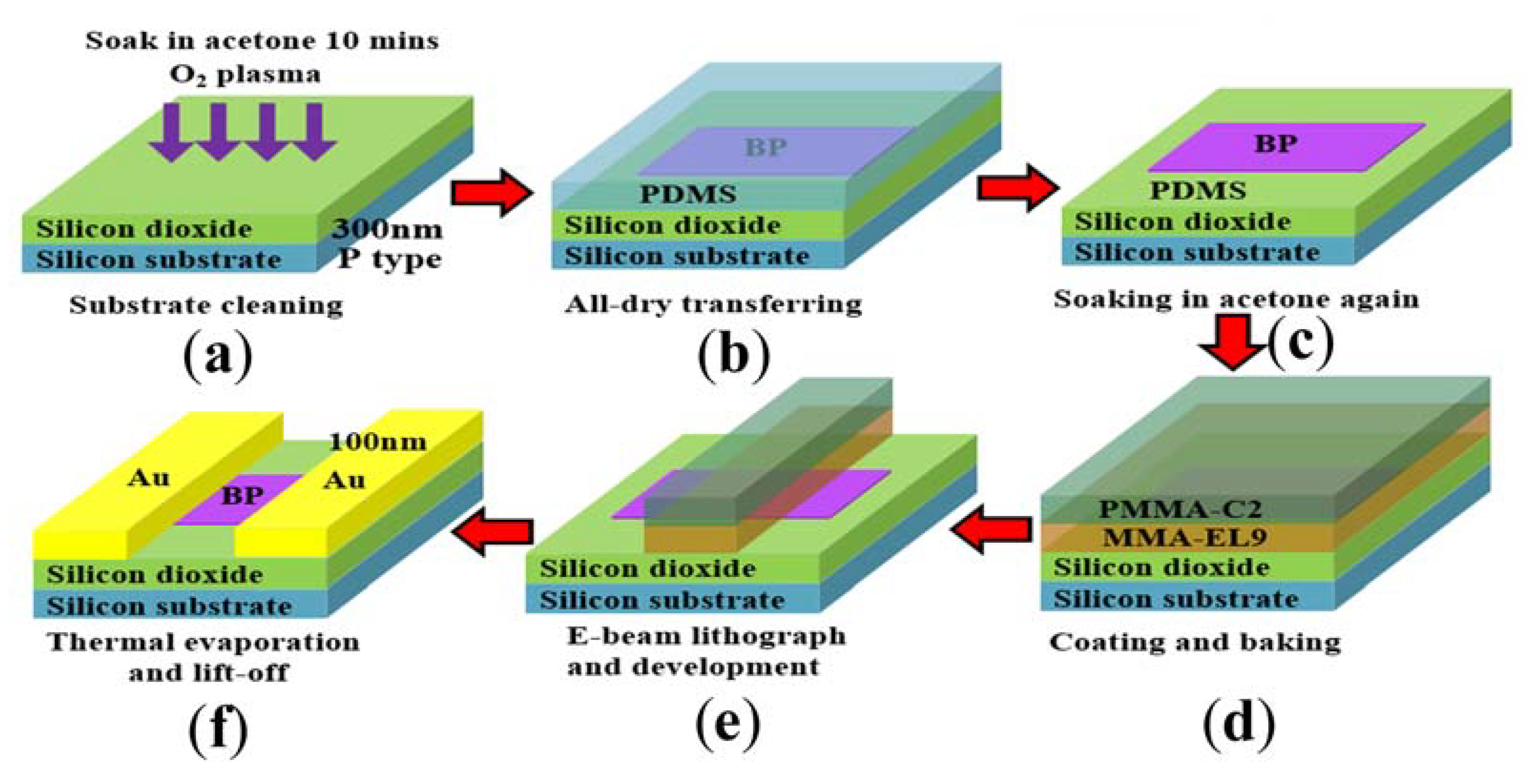
Abstract
:1. Introduction
2. Materials and Methods
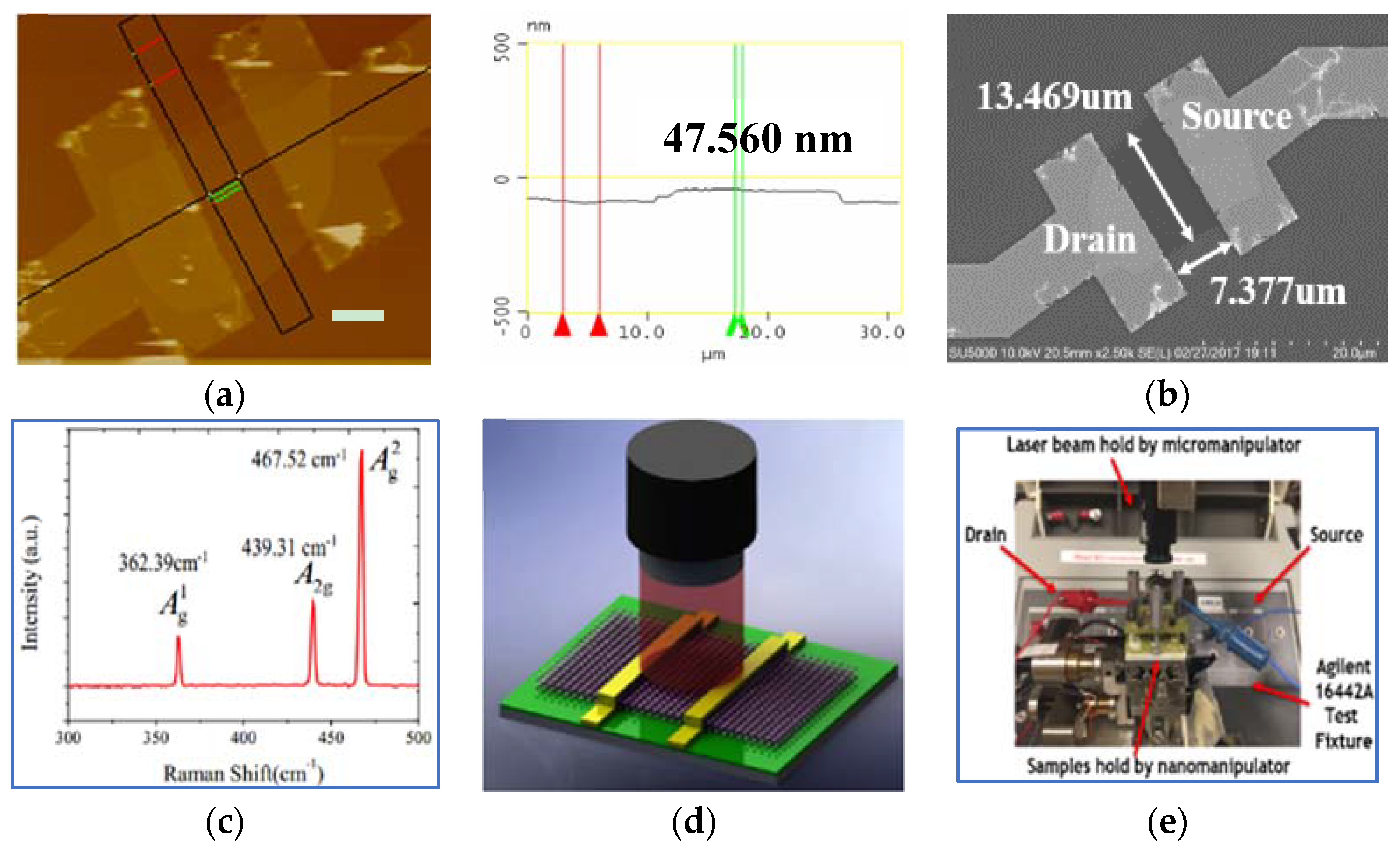
2.1. Preparation of the BP Nanoflakes
2.2. Fabrication of the BP FETs
2.3. Characterization and Measurements of BP FETs
3. Results
3.1. Thickness-Dependence Electron Transport Performance of BP FETs
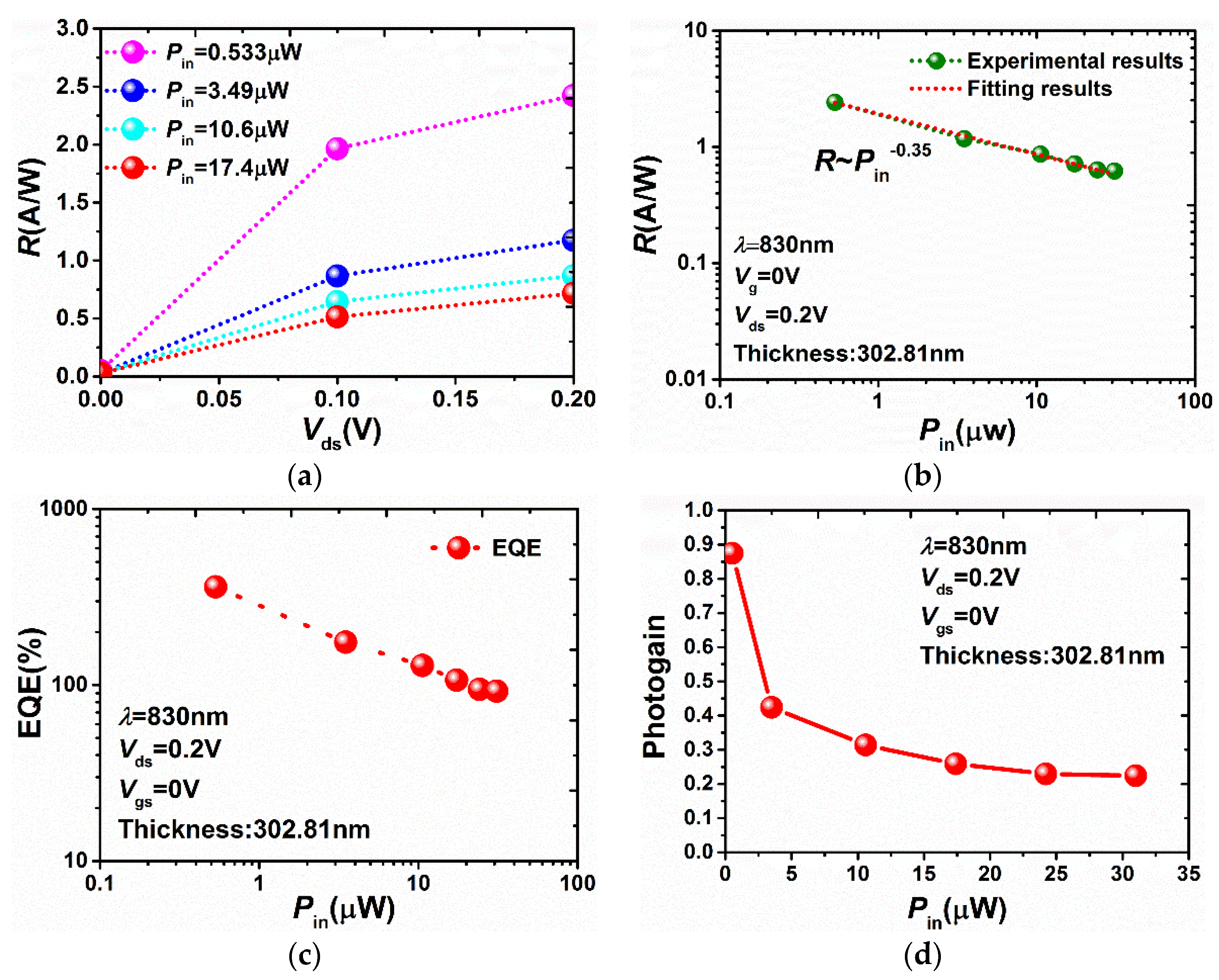
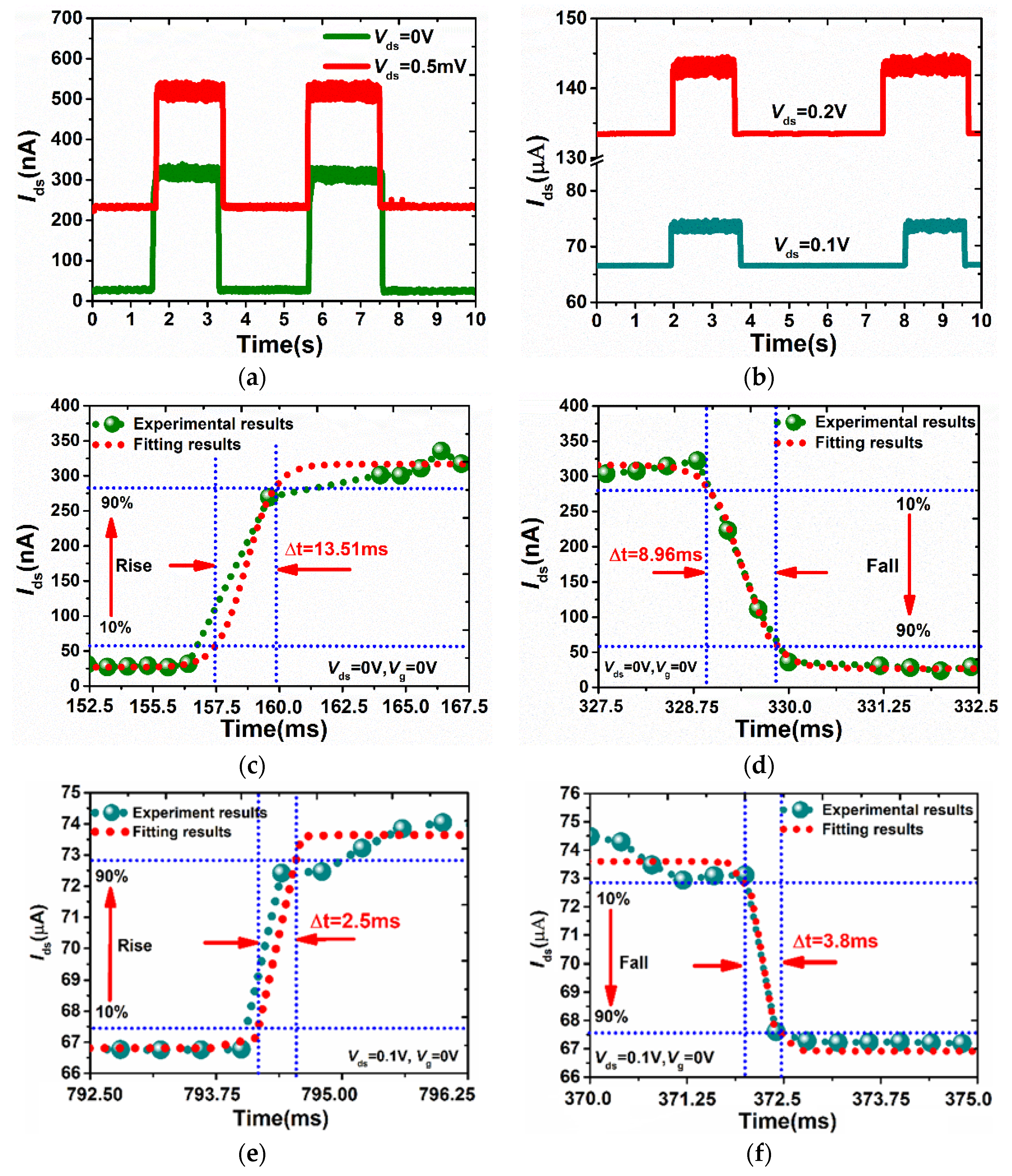
3.2. Photo-Response of Multilayer BP Photodetectors
4. Conclusions
Author Contributions
Funding
Acknowledgments
Conflicts of Interest
References
- Yuichi, A.; Endo, S.; Narita, S.I. Electrical properties of black phosphorus single crystals. J. Phys. Soc. Jpn. 1983, 52, 2148–2155. [Google Scholar] [CrossRef]
- Qiao, J.; Kong, X.; Hu, Z.X.; Yang, F.; Ji, W. High-mobility transport anisotropy and linear dichroism in few-layer black phosphorus. Nat. Commun. 2014, 4475. [Google Scholar] [CrossRef] [PubMed]
- Kong, L.; Qin, Z.; Xie, G.; Guo, Z.; Zhang, H.; Yuan, P.; Qian, L. Black phosphorus as broadband saturable absorber for pulsed lasers from 1 μm to 2.7 μm wavelength. Laser Phys. Lett. 2016, 13. [Google Scholar] [CrossRef]
- Huang, M.; Wang, M.; Chen, C.; Ma, Z.; Li, X.; Han, J.; Wu, Y. Broadband Black-Phosphorus Photodetectors with High Responsivity. Adv. Mater. 2016, 28, 3481–3485. [Google Scholar] [CrossRef] [PubMed]
- Michele, B.; Dirk, J.G.; Sofya, I.B.; Gary, A.S.; Ver der zant, H.S.J.; Andres, C.G. Fast and broadband photo-response of few-layer black phosphorus field-effect transistors. Nano Lett. 2014, 14, 3347–3352. [Google Scholar] [CrossRef]
- Island, J.O.; Steele, G.A.; Ver der zant, H.S.J.; Andres, C.G. Environmental instability of few-layer black phosphorus. 2D Mater. 2015, 2, 011002. [Google Scholar] [CrossRef]
- Zhou, Q.H.; Chen, Q.; Tong, Y.; Wang, J. Light-Induced Ambient Degradation of Few-Layer Black Phosphorus: Mechanism and Protection. Angew. Chem. 2016, 128, 11609–11613. [Google Scholar] [CrossRef]
- Low, T.; Engel, M.; Steiner, M.; Avouris, P. Origin of photoresponse in black phosphorus phototransistors. Phys. Rev. B 2014, 90. [Google Scholar] [CrossRef]
- Gomez, A.C.; Buscema, M.; Molenaar, R.; Singh, V.; Janssen, L.; van der Zant, H.S.J.; Steele, G.A. Deterministic Transfer of Two-dimensional Materials by All-Dry Viscoelastic Stamping. 2D Mater. 2014, 1. [Google Scholar] [CrossRef]
- Sui, Y.; Appenzella, J. Screening and Interlayer Coupling in Multilayer Graphene Field-Effect Transistors. Nano Lett. 2009, 9, 2973–2977. [Google Scholar] [CrossRef] [PubMed]
- Rodin, A.S.; Carvalho, A.; Neto, A.H.C. Strain-Induced Gap Modification in Black Phosphorus. Phys. Rev. Lett. 2014, 112. [Google Scholar] [CrossRef] [PubMed]
- Liu, X.C.; Qu, D.S.; Li, H.M.; Moon, I.; Ahmed, F.; Kim, C.; Lee, M.; Choi, Y.; Cho, J.H.; Hone, J.C.; et al. Modulation of Quantum Tunneling via a Vertical Two-Dimensional Black Phosphorus and Molybdenum Disulfide p−n Junction. ACS Nano 2017, 11, 9143–9150. [Google Scholar] [CrossRef] [PubMed]
- Das, S.; Chen, H.Y.; Penumatcha, A.V.; Appenzeller, J. High performance multilayer MoS2 transistors with scandium contacts. Nano Lett. 2013, 13, 100–105. [Google Scholar] [CrossRef] [PubMed]
- Wang, H.M.; Wu, Y.H.; Cong, C.X.; Shang, J.Z.; Yu, T. Hysteresis of Electronic Transport in Graphene Transistors. Nano Lett. 2010, 4, 7221–7228. [Google Scholar] [CrossRef] [PubMed]
- Bube, R.H. Photoelectronic Properties of Semiconductors; Cambridge University Press: Cambridge, UK, 1992. [Google Scholar]
- Ye, L.; Li, H.; Chen, Z.; Xu, J. Near-Infrared Photodetector Based on MoS2/Black Phosphorus Heterojunction. ACS Photonics 2016, 3, 692–699. [Google Scholar] [CrossRef]
- Youngblood, N.; Li, M. Ultrafast photocurrent measurements of a black phosphorus photodetector. Appl. Phys. Lett. 2017, 110. [Google Scholar] [CrossRef]
- Oriol, L.S.; Lembke, D.; Kayci, M.; Radenovic, A.; Kis, A. Ultrasensitive photodetectors based on monolayer MoS2. Nat. Nanotechnol. 2013, 8, 497–501. [Google Scholar] [CrossRef]
- Gedrim, R.B.J.; Shanmugam, M.; Jain, N.; Christopher, A.D.; Michael, T.M.; Thomas, M.M.; Richard, J.M.; Richard, L.M.; Yu, B. Extraordinary Photoresponse in Two-Dimensional In2Se3 Nanosheets. ACS Nano 2013, 8, 514–521. [Google Scholar] [CrossRef] [PubMed]
- Hu, P.; Wang, L.; Yoon, M.; Zhang, J.; Feng, W.; Wang, X.; Wen, Z.; Idrobo, J.C.; Miyamoto, Y.; Eeohegan, D.B.; et al. Highly Responsive Ultrathin GaS Nanosheet Photodetectors on Rigid and Flexible Substrate. Nano Lett. 2013, 13, 1649–1654. [Google Scholar] [CrossRef] [PubMed]
- Tao, Y.; Wu, X.; Wang, W.; Wang, J. Flexible photodetector from ultraviolet to near infrared based on a SnS2 nanosheet microsphere film. J. Mater. Chem. C 2015, 3, 1347–1353. [Google Scholar] [CrossRef]
- Lai, K.W.C.; Xi, N.; Chen, H.; Fung, C.K.M.; Chen, L. Development of graphene-based optical detectors for infrared sensing applications. IEEE Sens. 2011, 398–401. [Google Scholar] [CrossRef]
- Yoo, J.; Jeong, S.; Kim, S.; Je, J.H. A stretchable nanowire UV–vis–NIR photodetector with high performance. Adv. Mater. 2015, 27, 1712–171722. [Google Scholar] [CrossRef] [PubMed]
- Tsai, D.S.; Liu, K.K.; Lien, D.H.; Tsai, M.L.; Kang, C.F.; Lin, C.A.; Li, L.J.; He, J.H. Few-Layer MoS2 with High Broadband Photogain and Fast Optical Switching for Use in Harsh Environments. ACS Nano 2013, 7, 3905–3911. [Google Scholar] [CrossRef] [PubMed]
- Wegrzecka, I.; Wegrzecki, M.; Grynglas, M.; Bar, J.; Uszynski, A.; Grodecki, R.; Grabiec, P.; Krzeminski, S.; Budzynski, T. Design and Properties of Silicon Avalanche Photodiodes. Opto-Electron. Rev. 2004, 12, 95–104. [Google Scholar]


© 2018 by the authors. Licensee MDPI, Basel, Switzerland. This article is an open access article distributed under the terms and conditions of the Creative Commons Attribution (CC BY) license (http://creativecommons.org/licenses/by/4.0/).
Share and Cite
Hou, C.; Yang, L.; Li, B.; Zhang, Q.; Li, Y.; Yue, Q.; Wang, Y.; Yang, Z.; Dong, L. Multilayer Black Phosphorus Near-Infrared Photodetectors. Sensors 2018, 18, 1668. https://doi.org/10.3390/s18061668
Hou C, Yang L, Li B, Zhang Q, Li Y, Yue Q, Wang Y, Yang Z, Dong L. Multilayer Black Phosphorus Near-Infrared Photodetectors. Sensors. 2018; 18(6):1668. https://doi.org/10.3390/s18061668
Chicago/Turabian StyleHou, Chaojian, Lijun Yang, Bo Li, Qihan Zhang, Yuefeng Li, Qiuyang Yue, Yang Wang, Zhan Yang, and Lixin Dong. 2018. "Multilayer Black Phosphorus Near-Infrared Photodetectors" Sensors 18, no. 6: 1668. https://doi.org/10.3390/s18061668
APA StyleHou, C., Yang, L., Li, B., Zhang, Q., Li, Y., Yue, Q., Wang, Y., Yang, Z., & Dong, L. (2018). Multilayer Black Phosphorus Near-Infrared Photodetectors. Sensors, 18(6), 1668. https://doi.org/10.3390/s18061668