Article

Second Generation Small Pixel Technology Using Hybrid Bond Stacking †

OmniVision Technologies, Inc., Santa Clara, CA 95054, USA
*
Author to whom correspondence should be addressed.
This paper is an extended version of our paper published in Venezia, V.C.; Shih, C.; Yang,W.-Z.; Zang, Y.; Lin, Z.; Grant, L.A.; Rhodes, H. 1.0 m pixel improvements with hybrid bond stacking technology. In Proceedings of the International Image Sensor Workshop, Hiroshima, Japan, 30 May–2 June 2017; pp. 8–11.
Sensors 2018, 18(2), 667; https://doi.org/10.3390/s18020667
Submission received: 2 November 2017 / Revised: 26 January 2018 / Accepted: 13 February 2018 / Published: 24 February 2018
(This article belongs to the Special Issue Special Issue on the 2017 International Image Sensor Workshop (IISW))

Abstract

:
In this work, OmniVision’s second generation (Gen2) of small-pixel BSI stacking technologies is reviewed. The key features of this technology are hybrid-bond stacking, deeper back-side, deep-trench isolation, new back-side composite metal-oxide grid, and improved gate oxide quality. This Gen2 technology achieves state-of-the-art low-light image-sensor performance for 1.1, 1.0, and 0.9 µm pixel products. Additional improvements on this technology include less than 100 ppm white-pixel process and a high near-infrared (NIR) QE technology.

1. Introduction

The first generation of back-side illuminated (BSI) stacked products used oxide bonding to physically bond wafers, and through-silicon vias (TSV) to form electrical connections [1,2]. In addition to the chip size reduction offered by wafer stacking, improvements in photo-diode performance are possible with “sensor only”-type processing that would negatively impact ASIC performance on non-stack BSI or even front-side illuminated sensors, such as new materials or thermal conditions [1]. In our second generation of stacking technologies, wafers are connected by the top-metal layer and the inter-layer dielectrics of the sensor and ASIC wafer, forming a hybrid oxide-oxide and metal-metal bond that physically and electrically connects the two wafers simultaneously. Hybrid bonding offers significant improvements in design and layout flexibility over the TSV stacking which consumes chip space to create deep vias and are aspect-ratio pitch limited; for examples, see Figure 1 and Figure 2. While TSVs can only be placed outside the array, hybrid-bond connections can be made both outside (Figure 2a) and inside the array (Figure 2b). In addition, hybrid bonding connections do not interfere with sensor or circuit performance, as is the case with the TSV Keep-Out Zone (KOZ) [3]. Using the flexibility hybrid bonding offers, the overall chip size of OmniVision’s 1 um, 16 MP stacked-chip product was reduced by ~10% [4].
Back-side, deep-trench isolation (BS-DTI), as well as a buried color filter array (CFA), were implemented in OmniVision’s first generation of stacking products to improve image quality [1]; BS-DTI to control electrical and optical crosstalk, and the buried CFA to reduce the optical stack height. Figure 3 is a cross section diagram comparing the Gen1 and Gen2 structures. In the Gen2 technology, the silicon thickness and the BS-DTI depth are increased to improve sensitivity while controlling crosstalk. A new composite oxide-metal grid (CMG) is introduced, in which an additional oxide-grid structure is added above the metal grid, separating neighboring color filters. As will be shown below, the Gen 2 pixel structure and process improves sensitivity without degrading crosstalk to achieve excellent low-light performance.

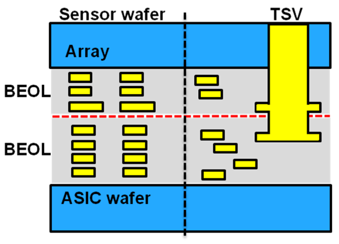
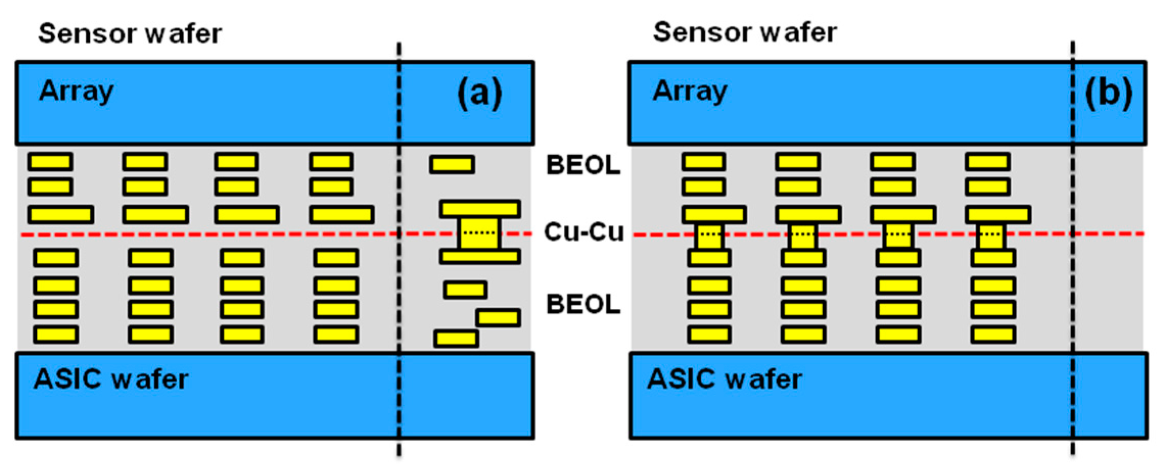
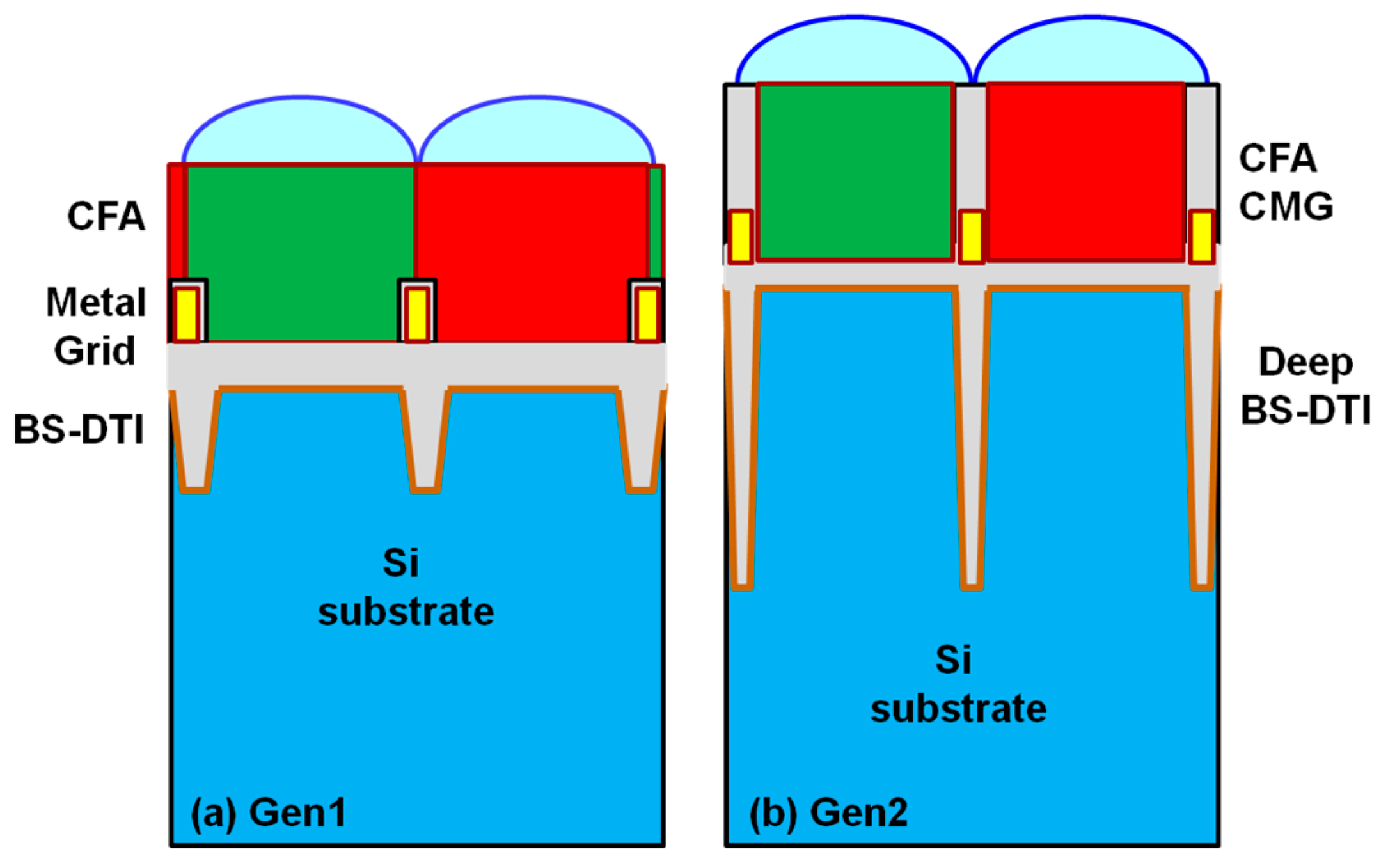
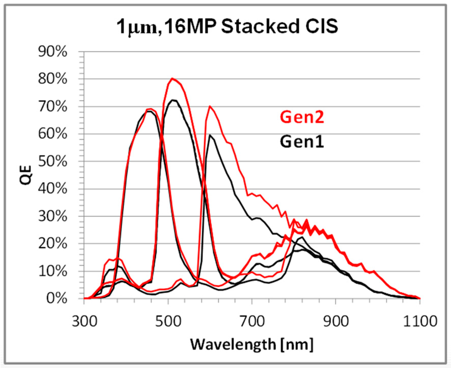
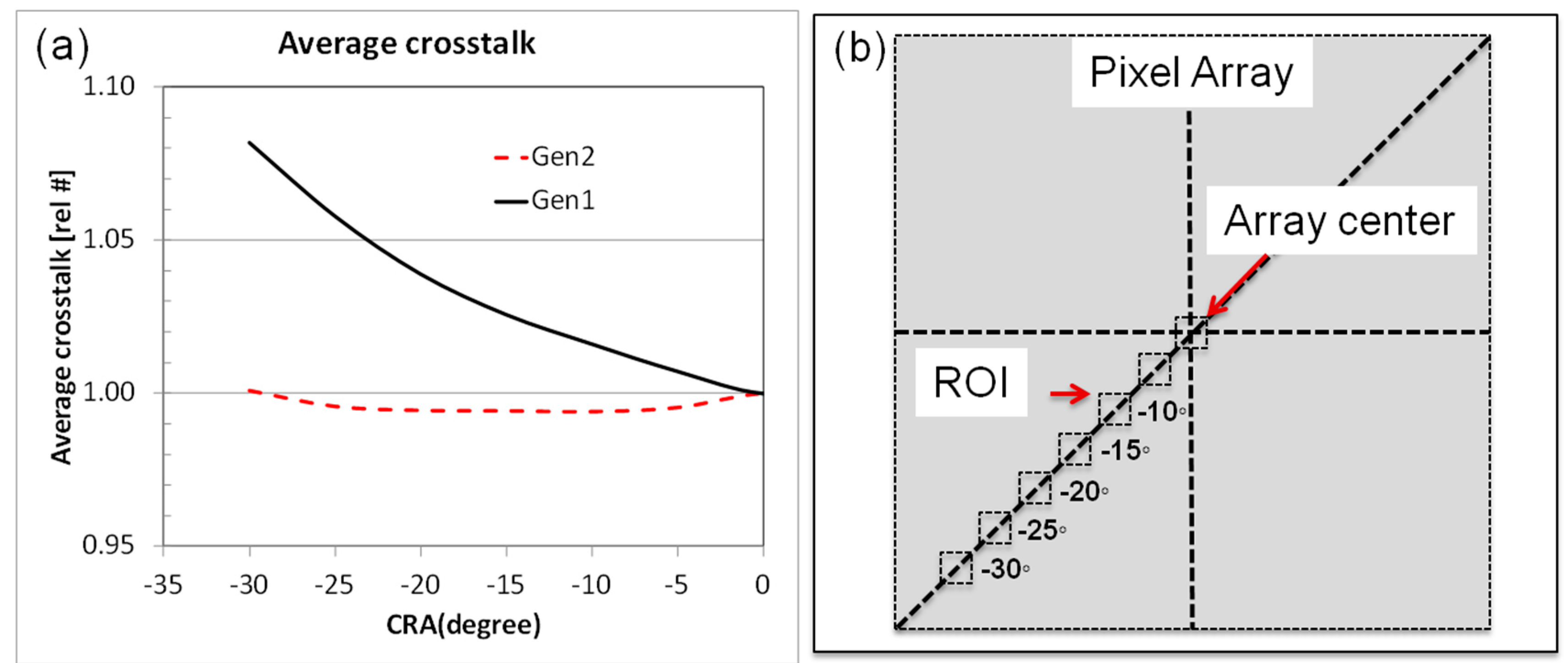
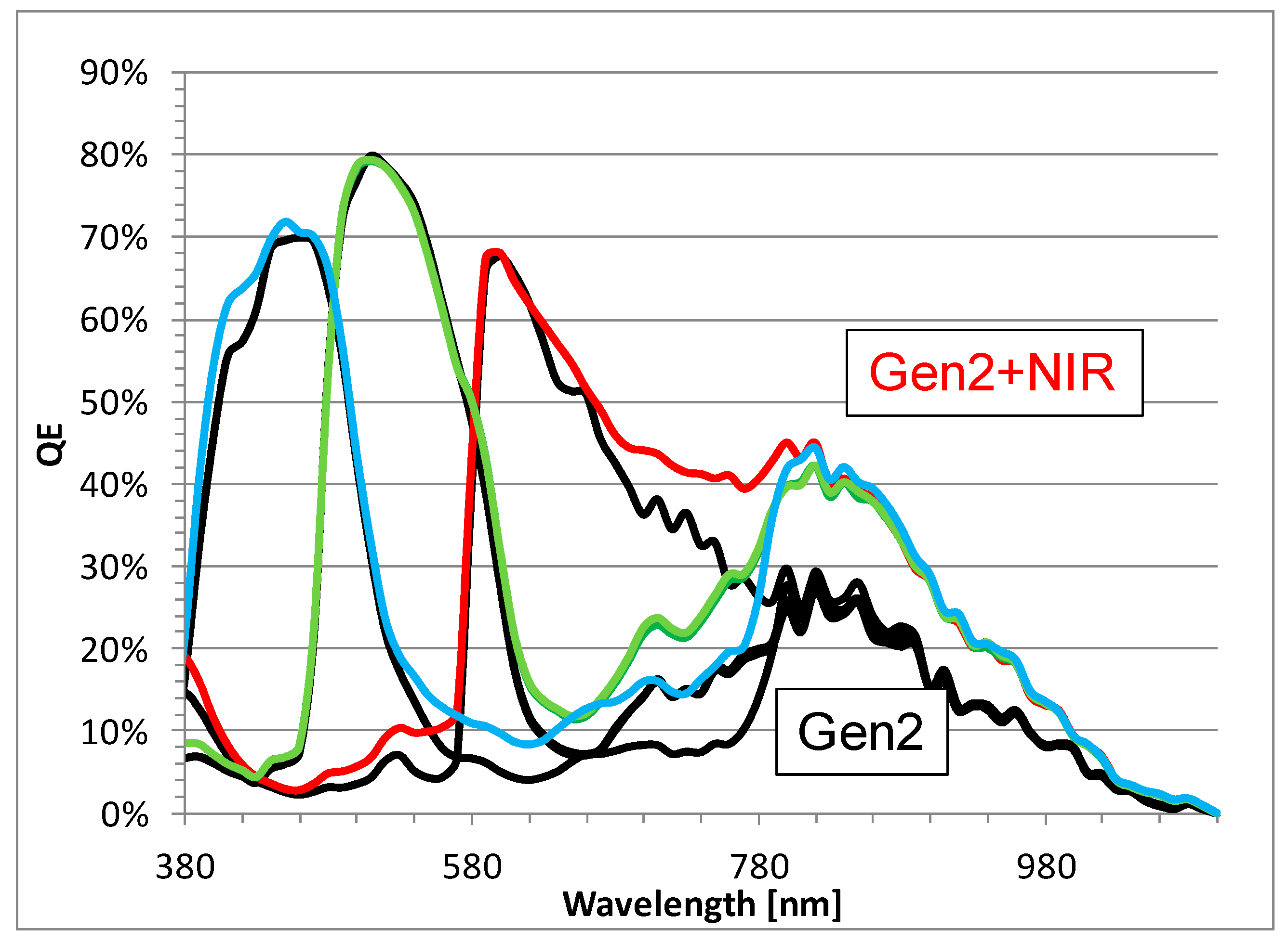
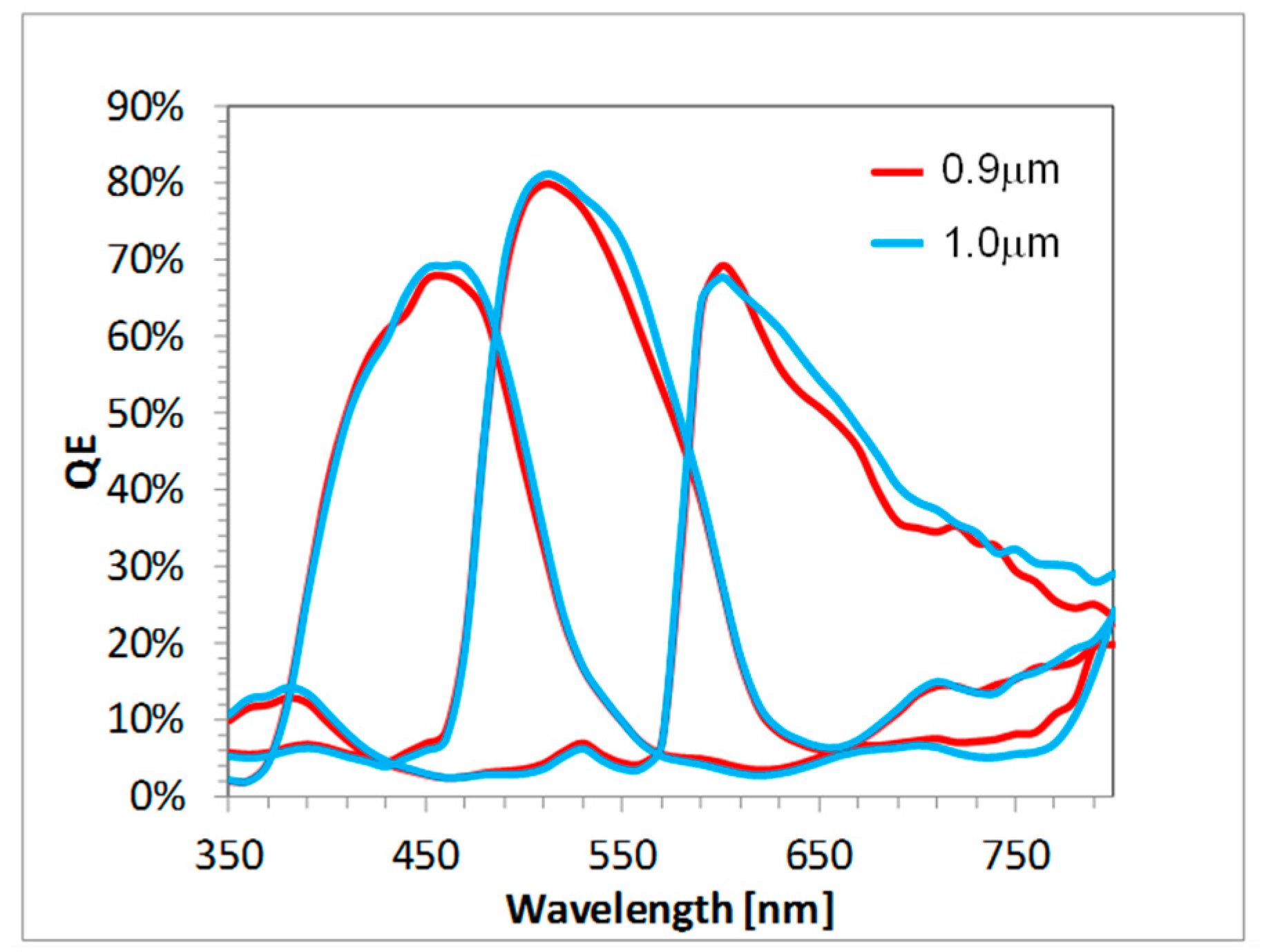
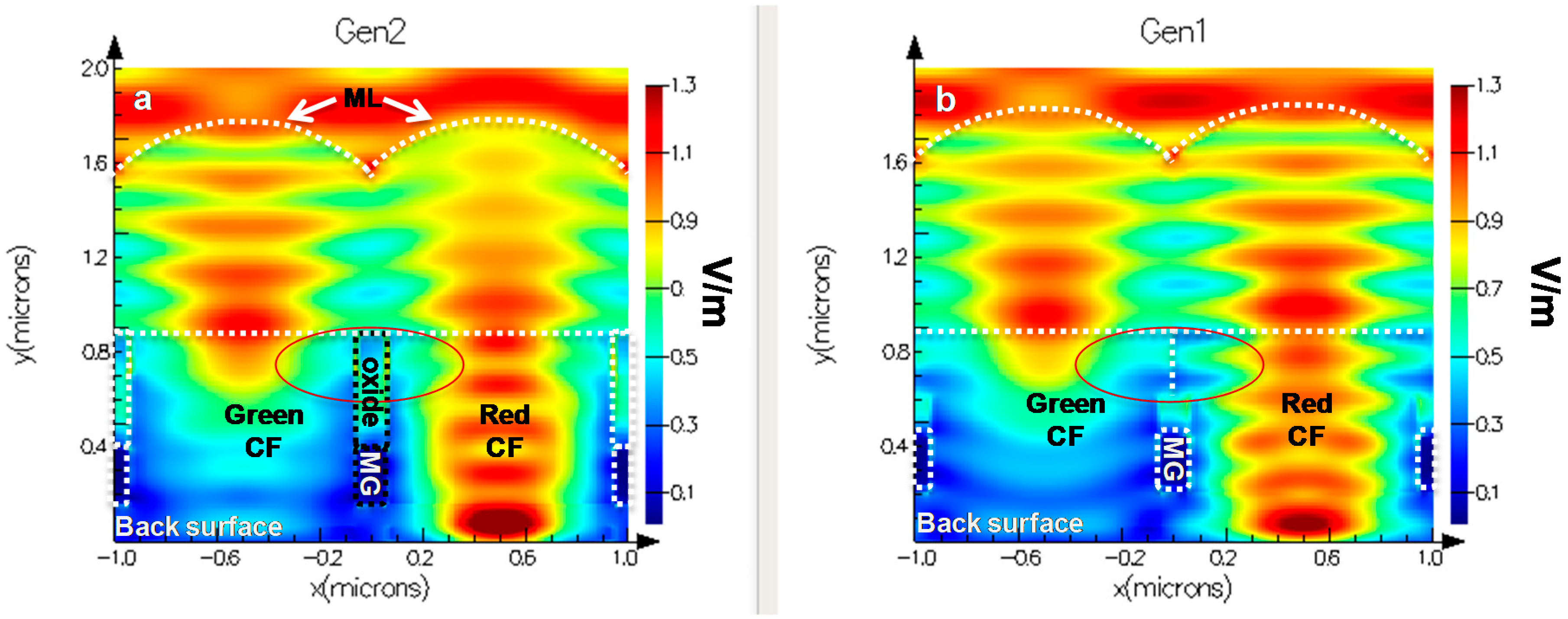
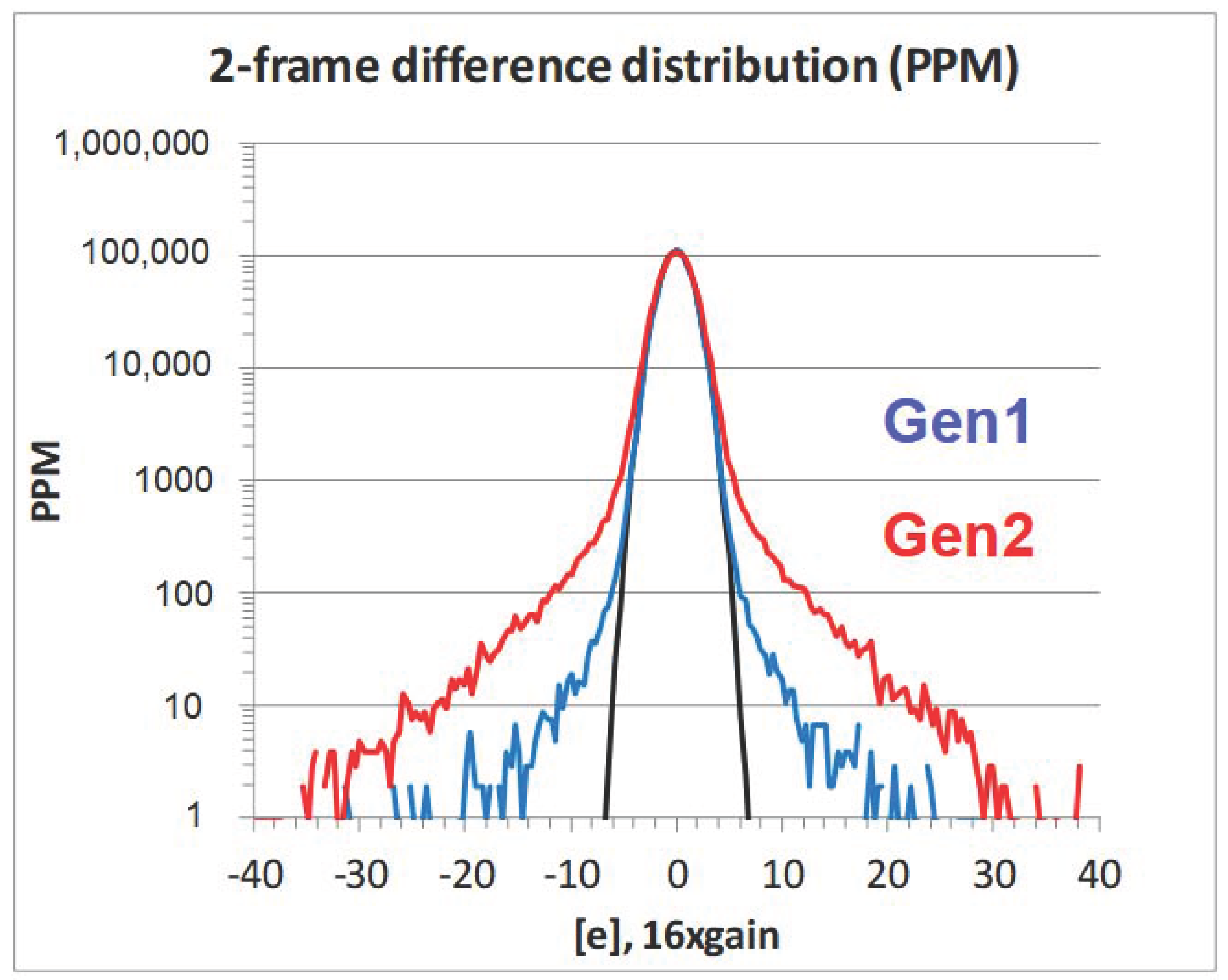
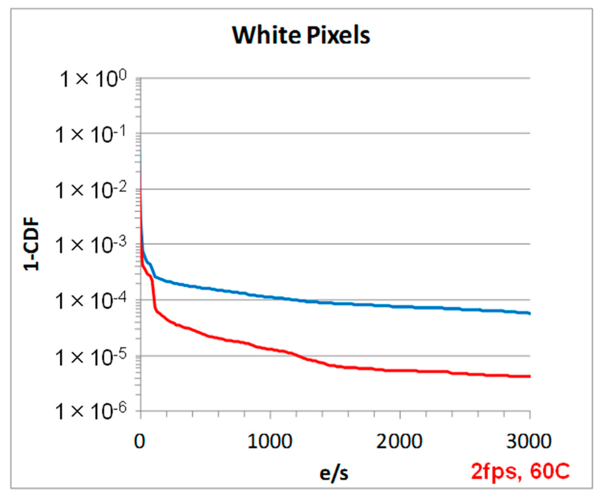
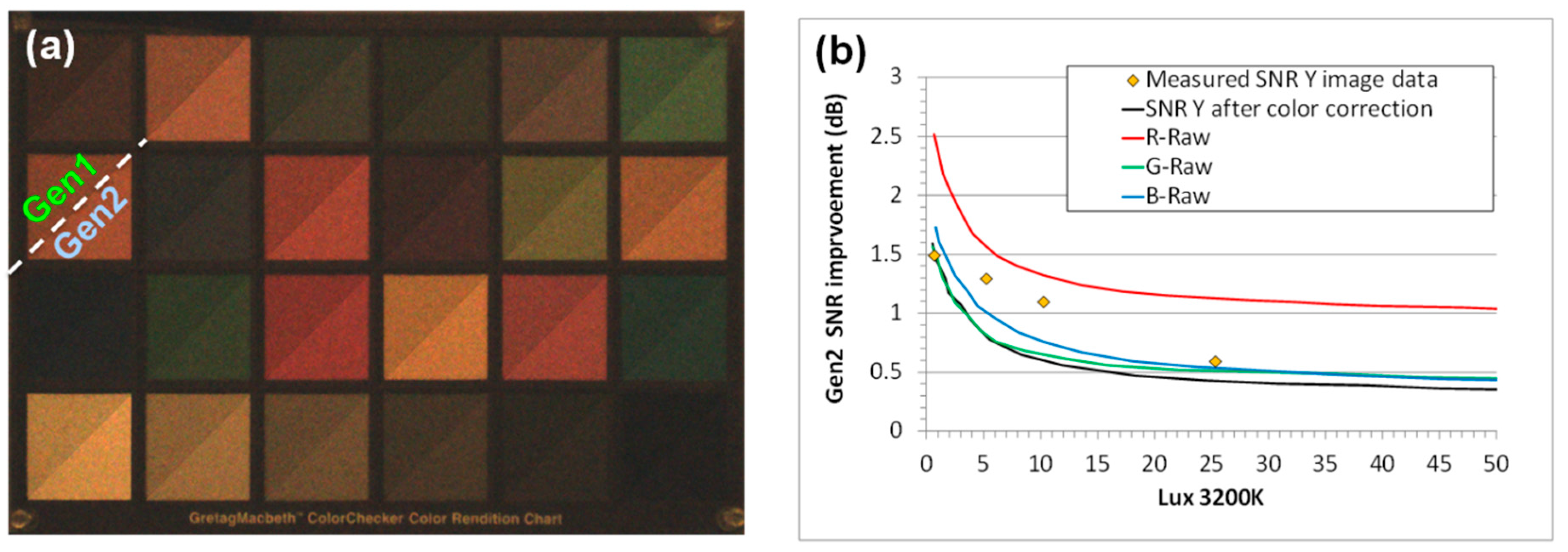
2. Results and Discussion

The quantum efficiency (QE) from 1 um, 16 MP Gen1 and Gen2 products is compared in Figure 4. The peak green and red QE are increased 10% and 15%, respectively, while the NIR QE (850 nm) is increased by ~50%. The Gen2 angular response improvement was reported in [4]. Figure 5a compares the Gen1 and Gen2 average crosstalk along the chief ray angle (CRA) of the sensor; crosstalk is calculated from QE measurements along a diagonal line from array center to edge, where the angle is determined by the CRA of the modules lens (Figure 5b). The crosstalk increases at large angles on a Gen1 sensor, while it remains relatively constant on a Gen2 stacked sensor. Figure 6 compares the QE from a 1.0 µm pixel CIS product to that from a 0.9 µm pixel CIS product, both using the Gen2 stacking technology described above. Despite the decrease in pixel size, the 0.9 µm pixel has the same high QE and low crosstalk as the 1.0 µm pixel, demonstrating that the Gen2 optical benefits can be extended to sub 1 µm pixel pitches.
Finite-difference time-domain (FDTD) simulations were used to understand the Gen2 improvement in optical performance. Figure 7 shows the simulation results comparing the Gen2 and Gen1 optical stacks. In the simulation, a 630 nm, monochromatic plane wave (Transverse electric mode (TM)) is used to illuminate neighboring pixels in each structure; the left pixel has a green color filter while the right pixel has a red color filter. The only difference between the pixels in each simulation is the color filter index of refraction. The figure plots the electric field propagation through the micro lens (ML) and color filter. The Gen1 and Gen2 structures are outlined by dashed lines and labeled for clarity. The main difference between structures is the extra silicon dioxide barrier between the color filters in the Gen2 stack. The silicon-dioxide refractive index (~1.45) is lower than that of the CF index (~1.6–2.0), resulting in light reflection at the CF/oxide interface. In the case of Gen1, partially filtered light can pass between color filters, resulting in signal loss due to optical crosstalk. The crosstalk difference is seen in the Figure 7 simulation results; comparing the circled areas, the electric field propagation between color filters is eliminated by the Gen2 CMG. The better light confinement in the CF by the CMG results in higher QE and lower optical crosstalk, which is consistent with the QE data in Figure 4.
In addition to the optical performance benefits, the Gen2 technology noise, white pixel (WP) and dark current performance has been improved over the Gen1, see Table 1. Figure 8 is a plot of the noise histogram from a two-frame difference image showing a ~2x improvement in the RTS noise. The low level of noise was achieved by maximizing the source follow area [5] and reducing source follower traps by minimizing etching damage, reducing dangling bonds, and by device channel engineering as discussed in [6]. The WP defect improvement is shown in Figure 9. A greater than 2x reduction in WP is achieved by engineering the photo-diode implant process to reduce any high electricity field regions and suppress the photo-diode (PD) depletion regions from interacting with high defect surfaces, such as front, back, and BS-DTI surfaces. The back surface passivation, for both Gen1 and Gen2, is achieved by deposition of a negatively charged oxide film [7]. In the Gen2 technology, the negative charge density in this film is increased, resulting in an improved dark current, as shown in Table 1.
The improved angular performance, as discussed in [4] and shown in Figure 5, is due to the BS-DTI. A relatively shallow BS-DTI was introduced in the Gen1 technology [1] and resulted in improvement in the crosstalk versus angle performance. This benefit was extended in Gen2 by increasing the DTI depth by ~3x, resulting in the elimination of the crosstalk at high angles (Figure 5).
It is well known that increasing the silicon thickness increases the long-wavelength QE [8]. As discussed above, the Gen2 thickness is increased, thereby increasing the NIR QE. Unlike the TSV-bonding, which is limited by the etching and filling of deep trenches, the hybrid bond technology is more flexible for increasing the final silicon thickness. In addition to increasing the BSI thickness, we improve the NIR QE with a new technology [9] to achieve state-of-the-art NIR performance for 1 µm pixels. Figure 10 shows the QE curve from a 1 µm pixel NIR performance. The QE at 850 nm and 940 nm increases to 40% and 20% respectively, without any significant impact on the visible QE.

3. Conclusions

The improvements in the Gen2 over the Gen1 technology are highlighted in Table 1. The higher sensitivity and better SNR10 [10] is achieved by increasing the BSI silicon thickness, extending the BS-DTI deeper, and introducing the CMG. These optical benefits are maintained at sub 1 µm pixels, such as 0.9 µm. The lower noise is due to an improved source follower design and process, while the dark current improvement is achieved by photo-diode and surface passivation engineering. The higher QE and low crosstalk, as well as the improved noise, results in excellent low-light performance, as is shown in Figure 11, where Macbeth chart images taken by a Gen2 and Gen1 CIS sensor at 5 Lux are overlaid for comparison. Figure 11b plots the simulated and measured improvement in SNR vs lux level for a 1 µm Gen2 CIS product. The SNR improvement is most significant at low lux levels. The Gen2 technology is currently in mass production for 1.1 µm, 1.0 µm, and 0.9 µm pixel CIS products.

Acknowledgments

The authors would like to acknowledge the contributions of Howard Rhodes to this work. Howard played a major role in OmniVision’s pixel technology for many years, including the development of the 1µm and sub 1µm pixels discussed in this work.

Author Contributions

Vincent C. Venezia designed the experiments, analyzed data and wrote the manuscript. Alan Chih-Wei Hsiung and Wu-Zang Yang developed process modules and integrated into the process flow. Yuying Zhang and Zhiqiang Lin performed pixel characterization. Cheng Zhao simulated the structure using FDTD. Lindsay A. Grant oversaw the project and provided technical guidance.

Conflicts of Interest

The authors declare no conflict of interest.

References

  1. Venezia, V.C.; Shih, C.; Yang, W.-Z.; Zhang, B.; Rhodes, H. Stacked Chip Technology: A New Direction for CMOS Imagers. In Proceedings of the International Image Sensor Workshop, Vaals, The Netherlands, 8–11 June 2015; pp. 36–39. [Google Scholar]
  2. Sukegawa, S.; Umebayashi, T.; Nakajima, T.; Kawanobe, H.; Koseki, K.; Hirota, I.; Haruta, T.; Kasai, M.; Fukumoto, K.; Wakano, T.; et al. A ¼ inch 8M pixel back-illuminated stacked CMOS image sensor. In Proceedings of the IEEE International Solid-State Circuits Conference Digest of Technical Papers (ISSCC), San Francisco, CA, USA, 17–21 February 2013. [Google Scholar]
  3. Chen, S.-H.; Thijs, S.; Linten, D.; Scholz, M.; Hellings, G.; Groeseneken, G. ESD protection devices placed inside keep-out zone (KOZ) of through Silicon via (TSV) in 3D stacked integrated circuits. In Proceedings of the Electrical Overstress/Electrostatic Discharge Symposium 2012, Tucson, AZ, USA, 9–14 September 2012. [Google Scholar]
  4. Venezia, V.C.; Shih, C.; Yang, W.-Z.; Zang, Y.; Lin, Z.; Grant, L.A.; Rhodes, H. 1.0 µm pixel improvements with hybrid bond stacking technology. In Proceedings of the 2017 International Image Sensor Workshop, Hiroshima, Japan, 30 May–2 June 2017; pp. 8–11. [Google Scholar]
  5. Abe, K.; Sugawa, S.; Kuroda, R.; Watabe, S.; Miyamoto, N.; Teramoto, A.; Ohmi, T.; Kamata, Y.; Shibusawa, K. Analysis of Source Follower Random Telegraph Signal Using nMOS and pMOS Array TEG. In Proceedings of the 2007 International Image Sensor Workshop, Ogunquit, ME, USA, 7–10 June 2007; pp. 62–65. [Google Scholar]
  6. Takahashi, S.; Huang, Y.-M.; Sze, J.-J.; Wu, T.-T.; Guo, F.-S.; Hsu, W.-C.; Tseng, T.-H.; Liao, K.; Kuo, C.-C.; Chen, T.-H.; et al. A 45 nm Stacked CMOS Image Sensor Process Technology for Submicron Pixel. Sensors 2017, 17, 2816. [Google Scholar] [CrossRef] [PubMed]
  7. Tachibana, T.; Sameshima, T.; Iwashita, Y.; Kiyota, Y.; Chikyow, T.; Yoshida, H.; Arafune, K.; Satoh, S.; Ogura, A. Material Research on High-Quality Passivation Layers with Controlled Fixed Charge for Crystalline Silicon Solar Cells. Jpn. J. Appl. Phys. 2011, 50, 04DP09. [Google Scholar] [CrossRef]
  8. Janesick, J.R. Chapter 3.1 QE formulas. In Scientific Charge-Coupled Devices; SPIE Press: Bellingham, WA, USA, 2001; Chatpter 3; pp. 170–178. [Google Scholar]
  9. NyxelTM Technology. Available online: http://www.ovt.com/purecel-pixel-tech/nyxel-technology (accessed on 23 October 2017).
  10. Alakarhu, J. Image sensors and Image Quality in Mobile Phones. In Proceedings of the International Image Sensor Workshop, Ogunquit, ME, USA, 7–10 June 2007; pp. 1–4. [Google Scholar]
Figure 1. First-generation BSI-CIS stacking with oxide-oxide bonding and TSV.
Sensors 18 00667 g001
Figure 2. Hybrid bond-stacking schematic, showing the Cu-Cu interconnects outside the array (a) and within the array (b).
Sensors 18 00667 g002
Figure 3. Gen1 (a) and Gen2 (b) schematic; Gen2 BSI stack has thicker silicon, narrower and deeper BS-DTI, and a composite metal-oxide, back-side grid.
Sensors 18 00667 g003
Figure 4. QE comparing Gen1 and Gen2 1 µm, 16 MP technologies.
Sensors 18 00667 g004
Figure 5. (a) Crosstalk vs angle, calculated from QE curves measured in a fix ROI along a diagonal as shown in the (b). Angles are the CRA of the module lens at each ROI.
Sensors 18 00667 g005
Figure 6. The QE from 1 µm and 0.9 µm pixel products, both using the Gen2 BSI-stacking technology.
Sensors 18 00667 g006
Figure 7. FDTD simulation comparing the light confinement of Gen2 (left) and Gen1 (right). Simulations used a monochromatic plan wave at, 630 nm TE mode, incident on the Green and Red pixel of each structure. Structure features are labeled and highlighted.
Sensors 18 00667 g007
Figure 8. Two-frame difference image, noise histogram comparing the 1 µm, 16 MP images sensors that use the Gen1 and Gen2 technology.
Sensors 18 00667 g008
Figure 9. Plot of 1-cumulative density function (1-CDF) comparing the dark image from low white-pixel, PD process. 1 µm, 16 MP (2 fps, 60 C).
Sensors 18 00667 g009
Figure 10. QE comparison from a 1 µm, 16MP Gen2 image sensor to one with an additional process for NIR enhancement.
Sensors 18 00667 g010
Figure 11. (a) Combined Macbeth chart images from 16 MP, 1 µm pixel Gen1 and Gen2 products to show the Gen2 low light (5 Lux) sensitivity improvement. (b) Gen2 SNR improvement vs. lux level, including measured data and simulated results (F2.0, 15 fps).
Sensors 18 00667 g011
Table 1. Pixel performance comparing Gen1 and Gen2 BSI-stacking technologies (1 µm, 16 MP products).
ParameterUnitsGen1Gen2
Array 16 MP16 MP
Pixel sizeµm1.01.0
Full Well Capacity (ADC range)e50006000
Sens-G (530 nm)e/(Lux × s)31503600
PRNU (average)%0.80.8
SNR10 (ΔE = 2.5)Lux9080
Dark current (T = 60 C)e/s42
Blooming%0%0%
FPN (RT)[e]0.50.2
Read noise (16x gain)[e]2.01.4
RTS (>1 mV)ppm500200

