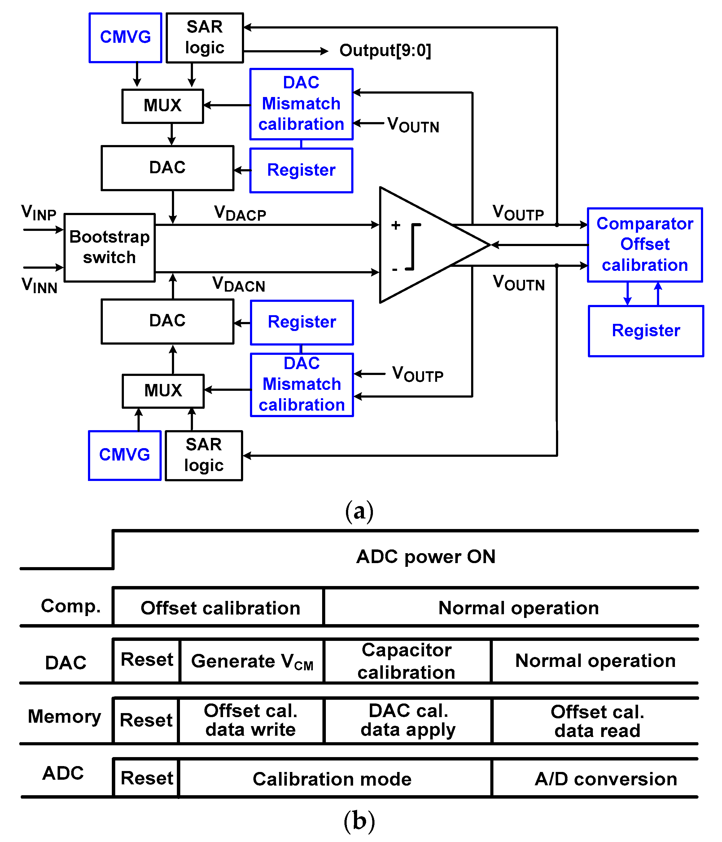
The proposed ADC supports a dual calibration technique for COC and DAC capacitor mismatch calibration. During the COC, we note that the capacitive DAC is not used for analog-to-digital (A/D) conversion. To realize the calibration without using separate circuit blocks, the DAC is reused for implementing the common-mode voltage generators (CMVG). During COC, a multiplexer (MUX) array selects inputs from the CMVG for the DAC. During normal A/D conversion, the inputs from SAR logic are selected. The linearity of SAR ADC is affected by the mismatch in the capacitive DAC. Because high mismatch errors occur for the large capacitors, the DAC mismatch calibration is applied to upper CT[i] arrays. To realize the calibration in an energy and area-efficient manner, the lower CB[i] are not calibrated; they require sufficient intrinsic linearity. Otherwise, they set the upper limit on performance.
2.1. Dynamic Latched Comparator
The dynamic latched comparator is widely used to reduce power consumption [
16]. We consider three issues for the design of the comparator: (1) the clocked operation of the comparator disturbs the top plate of DAC by kick-back; (2) systematic and random device mismatch creates an offset voltage
Voffset; (3) during monotonic switching,
Voffset depends on the CM voltage
VCM.
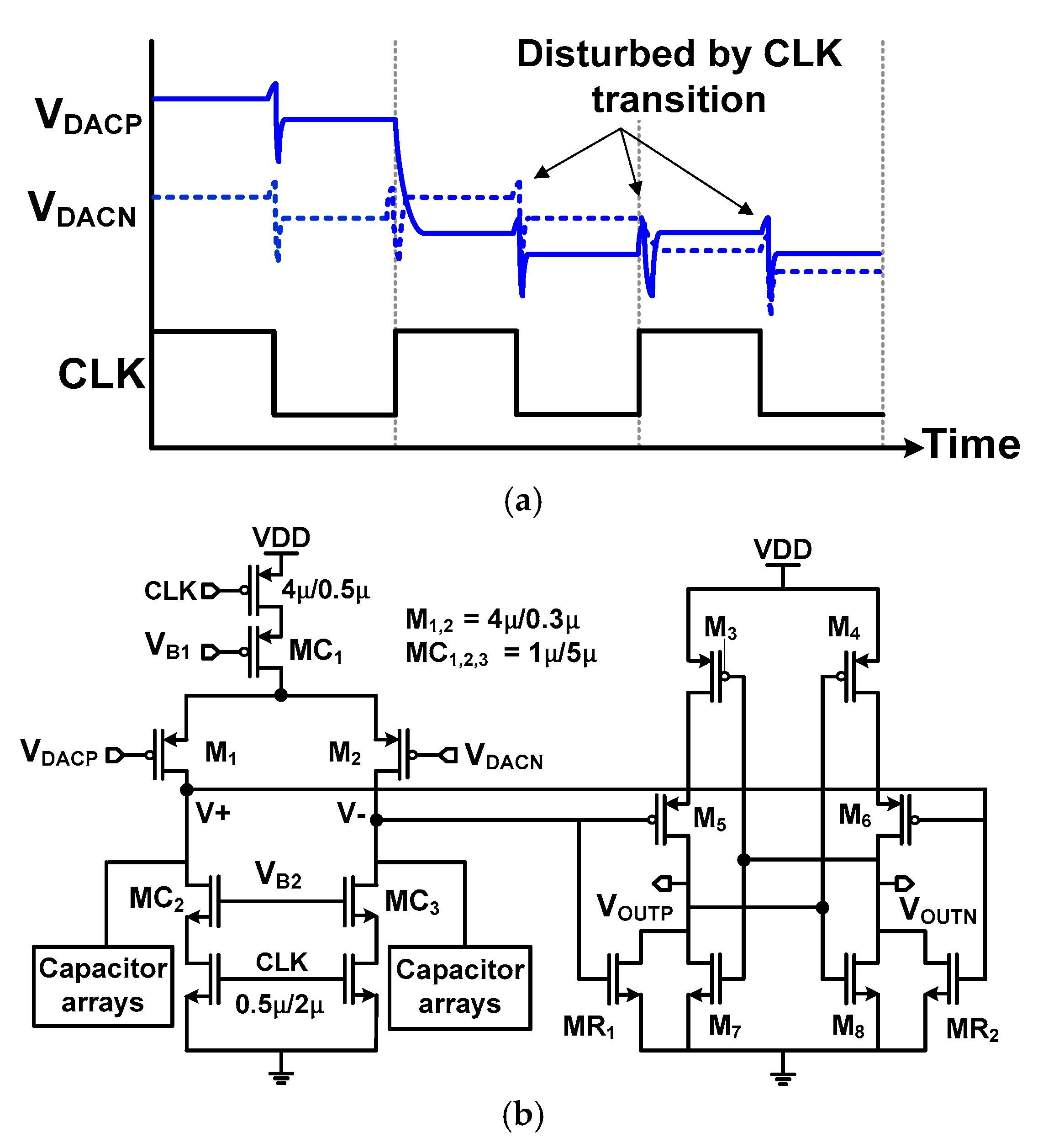
Figure 2a shows the waveforms of the DAC voltage
VDACP,N which are disturbed by the clock transition. In the dynamic latched comparator, the input difference is resolved when the clock signal CLK is switched from low to high. By the CLK transition, the kick-back noise is generated at the input of the comparator by clock feed-through [
17]. Then, there is a recovery period when
VDACP,N settles to a stable voltage. Because this is the time when the comparator starts resolving the input difference, a small asymmetry in this recovery period can cause a decision error.
Figure 2b shows a schematic of the comparator. By the use of auxiliary transistors (MR
1 and MR
2), hysteresis can exist in the comparator by the mismatch introduced through the process variations. Therefore, we use the common-centroid layout carefully to suppress the hysteresis. In addition, the comparator is carefully designed for kick-back suppression and CM-dependent offset calibration. To reduce the kick-back, the input transistor pair M
1,2 is shielded using three cascode transistors MC
1–3. To increase the output resistance of the MC
1–3, we choose a small aspect ratio of (W/L) = 1 μm/5 μm so that they operate in the saturation region. By the increased output resistance, the large voltage step created by CLK transition is attenuated as it goes through the MC
1–3 [
18]. The size and bias voltages for the cascode are chosen by circuit simulations. By adjusting the bias voltage
VB2, we are able to control the current through MC
2,3. When
VB2 is decreased from 1.2 to 0.7 V with
VB1 = 1 V, it effectively reduces the peak current through MC
2,3 from 7 to 1 μA during the CLK transition. In addition, we perform sizing optimization of M
1,2 from W/L = 8 μm/0.5 μm to 4 μm/0.3 μm. By the use of cascode and the size optimization, the peak value of kick-back is reduced from 4 to 1 mV. Although the small-size input pair and the cascode reduce the comparator speed, the proposed ADC is targeted for low-speed sensing applications. Therefore, the tradeoff does not greatly affect the overall performance of the ADC.
To handle
Voffset, the comparator is calibrated using a binary-weighted capacitor array. Because analog offset calibration requires additional DAC [
7], we choose a simple digital approach. Using a register array to store the offset calibration data, CM-dependent offset calibration is performed (See Section B for implementation detail.)
The
Voffset of the comparator consists of static (the first term) and dynamic (the second term) offsets, which can be written as
where Δ
VTH1,2 is the threshold mismatch,
VTH1,2 is the threshold voltage, Δ(W/L)
1,2 is the physical dimension mismatch between M
1 and M
2, and Δ
Rload is the load resistance mismatch [
3]. The dynamic offset is attributed to charge injection, thus voltage dependent.
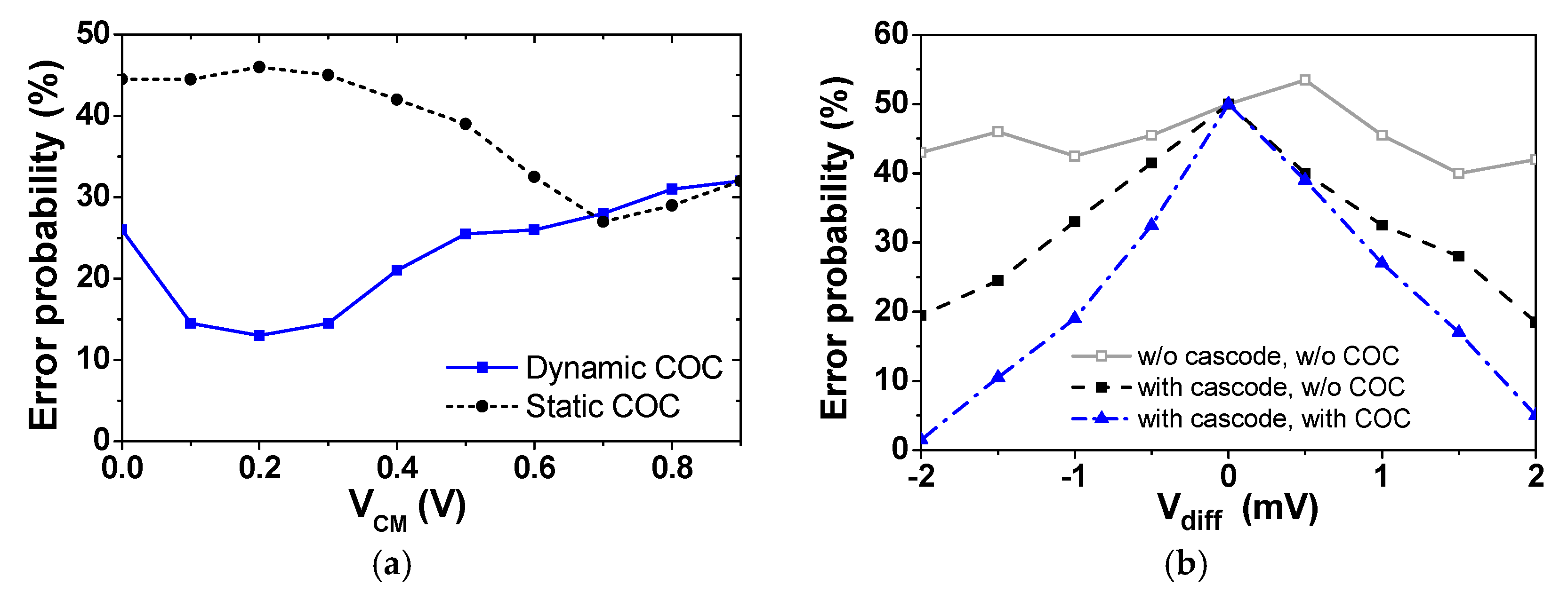
Figure 3a compares error probabilities obtained by static and dynamic offset calibrations. The result is obtained using Spectre transient noise simulation with the difference
Vdiff = 1 mV applied to the input of the comparator. The sampling rate is
fs = 4 kS/s and the supply voltage is
VDD = 1.8 V. The error probability is obtained by counting the case when the comparator makes the wrong decision out of 1000 simulations. The wrong decision is caused by the noise and the
Voffset of the comparator. Because the static approach performs the COC one time at
VCM = 0.9 V, it reduces the static offset only. The dynamic approach performs the COC at each
VCM from 0.9 to 0 V with a 112.5 mV step. And this approach reduces both the static and dynamic offsets. The result shows that the two approaches achieve a similar error probability at
VCM = 0.9 V. In the low
VCM range, however, the error of dynamic COC is significantly lower than that of static COC.
In addition, we evaluate the error probabilities as a function of
Vdiff.
Figure 3b shows the error probability of three comparators. The result is obtained by performing 1000 Monte Carlo simulations that consider both local and global process variation under a TTT corner. The result confirms that the error is significantly reduced when both cascode and COC are used. In the next section, we describe the implementation details for realizing dynamic COC.
2.2. Comparator Offset Calibration
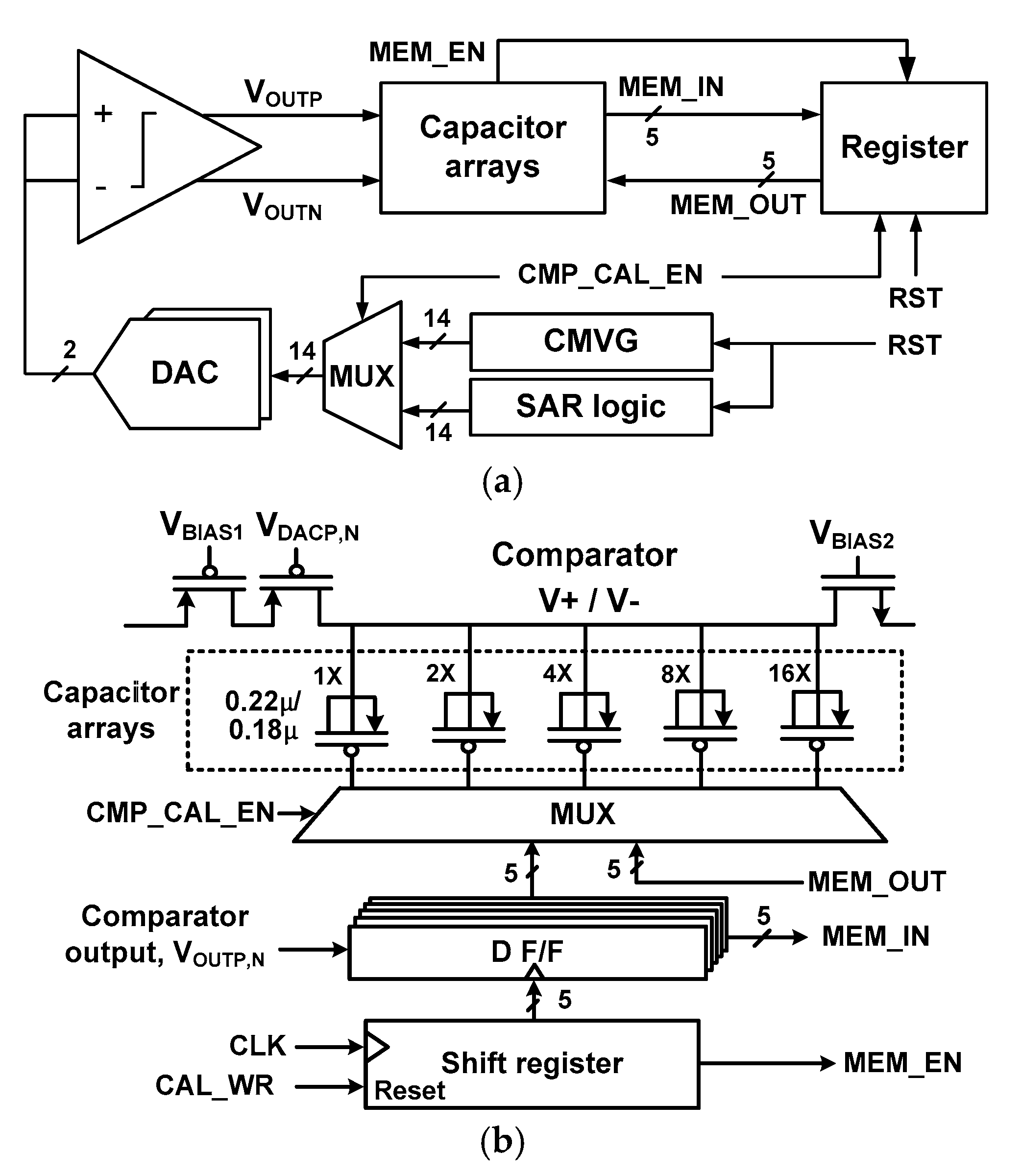
Figure 4a shows a block diagram to implement the dynamic COC. A reset signal RST initializes the digital logic and registers. A MUX controlled by CMP_CAL_EN selects the input to the DAC. When COC is enabled by CMP_CAL_EN = 1, the output from the CMVG is supplied to the DAC. For normal A/D conversion, the output from the SAR logic is input to the DAC.
Figure 4b shows the control block for the binary-weighted capacitor array. The residual offset is in theory reduced by half when increasing the number of calibration bits by one [
19]. We determine the number of array elements using circuit simulations. The error probability is reduced by 18.5% and 39.5% when the number of elements is increased to two and five, respectively. Considering the tradeoff between the complexity and the error, we choose 5-bit for the capacitor array elements. The manufacturer’s process specification provides statistical data for the mismatch of the threshold voltage, drain current, and the transconductance as a function of device size ratio (W/L)
0.5. By using the mismatch data corresponding to the size of the input pair M
1,2 into (1), we determine a typical
Voffset = 25 mV for the comparator. The proposed offset calibration method allows an offset correction up to ±24 least significant bits (LSB) in the 0.7 LSB step under TTT corner. Although the process corner changes the calibration range up to 20%, the 5-bit calibration scheme still covers the
Voffset range. In addition, the delay of the comparator does not vary significantly with the calibration code. When the mismatch in the DAC capacitor is not considered, it varies from 9 (FFF corner) to 13 ns (SSS corner) with
Vdiff = 0.
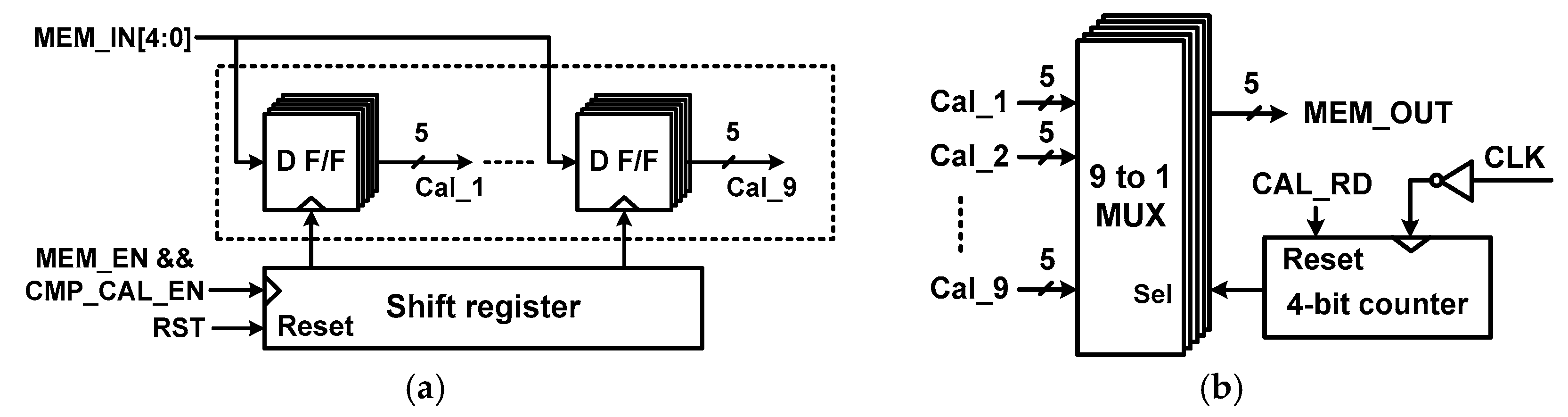
With the same VCM applied to the inputs of the comparator, the state of the capacitor is determined in order of weight by VOUTP,N. In the case of VOUTP = 1 (VOUTN = 1), it increases the capacitance at V+ (V−) node. This process is repeated five times. For each VCM step, this timing control is performed by the shift register, which is controlled by CAL_WR. The rising edge of CAL_WR clears the D F/F, which holds the previous data for the capacitor array. When the state of 5-bits is determined for a given VCM, MEM_EN is generated from the last stage of the shift register, which writes the calibration data to the register via MEM_IN[4:0]. This operation repeats until all nine VCM steps are processed. During normal A/D conversion, the stored data in the register are sequentially read using MEM_OUT[4:0], which sets the state of the capacitor array.
Figure 5 shows the schematic of the CMVG. The CMVG is implemented without using separate circuit blocks by reusing the DAC. To be compatible with monotonic switching where
VCM is gradually reduced, the CMVG generates nine
VCM steps of each 112.5 mV in the range from 0.9 to 0 V. Each
VCM is generated by controlling the bottom plate of the capacitor arrays C
T[6:0] and C
B[6:0]. With a reference voltage of 1.8 V, a
VCM step of 112.5 mV corresponds to 32
CU (
CU = 31.7 fF is a unit capacitor). To complete one cycle of COC, eight clocks are needed; one clock for reset, five clocks for determining the state of the capacitor array, and two clocks for the data store. Therefore, we use a CLK/8 divider for the CMVG. The
VDACP,N changes its value at every rising edge of CLK/8.
Figure 6a shows the block diagram of the register control for writing the calibration data Cal_j[4:0] (j = 1 to 9). When CMP_CAL_EN = 1 and MEM_EN = 1, the output of the shifter register provides the clock for D F/F. Then, MEM_IN[4:0] are written to the register with the rising edge of MEM_EN. During normal A/D conversion, the calibration data stored in the register are sequentially read out using a 9 to 1 MUX and a 4-bit counter as shown in
Figure 6b. The calibration data read signal CAL_RD resets a 4-bit counter and starts reading Cal_j[4:0] with every falling edge of CLK.
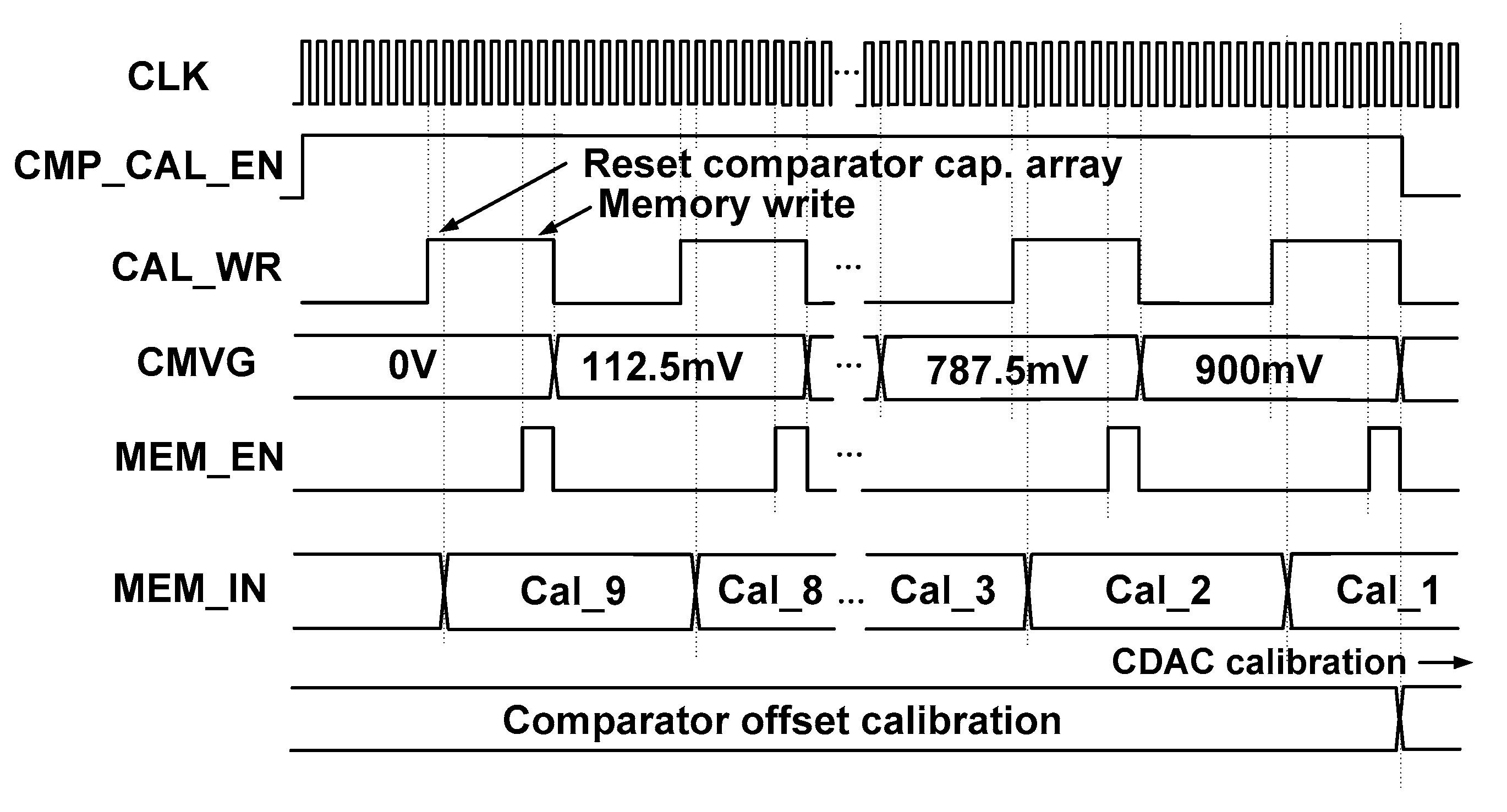
Figure 7 shows the timing waveform for the comparator offset measurement, which starts with CMP_CAL_EN = 1. For each
VCM step, the rising edge of CAL_WR is used for reset. During the period when CAL_WR = 1, the CMVG generates a
VCM to determine the state of the capacitor array. Then, the calibration data MEM_IN[4:0] are stored with the MEM_EN signal. When offset measurement for nine
VCM is finished, CMP_CAL_EN signal becomes low, which indicates the end of comparator offset measurement.
2.3. Digital-to-Analo Converter Capacitor Mismatch Calibration
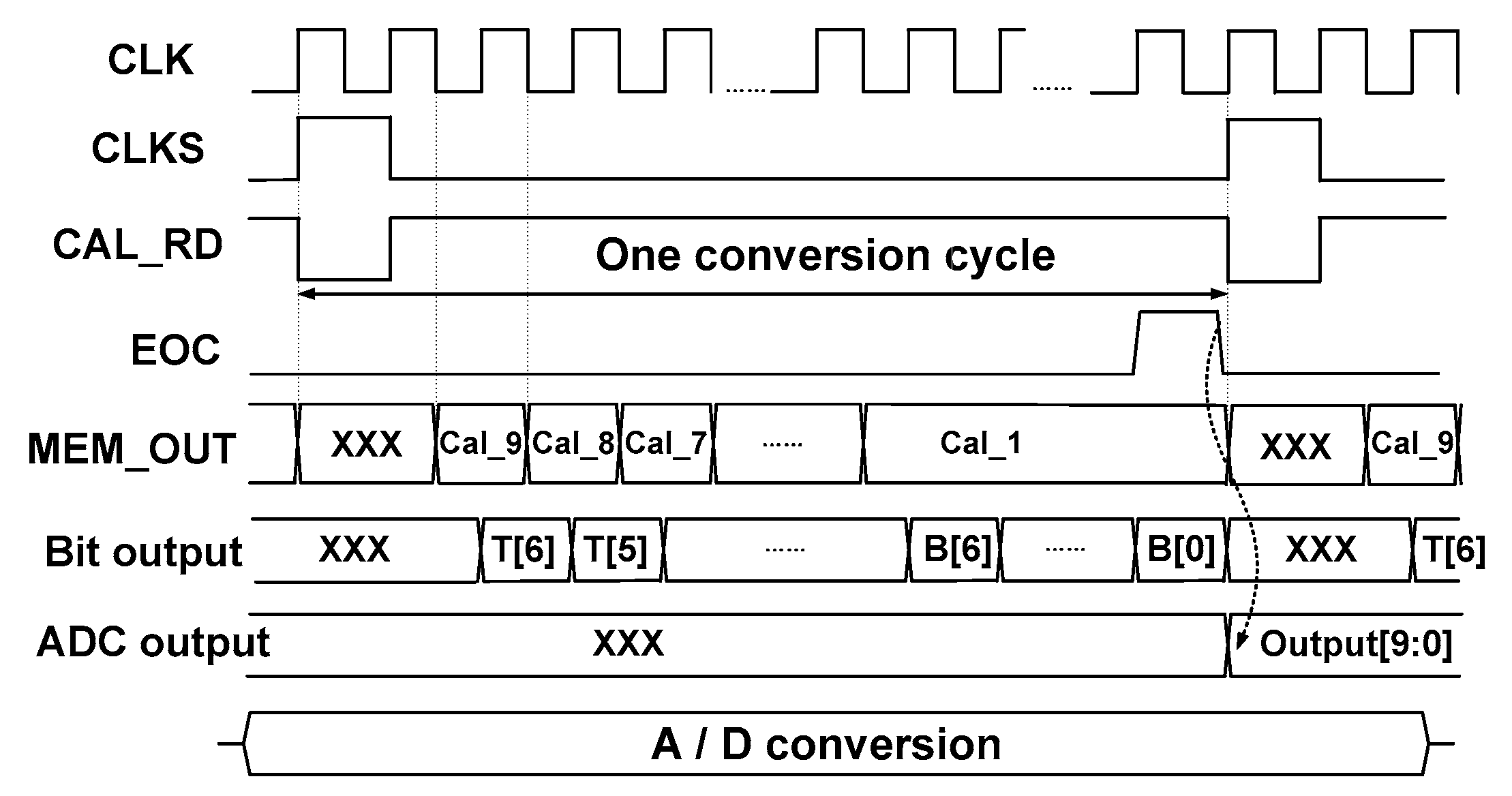
Figure 8 shows the timing waveform during the normal A/D conversion when the COC is applied. Before the comparator makes a decision, the calibration data MEM_OUT [4:0] are applied to the comparator. When CLK_RD becomes high, MEM_OUT [4:0] are read, which sets the state of the capacitor array in the comparator. When the comparator makes a decision, thermometer-coded bits T[6:0] and binary-coded bits B[6:0] are sequentially generated. When the B[6:0] switches,
VCM is already close to the ground and does not change significantly. Therefore, Cal_1[4:0] is used during this period. With the end-of-conversion (EOC), the ADC generates outputs.
Figure 9 shows the sequence of the calibration for detecting the DAC capacitor mismatch. The DAC array consists of C
T[i] and C
B[i]. We note that the one-bit of C
T[i] has a weight of 64
CU. Under the ideal matching condition, the sum of binary capacitors from C
B[6] to C
B[0] has the same weight, 64
CU. For the DAC capacitor mismatch calibration, we detect the difference between
VDACP and
VDACN, which can be used to evaluate the mismatch between the upper and lower DAC. The proposed approach is different from the previous works [
7,
8,
11], which evaluate the mismatch using the DAC in the same branch. Although the previous approach can potentially achieve a better calibration result, it requires a rather complicated calibration logic as well as additional calibration DAC. By reusing the offset-calibrated comparator, our approach evaluates the mismatch in the DAC capacitor without a separate circuit block. A small mismatch in the DAC capacitor leads to a slight difference between
VDACP and
VDACN, which leads to a large comparator delay for generating output. In the case of a large mismatch, the comparator generates output with a relatively short delay. The delay is encoded using two-bit data for each C
T[i]. Due to circuit complexity, C
B[i] is not calibrated.
Using the symmetric properties of the differential structure, the proposed calibration method measures the mismatch between the upper and lower DAC. The mismatch in the one-bit CT[i] is sequentially detected by using the sum of CB[i] in the other branch. The positive DAC branch is evaluated first and the negative DAC branch is calibrated next. The procedure can be summarized as follows:
- (1)
Before starting mismatch calibration, the bottom nodes of all capacitors in the DAC are reset by connecting them to the ground.
- (2)
To evaluate the mismatch error of CT[0], connect the bottom plate of CT[0] in the positive branch to the reference voltage VREF and generate VDACP. Then, connect the bottom plate of all CB[6:0] in the negative branch to VREF and generate VDACN. If there is a mismatch, the difference between VDACP and VDACN is reflected as the output delay in the comparator.
- (3)
The delay in the comparator is encoded using two-bit data LSB_P[1:0], which represents mismatch information for CT[0] in the positive branch.
- (4)
Sequentially evaluate the mismatch of the remaining thermometer-coded capacitors (CT[1] − CT[6]) in the positive DAC branch.
- (5)
In the same manner, evaluate the mismatch of seven CT[i] in the negative DAC branch. This mismatch information is encoded using two-bit data LSB_N[1:0].
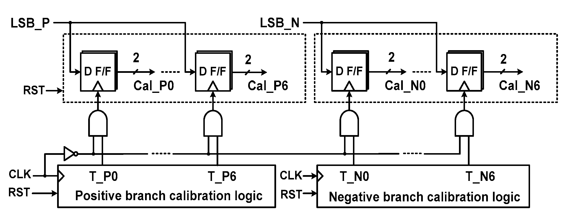
Figure 10 shows the block diagram for realizing the proposed DAC mismatch calibration. It consists of a DAC calibration logic, a delay detector, registers, and compensation capacitors. During mismatch calibration, CAL_END selects the MUX to receive the input from the DAC calibration logic. The calibration logic sequentially controls the bottom plate of capacitors in the positive and negative DACs. Then, the delay detector generates LSB_P[1:0], which indicates the mismatch data of the positive DAC (LSB_N[1:0] for the negative branch). The two-bit outputs are sequentially written seven times into the register. When the mismatch evaluation is finished for C
T[0:6], the mismatch data are retrieved from the register. There are seven register outputs for positive (Cal_P0[1:0]-Cal_P6[1:0]) and negative (Cal_N0[1:0]-Cal_N6[1:0]) branches. These outputs are used to set the compensation capacitors attached to each C
T[0:6].
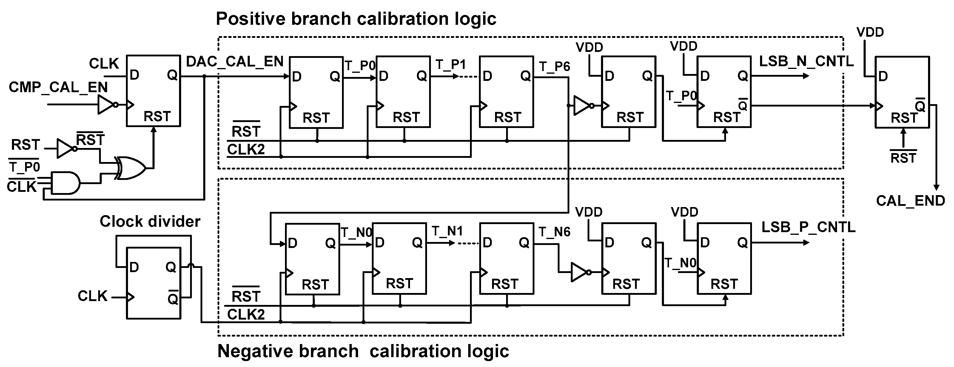
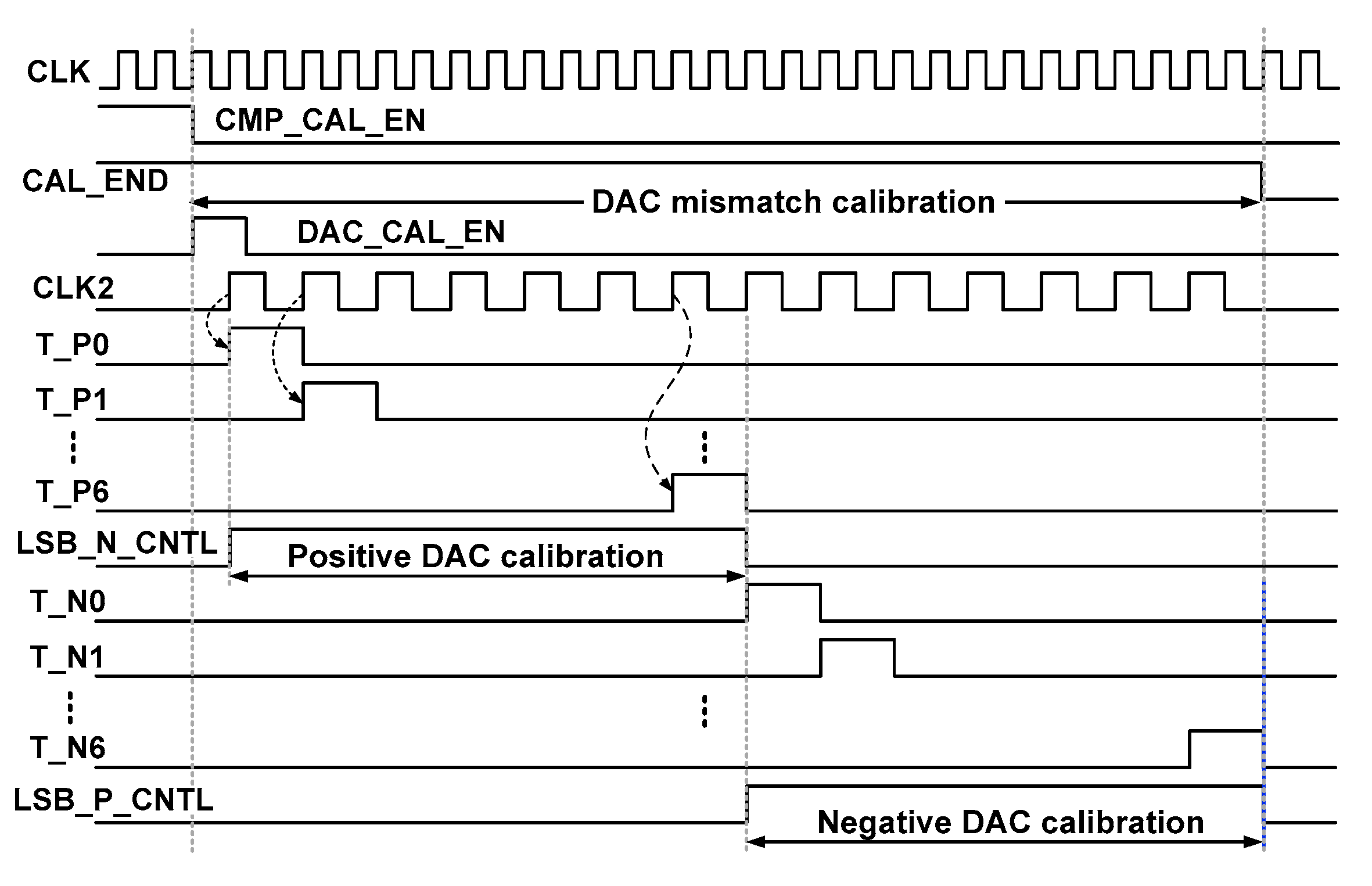
Figure 11 shows the schematic of DAC calibration logic. It consists of positive/negative branch calibration logic, a clock divider, and a logic gate. Comparator offset and DAC mismatch calibrations are enabled by signals CMP_CAL_EN and DAC_CAL_EN, respectively. The two calibration logics sequentially generate the signals to control the bottom plate of the capacitors in the DAC. To control the other side of the DAC, the period of positive (negative) DAC calibration is set by the LSB_N_CNTL (LSB_P_CNTL) signal. Two clock cycles are used for evaluating the comparator delay and writing the mismatch data to the register, which is generated by the clock divider. From the last stage of D F/F, CAL_END is generated, which indicates the end of the calibration phase.
Figure 12 shows the timing waveform of the DAC calibration logic. The low-level transition of the CMP_CAL_EN signal indicates the end of COC. Then, the DAC_CAL_EN signal is enabled to perform the DAC capacitor mismatch calibration and the shift registers in the positive branch calibration logic start operation. First, T_P0 becomes active to switch the bottom plate of capacitor C
T[0] in the positive branch. During this time, LSB_N_CNTL controls the bottom plate of capacitors C
B[6:0] in the negative branch. The LSB_N_CNTL is enabled until mismatch evaluations are performed for all C
T[0:6] in the positive DAC branch. The negative branch calibration logic operates in a similar manner using LSB_P_CNTL. When the DAC mismatch calibration is finished, CAL_END becomes low.
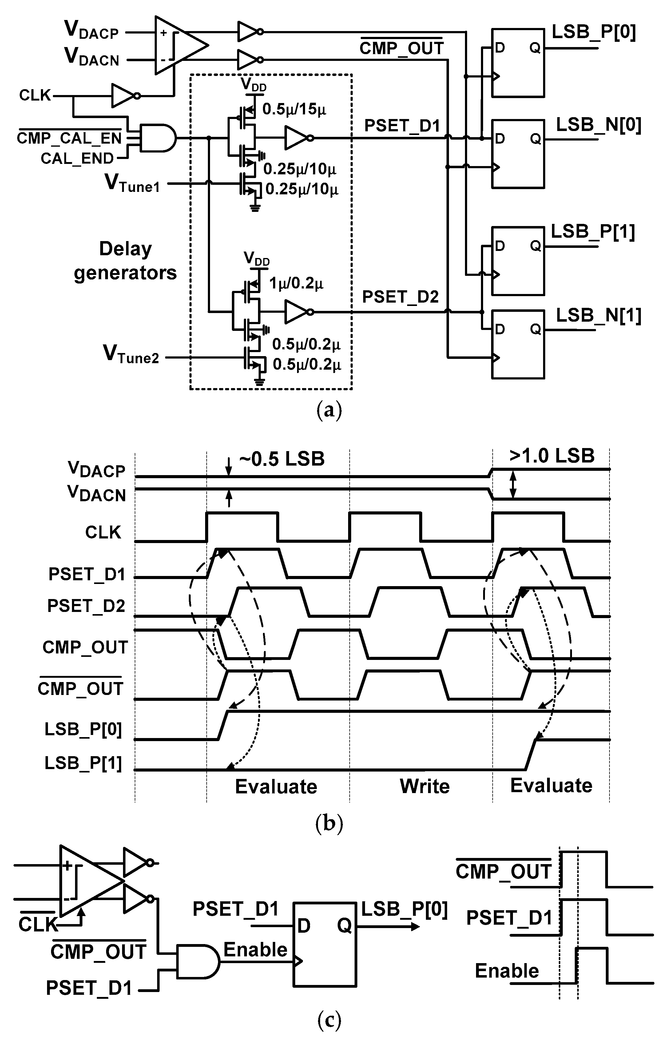
Figure 13a shows the schematic of the delay detector. The detector consists of two delay generators and D F/Fs. The outputs PSET_D1,D2 of the delay generator are used for the reference for detecting the mismatch. They are applied to the input terminal of D F/F. Then, the sampling operation of PSET_D1,D2 is performed by the comparator output
. The sampling evaluates the amount of mismatch existing in the positive (negative) DAC branch using two-bit data LSB_P[1:0] (LSB_N[1:0]).
The comparator delay depends on the DAC capacitor mismatch. When the mismatch error of C
T[0] in the positive branch is evaluated (See
Figure 9), for example, the capacitors in the negative branch is assumed to have sufficient intrinsic linearity; we assume the total sum of these capacitors to be 64
CU even in the case when the individual capacitor C
B[i] experiences the worst-case mismatch deviation of 1% from the ideal binary ratio. To meet the requirement, we carefully lay out the routing paths and iteratively trim the size of each capacitor with the aid of a CAD tool. Instead of SAR logic, the DAC calibration logic controls the bottom nodes of capacitors. Then, the difference Δ
Vin between
VDACP and
VDACN is obtained [
2] using:
where ΔC
T[0] is the deviation from the ideal 64
CU. Similar expressions can be written for C
T[i]. The delay time
tD of the comparator can be written as the sum of two terms, the load capacitor discharge time
tcharge and the latch delay time
tlatch [
20] as:
where
VTH7,8 is the threshold voltage of the transistor M
7,8 (See
Figure 2b),
IBIAS2 is the bias current of the second stage,
CL,out is the output load capacitance,
CL,V+ is the capacitance at the output of the first stage,
gm,eff is the effective transconductance of the back-to-back inverter,
gmR1,2 is the transconductance of the intermediate stage transistors MR
1,2, and
gm1,2 is the transconductance of the input pair. The first term of (3) is independent of Δ
Vin but affected by the process corner. The second term is inversely proportional to Δ
Vin.
Using (2), we obtain ΔVin of 0.6 and 0.9 LSB for 1.0% and 1.5% capacitor mismatch. Considering some margin for the mismatch, the delay generator is sized to produce proper delay so that mismatch error from 0.5 to 1.5 LSB is detected. To prevent malfunction, we determine the proper delay in the comparator and the delay generator by performing extensive Monte-Carlo simulations. Because the delay in these circuits shares a global process corner, we are able to mitigate the mismatch between delay detectors by using careful layout.
Table 1 shows the delay depending on process corners. The result shows that the comparator delay is reduced when the process corner is changed from SSS to FFF corner as expected. Using the difference between the total delay and the delay without mismatch, we are able to extract the delay depending on the mismatch. Circuit simulations show that the delay has an approximate inverse linear relationship with the error Δ
Vin. Therefore, the delay threshold for PSET_D1,D2 is chosen by using three equal delay regions. To deal with the process variation, the delay is further tuned using
VTUNE1,2 in the delay generator.
Figure 13b shows the timing waveform where the mismatch is evaluated in the positive DAC branch. When the mismatch is small, the difference between
VDACP and
VDACN is also small, resulting in a relatively long delay in the comparator [
21]. For example, consider the case when the mismatch is more than 0.5 LSB but less than 1.0 LSB. In the evaluation phase,
rises after PSET_D1 which sets LSB_P[0] to high and LSB_P[1] to low. The LSB_P[0:1] is subsequently written to the register. When the delay detector samples the output of the comparator using D F/F, meta-stability can occur. To remove this, we insert a logic gate to generate an Enable signal as shown in
Figure 13c. In this way, the Enable signal provides the clocks for D F/F in a well-defined sequence and removes meta-stability.
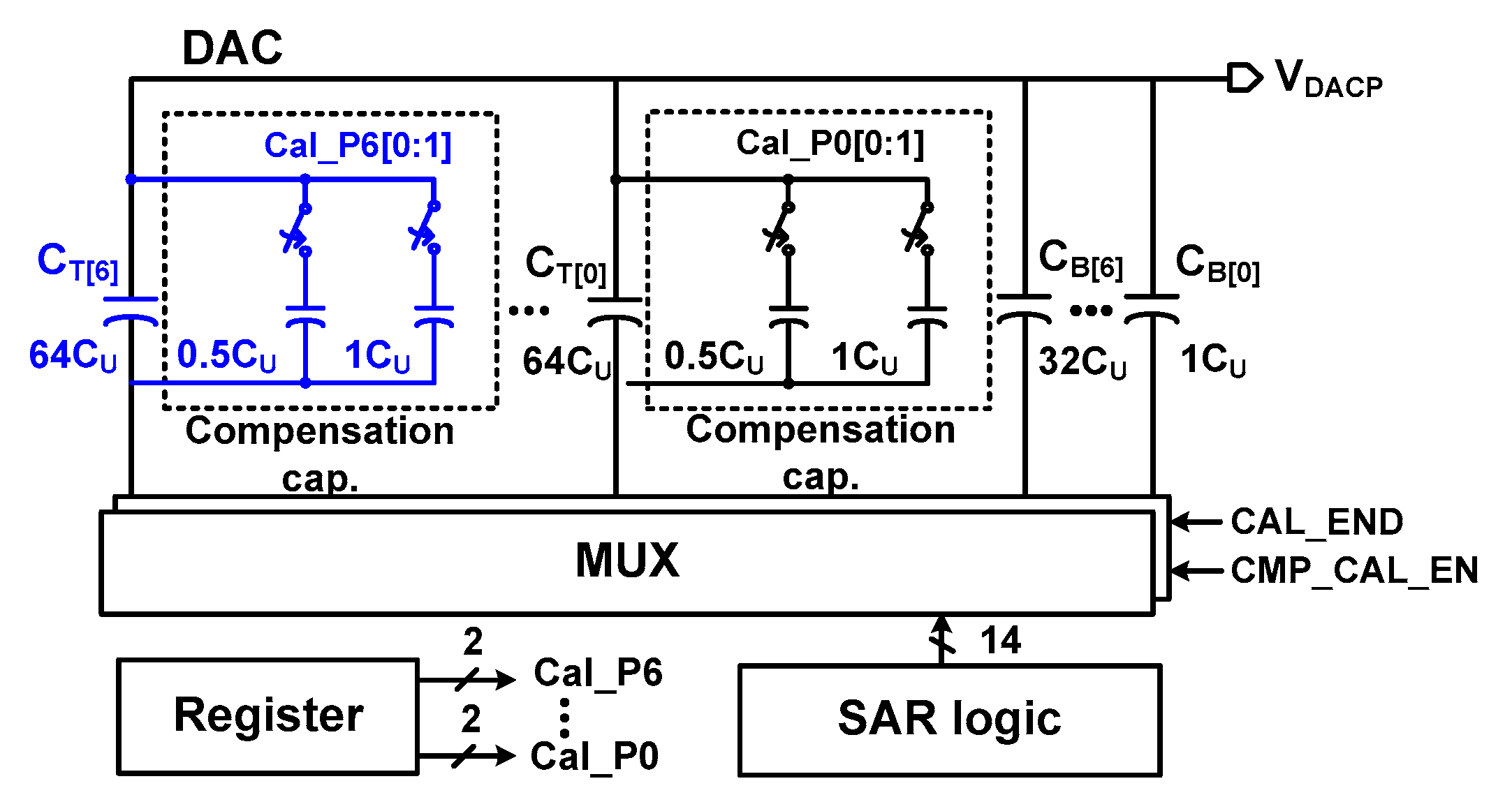
By the delay detector, two-bit data (LSB_P[1:0] and LSB_N[1:0]) for each C
T[0:6] in the two branches are generated. By the calibration logic, the data are sequentially written in the register (
Figure 14). The data are used to control the switch for the compensation capacitors attached to each C
T[0:6], as shown in
Figure 15. Each compensation capacitor consists of 0.5
CU and 1.0
CU. The value of the capacitors is chosen considering a worst-case mismatch (2%) of 64
CU. The effect of calibration can be enhanced by using both add and subtract operations. The subtract operation is implemented by taking advantage of the differential structure [
22]. To simplify the logic for the subtract operation and consider the layout parasitic, the size of the original DAC capacitors is reduced by 0.5
CU. Then, the error compensating range is from −0.5 to +1 LSB in the 0.5 LSB step.
In order to assess the performance improvement by the proposed calibration technique, behavioral simulations are performed using Matlab. By including random DAC capacitor mismatch in the behavioral model of the ADC, we perform 1000 Monte-Carlo simulations. Comparator and kT/C noises are not included. The foundry datasheet shows 1% capacitor mismatch which is a conservative estimate. Because there is additional mismatch caused by routing and fringing components, we consider the random mismatch from 1.0% to 2.5%.
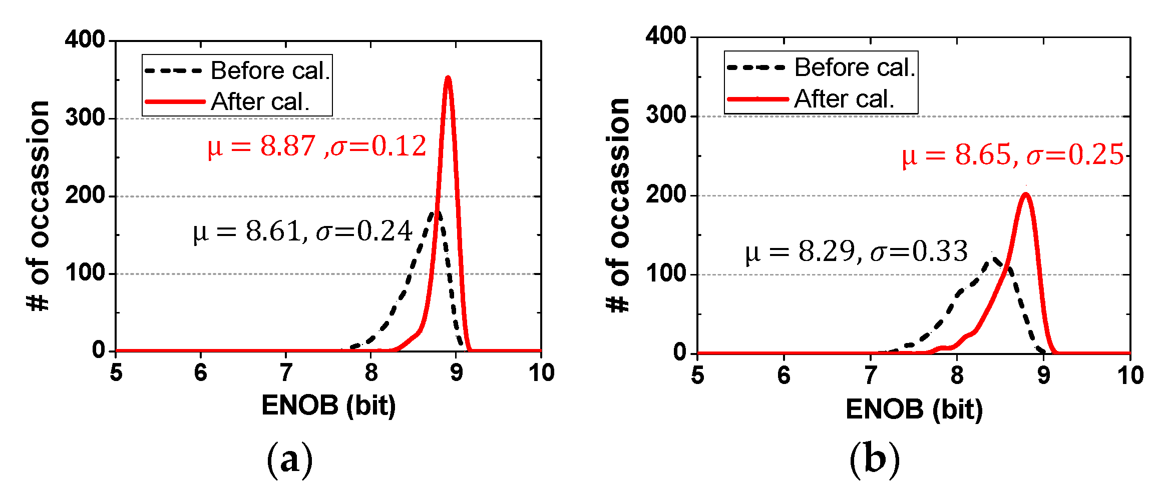
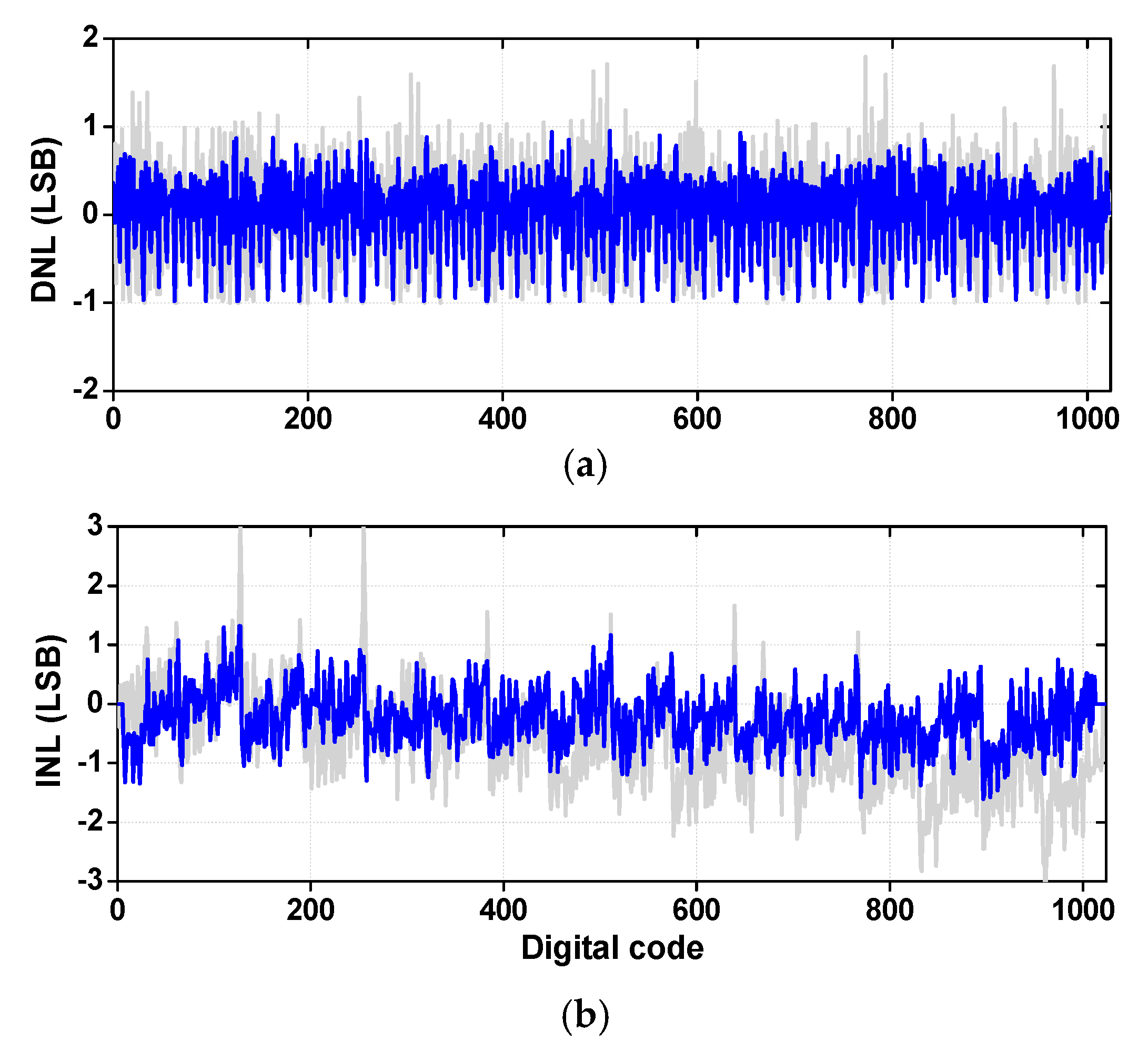
Figure 16 shows the probability distribution of an effective number of bits (ENOB) before and after the mismatch calibration. In the case of 1% mismatch, the average ENOB before and after calibration is 8.61 and 8.87 bits, respectively. The standard deviation is reduced from 0.24 to 0.12 bits by the calibration. In the case of 1.5% mismatch, the average ENOB improves from 8.29 to 8.65 bits. The standard deviation is reduced from 0.33 and 0.25 bits after calibration. The binary-weighted capacitors are not calibrated. With the quantization noise and the discrete value of compensation capacitors, these set the upper limit on performance after calibration. In the case when the binary capacitors are calibrated, the ENOB improves by 0.3–0.4 bits depending on the mismatch. In addition, we perform simulations for static nonlinearity. For 2% mismatch, the peak DNL is +0.09/−0.63 LSB before calibration and it is reduced to +0.08/−0.32 LSB after calibration. The peak integral non-linearity (INL) is +1.71/−1.72 LSB before calibration and it is improved to +0.74/−0.75 LSB after calibration. The result shows that the proposed DAC mismatch calibration is effective at improving both dynamic and static performances of the ADC.
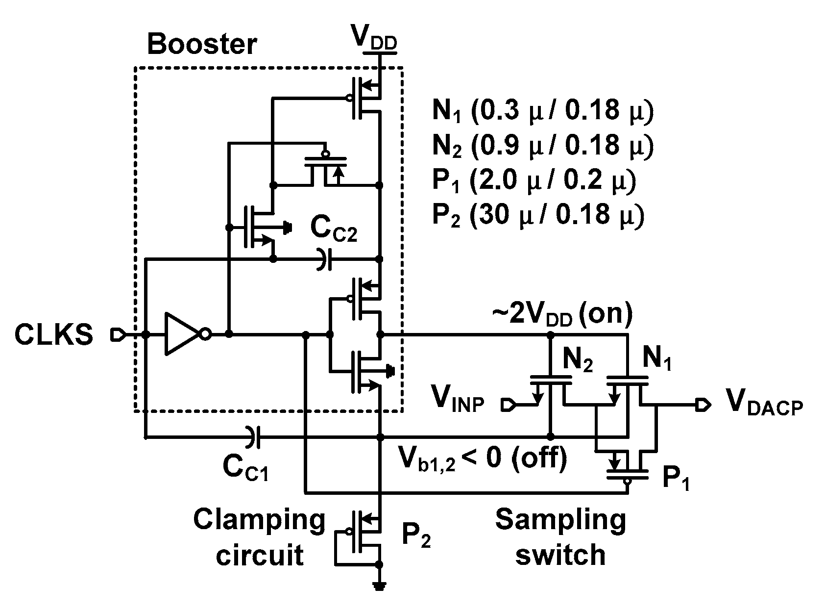
2.4. Bootstrap Sampling Switch
Figure 17 shows the proposed bootstrap sampling switch. Based on the previous work [
23], it is modified to reduce leakage-induced error (off-state) and sampling error (on-state). It consists of a booster, a sampling switch, and a clamping circuit.
The sampling error defined by the difference between VDACP and VINP occurs due to the on-resistance of the switch. To reduce the resistance, a boosted voltage of about 2VDD is applied to the gate of N1 and N2 through the capacitor CC2. In addition, P1 in parallel with N1 forms a transmission-gate which further reduces the on-resistance. To reduce the leakage-induced error, the threshold voltages of N1 and N2 (both are inside deep n-well) are increased by controlling the body terminal. When the sampling clock CLKS is high, the body voltage Vb1,2 is set to the threshold voltage of P2 by the clamping circuit. When CLKS goes low, Vb1,2 is reduced by VDD through the capacitor CC1, which is about −1.3 V. The size of these transistors is optimized by considering the tradeoff between the on-resistance and leakage-induced error.
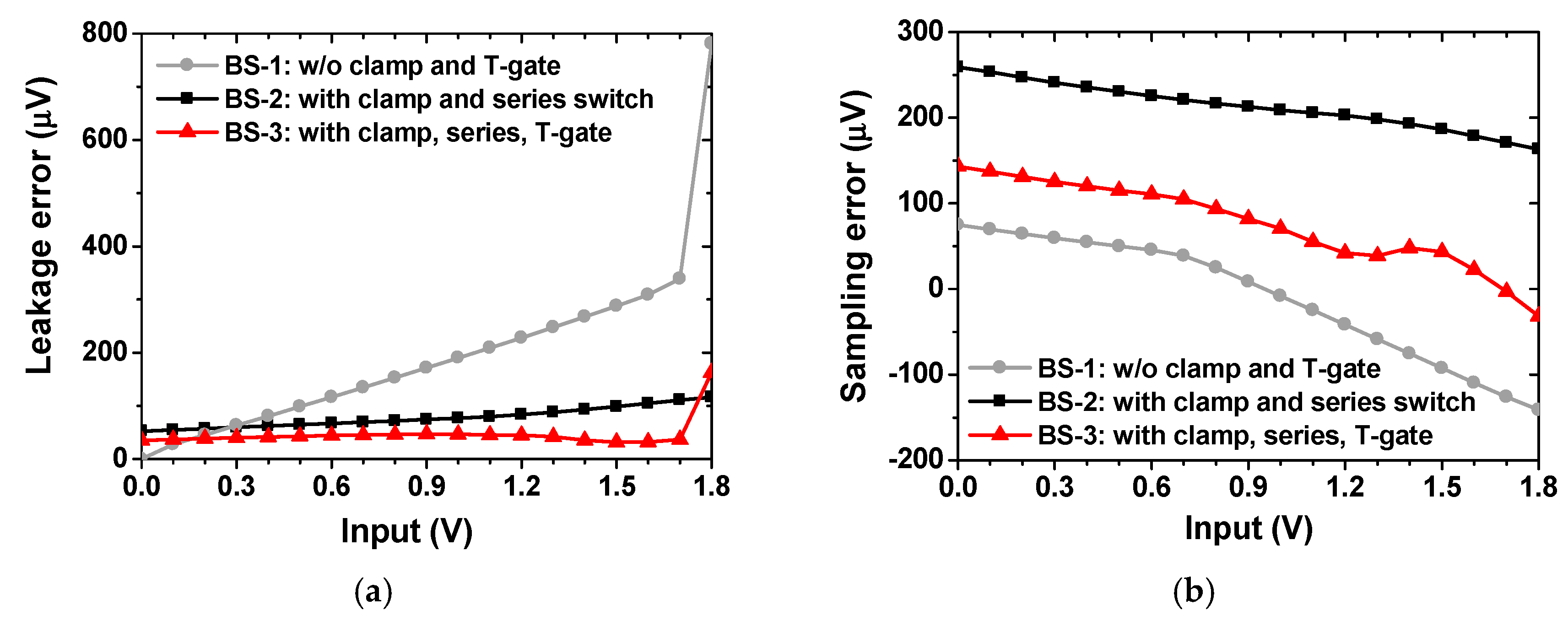
Figure 18a compares the leakage-induced error as a function of
VINP. The result is obtained from post-layout simulations with a sampling rate of 3 kS/s. The
VDACP is measured at 1 ms after the input
VINP is sampled. Three cases of the bootstrap switch (BS) are shown; (1) BS-1 having transmission-gate without a clamping circuit; (2) BS-2 having a clamping circuit and the series switch (N
1 and N
2) only [
23]; (3) BS-3 having a clamping circuit and the transmission-gate (
Figure 17). In the case of BS-1, the leakage-induced error increases with
VINP reaching 800 μV at
VINP = 1.8 V. The result shows that BS-3 has a smaller error than that of BS-2 except at
VINP = 1.8 V; BS-3 shows a leakage-induced error less than 50 μV up to
VINP = 1.7 V. The worst-case error is 180 μV.
Figure 18b shows the sampling error as a function of
VINP. The turn-on voltage of the sampling switch is 2V
DD. The gate-to-source voltage
Vgs of the switch, thus, the turn-on resistance depends on
VINP. This causes the sampling error to vary with the input. A constant
Vgs bootstrapping technique is reported [
24]; it can be challenging to implement this technique under different process corners. Another work focuses on reducing the turn-on resistance only [
25]; this approach can suffer from the leakage error when operated at a low sampling rate. The result shows that the BS-3 shows overall smaller error than that of BS-2; the sampling error is reduced by using a transmission-gate. BS-3 shows a worst-case sampling error of 150 μV, which is higher than that of BS-1. However, the high leakage-induced error of BS-1 is not suitable for our application.


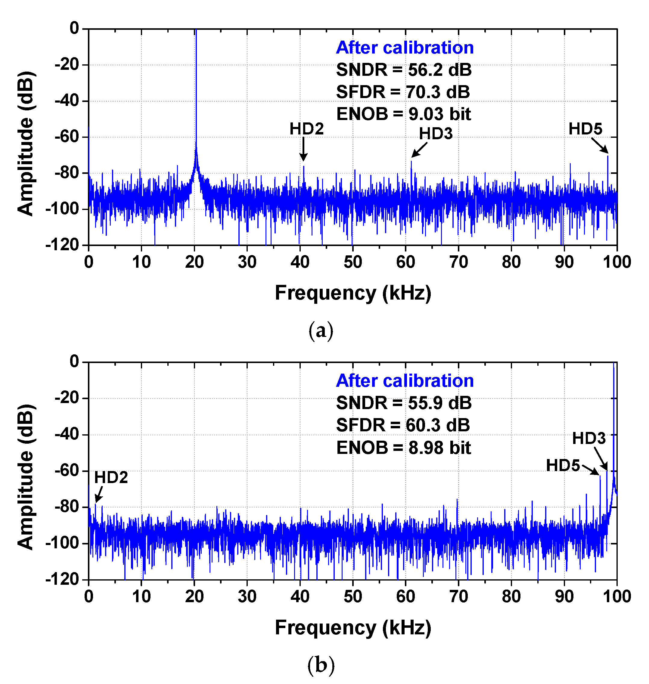
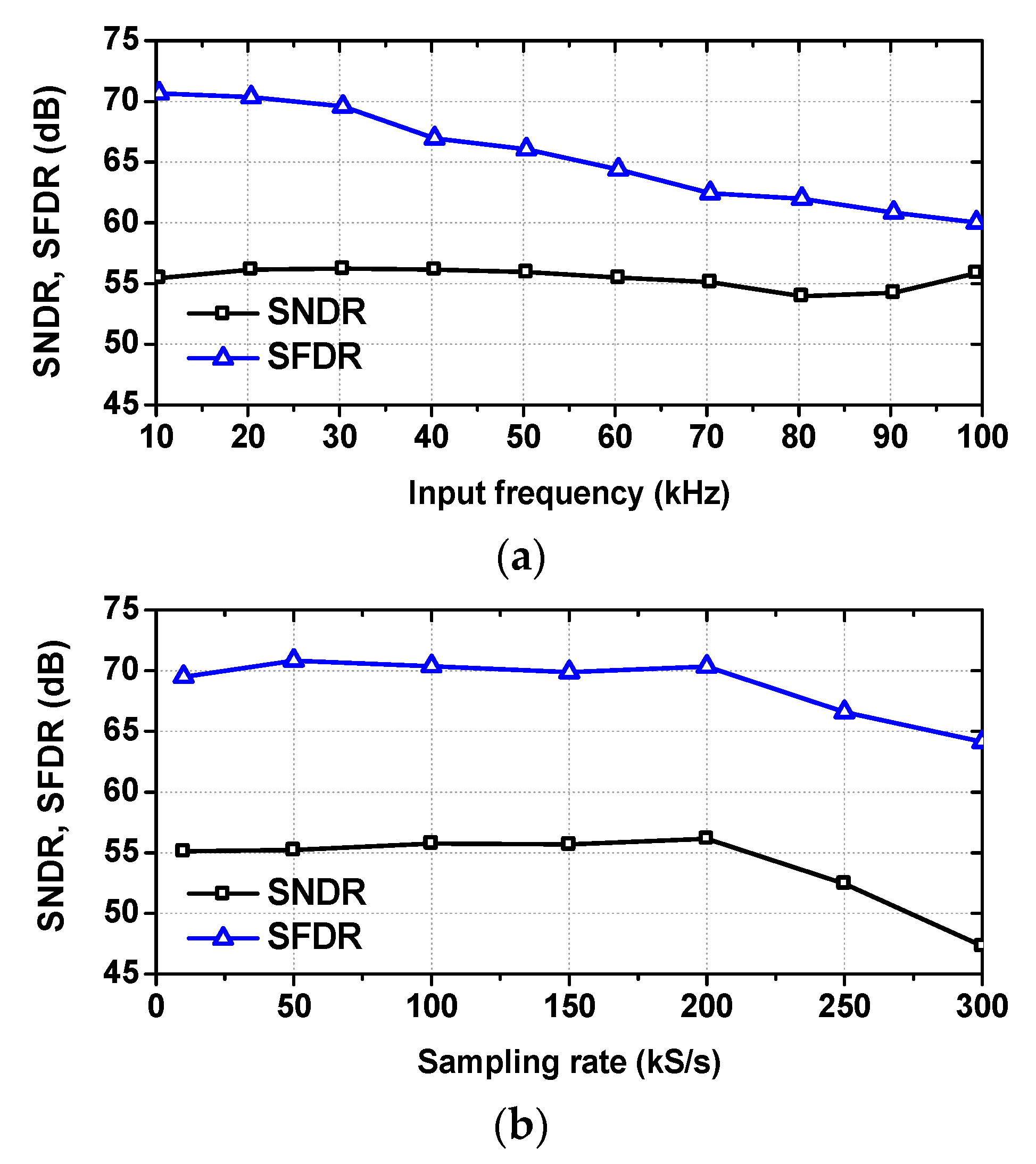
