Article

Modeling and Experimental Analysis on the Temperature Response of AlN-Film Based SAWRs

1
Department of Precision Instrument, Tsinghua University, Beijing 100084, China
2
State Key Laboratory of Precision Measurement Technology and Instruments, Tsinghua University, Beijing 100084, China
*
Author to whom correspondence should be addressed.
Sensors 2016, 16(8), 1205; https://doi.org/10.3390/s16081205
Submission received: 12 June 2016 / Revised: 25 July 2016 / Accepted: 26 July 2016 / Published: 30 July 2016
(This article belongs to the Section Physical Sensors)

Abstract

:
The temperature responses of aluminum nitride (AlN) based surface acoustic wave resonator (SAWR) are modeled and tested. The modeling of the electrical performance is based on a modified equivalent circuit model introduced in this work. For SAWR consisting of piezoelectric film and semiconducting substrate, parasitic parameters from the substrate is taken into consideration for the modeling. By utilizing the modified model, the high temperature electrical performance of the AlN/Si and AlN/6H-SiC based SAWRs can be predicted, indicating that a substrate with a wider band gap will lead to a more stable high temperature behavior, which is further confirmed experimentally by high temperature testing from 300 K to 725 K with SAWRs having a wavelength of 12 μm. Temperature responses of SAWR’s center frequency are also calculated and tested, with experimental temperature coefficient factors (TCF) of center frequency being −29 ppm/K and −26 ppm/K for the AlN/Si and AlN/6H-SiC based SAWRs, which are close to the predicted values.

1. Introduction

Surface acoustic wave resonators (SAWR) are widely used in sensing and telecommunicating industries [1,2,3,4]. Most of the conventional SAWR devices are based on bulk piezoelectric materials such as quartz, LiNbO3, and LiTaO3, but the decomposition or the weakening of piezoelectricity limits their working temperature within a relatively low range [5,6], thus novel piezoelectric materials with good thermal stabilities are valuable for high temperature applications. Several literatures have summarized that novel piezoelectric materials such as langasite, GaPO4, and YCa4O(BO3)3·(or YCOB) [5,7] are promising for high temperature environment. However, the majority of them are bulk materials which are less conventional and more expensive than film-like materials.
Aluminum nitride (AlN), is a non-ferroelectric piezoelectric material with a high melting point, high thermal conductivity [7,8], being compatible with most commonly seen CMOS fabrication processes [9,10,11]. Besides, AlN can be deposited on commercialized substrates such as Silicon (Si), hexagonal Silicon Carbide (α-SiC), poly-crystalline cubic Silicon Carbide, diamond and sapphire [12,13,14,15,16]. Among these aforementioned substrates, Si and α-SiC are probably the most compatible ones with conventional micro-fabrication processes. Therefore it is of interest to study the temperature responses of SAWRs based on AlN/Si and AlN/α-SiC in respect of the electrical property and center frequency.
In previous literatures, the equivalent circuit model of SAWR (Figure 1) has been developed and used to predict the electrical performance of SAWR [17,18,19]. As can be seen, the equivalent circuit of SAWR consists of the equivalent circuit components representing the inter-digital transducer (IDT) part, the reflectors on both sides (ZR), the transmission lines between IDT and reflectors (Zt), and the port connected with IDT, among which, the equivalent circuit of the IDT part is established to describe the electro-mechanical coupling between the alternating current (AC) signal and SAW.
For the AlN/Si and AlN/α-SiC based SAWRs in this work, the IDT parts of the devices which are connected with the electrical port will be affected by the parasitic parameters from the semiconducting substrate (Si, 6H-SiC as one of α-SiC’s poly-types in this work), hence the aforementioned classic equivalent circuit shall be modified to take this effect into consideration. This work introduces the modification of the equivalent circuit model by analyzing the origins of the parasitic parameters and their equivalent electrical components. The modified equivalent circuit model is further used for calculating the electrical performance of the AlN film based SAWRs.
The temperature coefficient factor (TCF) of SAWR’s center frequency is another important aspect of temperature responses. In this work, the TCF of each composing material (AlN, Si, and 6H-SiC) is calculated for a prediction of SAWR’s TCF, and the influence from the thermal mismatch between AlN and the substrate is analyzed.

2. Modeling

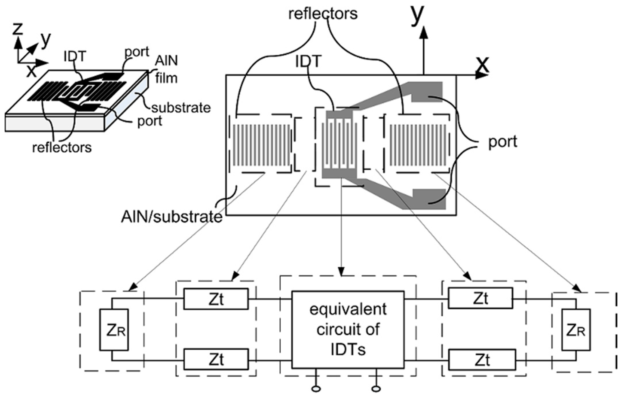
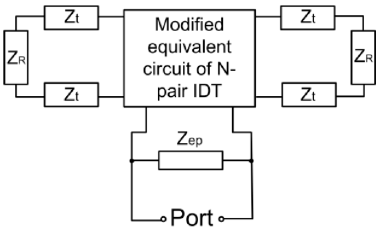
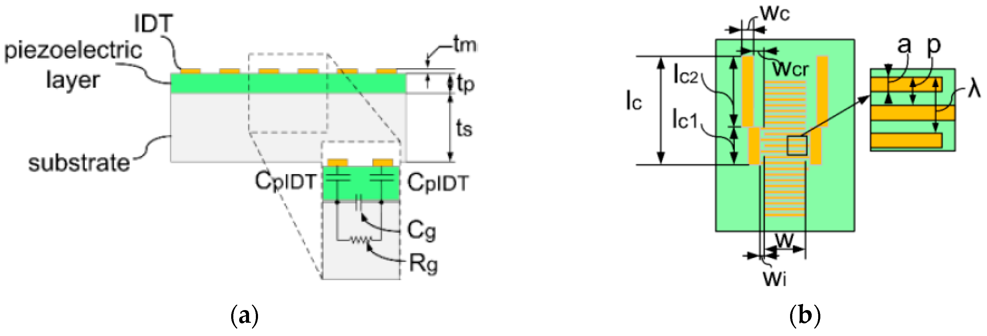
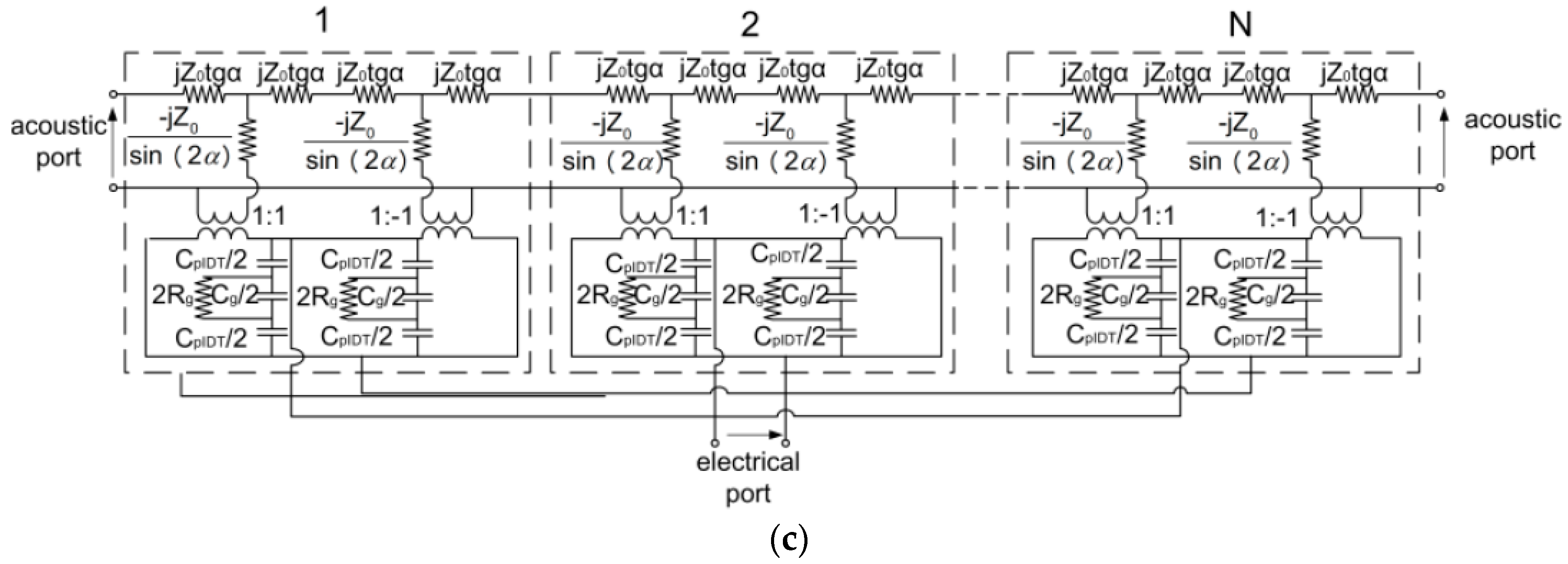
2.1. Modification of the Equivalent Circuit of IDT

With the existence of the aforementioned parasitic parameters from the semiconducting substrate, the equivalent electrical components between IDT grids are modified, as shown in Figure 2a, where CpIDT represents the capacitor of the piezoelectric layer under the IDT electrodes, Rg represents the resistor from the substrate at the gap between the IDT electrodes, and Cg represents the capacitor from the substrate and piezoelectric layer at the same area.
Thus the equivalent circuit model of the IDT part can be derived by combining the equivalent circuits of single pair IDT, as shown in Figure 2c. The acoustic ports of single IDT are connected in serial and the electrical ports are connected in parallel. With the geometric definitions of the SAWR in Figure 2b, the equivalent circuit components can be given as:
R g = R ( p a ) w
C g = ε 0 ε p wt p p a + ε 0 ε s , c wt s p a
C pIDT = ε 0 ε p aw t p
where R is the square resistance of the substrate, tp is the thickness of the piezoelectric layer, ts is the thickness of the substrate, εs,c and εp are the complex relative permittivity of the substrate and the piezoelectric layer, respectively. Z0 is the equivalent electrical impedance representing the acoustic impedance from the piezoelectric layer and the substrate, and has been given by [20] as:
Z 0 = 2 π ω 0 C s K 2
where ω0 is the angular resonant frequency of SAWR, Cs is the static capacitor storing the electrical energy between the IDT electrodes, and can be given by Equation (5), where Cg,r is the real part of Cg:
C s = ( 2 C pIDT 1 + C g , r 1 ) 1
K2 is the electrical-mechanical coupling coefficient of the piezoelectric material, and can be derived experimentally through the serial and parallel resonant frequencies (fs and fp, respectively) of the SAWR [21,22]:
K 2 = ( π f s / 2 f p ) cot ( π f s / 2 f p )

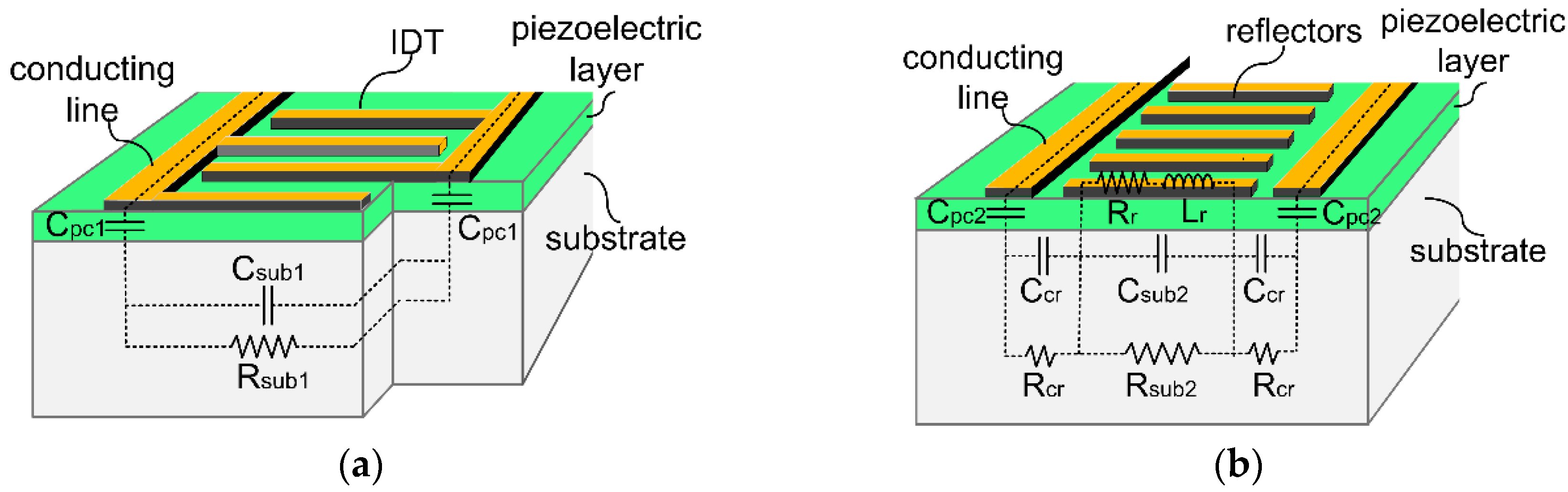
2.2. Parallel Parasitic Parameters Introduced from the Conducting Lines

The semiconducting substrate will also introduce parasitic parameters from the conducting lines which connect the IDT and the port of the stimulating signal. The equivalent circuit components of these parasitic parameters are shown in Figure 3.
As can be seen from Figure 3, both the IDT part (Figure 3a) and reflector part (Figure 3b) will introduce parasitic effects from the substrate.
In the IDT part, each components are outlined as follows: Cpc1 represents the capacitor from the piezoelectric film under the conducting lines, Csub1 represents the capacitor from the substrate between the conducting lines, and Rsub1 represents the resistor from the substrate at the same region.
In the reflector part, Cpc2 represents the same as defined in the IDT part; Rr represents the resistor of the reflecting grids; Rsub2 and Rcr represent the resistors from the substrate lying under and outside the reflector region, respectively; Csub2 and Ccr represent the capacitor from the substrate at the same aforementioned area, respectively; Lr and Rr represents the inductance and resistance from the reflecting grids, respectively.
For these aforementioned parallel parasitic parameters, the analytical formulas can be approximately given as below, among which, Lr is calculated based on the inductance of a flat conductor [23,24]:
C pc 1 = ε 0 ε p l c 1 w c t p
C sub 1 = ε 0 ε s , c l c 1 t s 2 ( w + 2 w i ) + ε 0 ε s , c l c 1 t s 2 w i
R sub 1 = ( ( R ( w + 2 w i ) l c 1 / 2 ) 1 + ( R w i l c 1 / 2 ) 1 ) 1
C pc 2 = ε 0 ε p l c 2 w c t p
R sub 2   = R w l c 2
R cr = R w cr l c 2
C sub 2 = ε 0 ε s , c l c 2 t s w
C cr = ε 0 ε s , c l c 2 t s w cr
R r = ρ m w t m aN r
L r = μ 0 2 Nr π w [ ln ( 2 w a + t m )   + 0.5 + 0.2235 ( a + t m w ) ]
They can be equivalently expressed as an impedance, namely Zep, which is connected in parallel with the SAWR. Zep can be expressed as:
Z ep = R ep + jX ep

2.3. Modified Equivalent Circuit of AlN/Si SAWR

The equivalent circuit model can thus be modified as shown in Figure 4, where the modified equivalent circuit has been shown in Figure 2c. Based on the modified model, the performance of AlN/Si based SAWR can be predicted and compared with the experimental results.

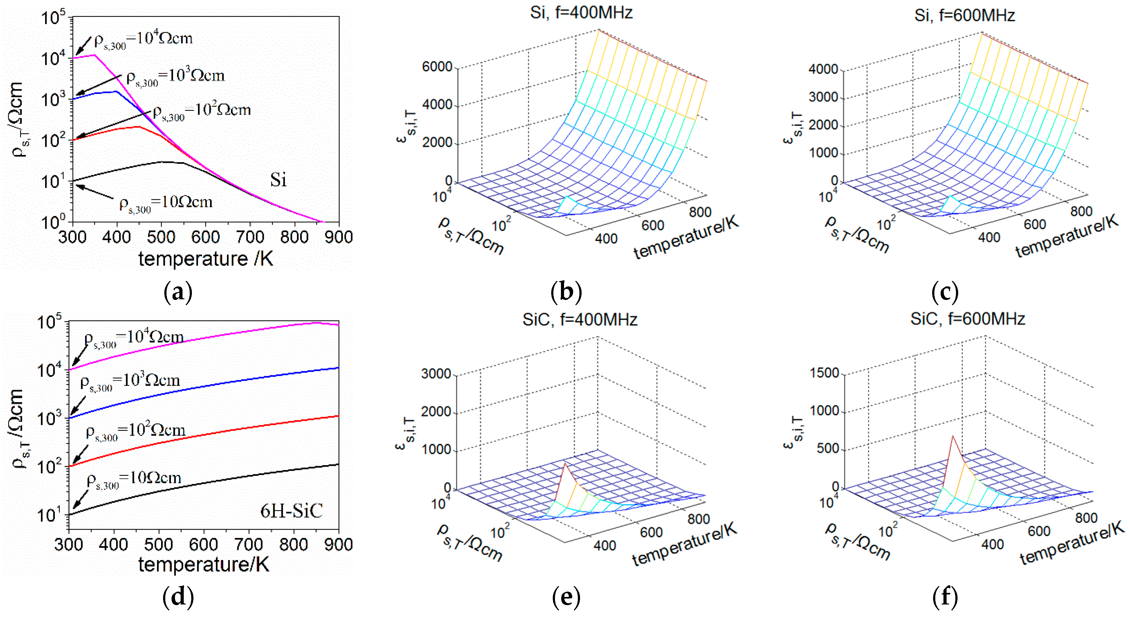
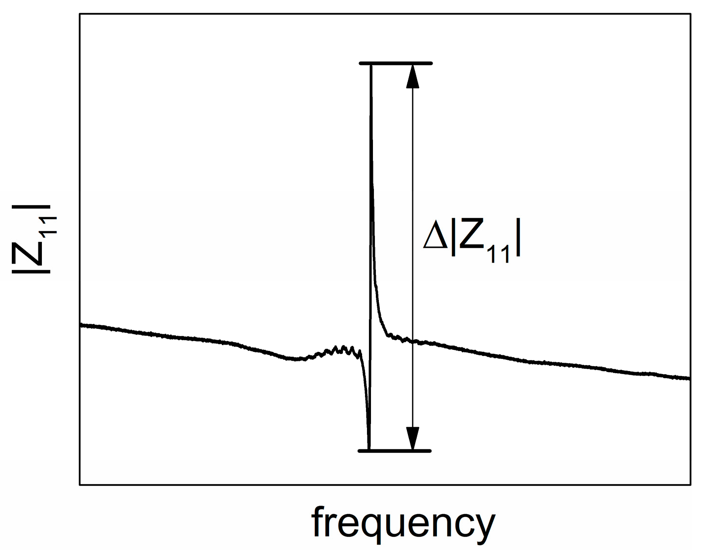
2.4. Temperature Response of Electrical Performance Based on the Modified Equivalent Circuit Model

Temperature will affect the performance of SAWR devices in a complex way due to its coupling with various material properties. These temperature-coupled material properties can be categorized into functioning parameters (such as the electrical-mechanical coupling coefficients), electrical parameters (such the resistivity, relative permittivity) and mechanical parameters (such as elastic constants, mass density). Here in this section, the temperature influence on the SAWR from the aspect of substrate will be analyzed based on the modified equivalent circuit model introduced above.
As can be seen from Section 2.1 and Section 2.2, the parasitic parameters introduced by the semiconducting substrate are related to the square resistance R, the complex relative permittivity εs,c, and the geometric parameters, among which, R can further be calculated through the resistivity ( ρ s ) and the thickness of the substrate ( t s ) as:
R = ρ s t s
Therefore the parasitic parameters influenced by the temperature can further be expressed as functions of ρ s , T , εs,c,T, and aT, being the temperature-dependent resistivity of substrate, temperature-dependent complex relative permittivity of substrate, thermal expansion coefficient, respectively. aT is introduced here due to the variation of geometric parameters from thermal expansion.
For n-type semiconductors discussed here, ρ s , T can further be expressed as [25]:
ρ s , T = ( e μ n , T n T ) 1
where μ n , T and n T are, respectively, the carrier mobility and electron concentration, both being temperature dependent, while e is the elementary charge and not sensitive to temperature. For a dopant concentration N d lower than 10 14 , μ n , T can further be expressed as [25]:
μ n , T   = μ 300 ( T 300 ) 2.2
where μ 300 is the carrier mobility of the substrate under 300 K, and T is the absolute temperature in K. The temperature dependent electron concentration n T can be expressed as [25]:
n T = N d 2 + N d 2 4 + n i , T 2
where n i , T is the intrinsic concentration of electrons, and can further be expressed as [25]:
n i ( T ) = N c , T N v , T e E g 2 kT
where E g is the band gap of the substrate, and k is the Boltzmann constant. N c , T and N v , T are, respectively, the effective density of states for the conduction band and valence band, and can be expressed as [25]:
N C , T = N C 0 T 3 / 2
N V , T = N V 0 T 3 / 2
where N C 0 and N V 0 are the effective density of states coefficients for the conduction band and valence band. The temperature dependent resistivity ρ s , T can thus be given as Equation (25) by combining Equations (19)–(24).
ρ s , T = ( e μ 300 ( T 300 ) 2.2 ( N d 2 + N d 2 4 + N C 0 N V 0 T 3 e E g kT ) ) 1
The complex relative permittivity εs,c,T can be expressed by its real part ε s , r and imaginary part ε s , i , T as [26]:
ε s , c , T = ε s , r j ε s , i , T
while the real part of ε s , c , T is the dielectric constant (εs,R) of the substrate, the imaginary part, being temperature dependent, can be expressed as Equation (27) without considering the electronic and ionic polarization [26], where ε 0 is the dielectric constant of vacuum.
ε s , i , T = 1 2 π ε 0 f ρ s , T
As can be seen from Equation (27), ε s , i , T is a function of ρ s , T and frequency f, where ρ s , T has been given by Equation (25).
Based on the expressions listed above, the temperature response of substrate’s properties can be calculated. The chosen materials of the substrates are Si and 6H-SiC, with the nominal resistivity at 300 K ( ρ s , 300 ) varying from 10 Ωcm to 104 Ωcm. The material parameters used in calculation are listed in Table 1.
The intrinsic concentrations of electrons at 300 K ( n i , 300 ) are firstly calculated by Equation (22), and the dopant concentrations ( N d ) can further be calculated by combing Equations (19)–(21) as:
1 ρ s , 300 = e μ 300 ( N d 2 + N d 2 4 + n i , 300 2 )
The calculated N d with different ρ s , 300 are listed in Table 2.
Through Equations (25) and (27), the calculated ρ s , T and ε s , i , T with different ρ s , 300 and temperatures (300–900 K) are shown in Figure 5.
As shown in Figure 5a, ρ s , T of Si increases slightly and then decreases as the temperature rises, indicating a collaborative effect from the decreasing carrier mobility and increasing electron concentration. At temperatures higher than 600 K, the Si substrate is highly intrinsic, and ρ s , T with different ρ s , 300 become converged. Besides, both of the calculated ε s , i , T of Si at 400 MHz and 600 MHz are showing an increase on orders of magnitude at temperature higher than 600 K, mainly due to the decreasing ρ s , T . As can be seen from Figure 5d, ρ s , T of 6H-SiC with different ρ s , 300 increases through the temperature range of calculation, and shows no convergence of the curves. As for ε s , i , T of 6H-SiC, it doesn’t manifest the increase at elevated temperatures observed in the case of Si. The different behaviors between Si and 6H-SiC are contributed to their different band gaps. 6H-SiC, with a wide band gap, shows less diversification of its electrical properties within the calculated temperature range.
Referring to Equations (1), (2), (8), (9) and (11)–(14), it can be seen that the geometric parameters are on the same order with ρ s , T or εs,c,T, and considering that Si’s and 6H-SiC’s coefficients of thermal expansion range from around 2 ppm/C to 5 ppm/C in the temperature range of 300 to 900 K [28,29], which is much lower than the relative changes of ρ s , T or εs,c,T, the effect from thermal expansion can be neglected.
With the calculated ρ s , T and ε s , i , T , the temperature performance of SAWR can thus be derived through the modified equivalent circuit model introduced in this work. The geometric parameters and material properties used in the calculation are listed in Table A1 of Appendix A. And molybdenum (Mo) is chosen as the metal material for IDT and reflectors for its high melting point and close lattice constants with AlN. To evaluate the performance fluctuation of SAWR, the magnitude of the impedance ( | Z 11 | ) is utilized. A typical frequency domain | Z 11 | curve of SAWR in frequency domain is shown in Figure 6, from which the serial and parallel resonant frequencies can be derived. In this work, Δ | Z 11 | , which is the difference between the | Z 11 | at both the serial and parallel resonant frequencies, is used to indicate the strength of the electrical tuning of the SAWR.
SAWRs with configurations of AlN/Si and AlN/6H-SiC are modeled within a temperature range from 300 K to 900 K, the temperature dependence of Δ | Z 11 | for each configuration is calculated and normalized by using the result when ρ s , 300 = 10 4 Ωcm and T = 300 K as a reference. As can be seen from Figure 7a,b, a decrease of Δ | Z 11 | is shown in AlN/Si SAWR for every initial ρ s , 300 , while in the case of AlN/6H-SiC, opposite responses are observed, indicating a more stable device performance could be achieved by using 6H-SiC as the substrate. The contrary performances between the two configurations can be contributed to the different electrical characteristics with temperature of Si and 6H-SiC, which has been discussed above.

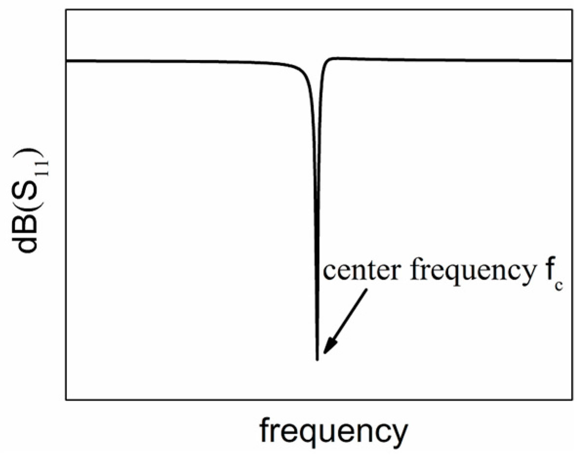
2.5. Temperature Response of Center Frequency

Except for the electrical performance of SAWR discussed in previous section, the TCF is another important parameter when evaluating the temperature response to SAWR devices. In this work, the TCF of SAWR’s center frequency ( f c ) is analyzed theoretically and experimentally. The center frequency can be derived through the frequency domain reflection coefficient (S11), corresponding to the frequency with the lowest S11 as shown in Figure 8.
For the theoretical analysis of f c , it can be calculated by the SAW velocity ( v SAW ) and wavelength ( λ SAW ) as:
f c = v SAW / λ SAW
Considering λ SAW equals the geometric period of IDT (λ), which along with v SAW , are all functions of temperature, therefore Equation (29) can further be expressed as:
f c , T = v SAW , T / λ T
By taking the center frequency at 300 K ( f c , 300 ) as a reference, the TCF of SAR ( TCF SAW ) can be expressed as:
TCF SAW = f c , T f c , 300 f c , 300 Δ T = 1 Δ T v SAW , T v SAW , 300 v SAW , 300 1 Δ T λ T λ 300 λ 300
where v SAW , 300 and λ 300 are the SAW velocity and geometric period of IDT at 300 K, respectively.
The first term of Equation (31) represents the TCF of SAW velocity. For the hexagonal crystallized and cubic crystallized materials (Si, 6H-SiC, AlN) discussed in this work, the SAW velocity can be expressed by the mass density ( ρ ) and the elastic constants ( c ij ) as [30,31]:
c 33 c 55 ( ρ v SAW ) 2 ( c 11   ρ v SAW ) = ( c 55 ρ v SAW ) [ c 33 ( c 11   ρ v SAW ) c 13 2 ] 2
By taking temperature into consideration, v SAW , T can thus be expressed as:
v SAW,T = f ( ρ T , c ij,T )
where ρ T is the mass density under temperature T and can be given by:
ρ T = ρ 300 ( 1 Δ T m a T , m ¯ )
ρ 300 is the mass density at 300 K, a T , m ¯ is the effective thermal expansion coefficient of the material along m-axis (m = x, y, z), representing the average expansion rate through 300 K to (300 +   Δ T )K, and can be calculated as:
a T , m ¯ = 1 Δ T 300 300 + Δ T a T , m ( T ) dT
c ij,T in Equation (33) represents the elastic constants under temperature T, and can be calculated by:
c ij,T = c ij , 300 ( 1 + Δ T dc ij c ij dT )
For the second term of Equation (31), noticing that in the coordinate system defined in Figure 1, SAW propagates along the x-axis, hence λ T can be expressed as:
λ T = λ 300 ( 1 + a T , x ¯ Δ T )
By taking Equations (37) into (31), Equation (31) can further be expressed as:
TCF SAW = 1 Δ T v SAW , T v SAW , 300 v SAW , 300 a T , x ¯
The TCF SAW of AlN, Si, 6H-SiC can thus be calculated and shown in Table 3, in addition to the parameters listed in Table A1 of Appendix A, all other parameters used in calculation have been listed in Table A2 of Appendix A [28,29,32,33,34,35,36].
It is known that the energy of SAW is constrained within several wavelengths beneath the surface of IDT plane [18], hence with a wavelength larger than the thickness of AlN in this work, the actual TCF SAW of AlN/Si and AlN/6H-SiC based SAWR will be decided by both the piezoelectric film (AlN) and the substrate (Si or 6H-SiC). Besides, the mismatch of thermal expansions between AlN and the substrate in the x-y plane will also introduce thermal mismatch strains, namely Δ ε T , which can be calculated by the thermal expansion of material in free and layered conditions, as:
Δ ε T = ε T , free ε T , layered
where ε T , free is the ideal thermal expansion of free material, and ε T , layered is the thermal expansion of material in the layered structure. Consideringthe much larger thickness of the substrate than that of AlN, the thermal expansions of the AlN/Si and AlN/6H-SiC based SAWRs are decided by the substrates, hence the thermal mismatch strains of the substrates can be neglected, and the strain of AlN is not sensitive to the film thickness, both of which has been confirmed by finite element modeling results. For each of the AlN layers in the calculated AlN/Si and AlN/6H-SiC based SAWRs, with the premise that it is isotropic in the x-y plane, the Δ ε T of each configuration is calculated and shown in Figure 9.
With the given strain field ε = [ Δ ε T , Δ ε T , 0 ] , the relative change of f c can thus be calculated by:
Δ f c f c = f c , ε f c , 0 ε f c , 0 ε = v SAW , ε   v SAW , 0 ε v SAW , 0 ε     λ ε   λ 0 ε λ 0 ε
Therefore the TCF introduced by the thermal strain mismatch can be expressed as:
TCF ε = f c , ε f c , 0 ε Δ Tf c , 0 ε = v SAW , ε   v SAW , 0 ε Δ Tv SAW , 0 ε     λ ε   λ 0 ε Δ T λ 0 ε
where λ ε and λ 0 ε are the geometric period of IDT with strain ε and without ε , and has the relationship:
λ ε = λ 0 ε ( 1 + Δ ε T )
Similarly, v SAW , ε and v SAW , 0 ε are, respectively, the SAW velocity under the appearance and absence of strain ε . As shown in Equation (32), v SAW can be given by the elastic constant and the mass density, which are both functions of strain field ε , therefore v SAW , ε can be given as:
v SAW , ε = f ( ρ ε , c ij , ε )
where ρ ε is the mass density under strain field and can be given by:
ρ ε = ρ 0 ε ( 1 2 Δ ε T )
where c ij , ε represents the elastic constants of AlN in strain field, and can be calculated by the third order elastic constants c ijk as given by references [36,37,38] and written as Equation (45) for simplicity. The third order elastic constants used for calculation has been in Table A2 of Appendix A.
c ij ( ε ) = f ( c ij , c ijk , ε )
The calculated TCF ε of AlN in AlN/Si and AlN/6H-SiC configurations are −0.03 ppm/K and −0.02 ppm/K.
As can be seen, the TCF ε of AlN in both of the calculated configurations are orders of magnitude lower than the intrinsic TCFSAW of AlN listed in Table 3, therefore the TCF ε has little influence on the total TCF of the AlN layer in either SAWR configuration.

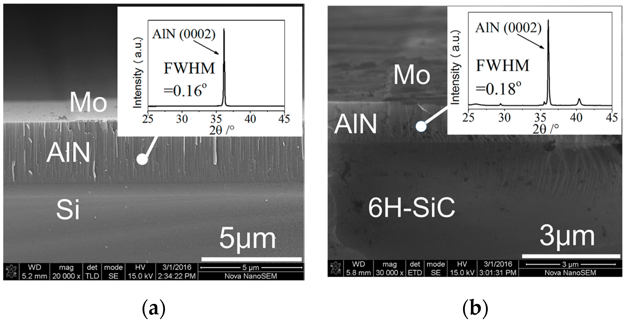
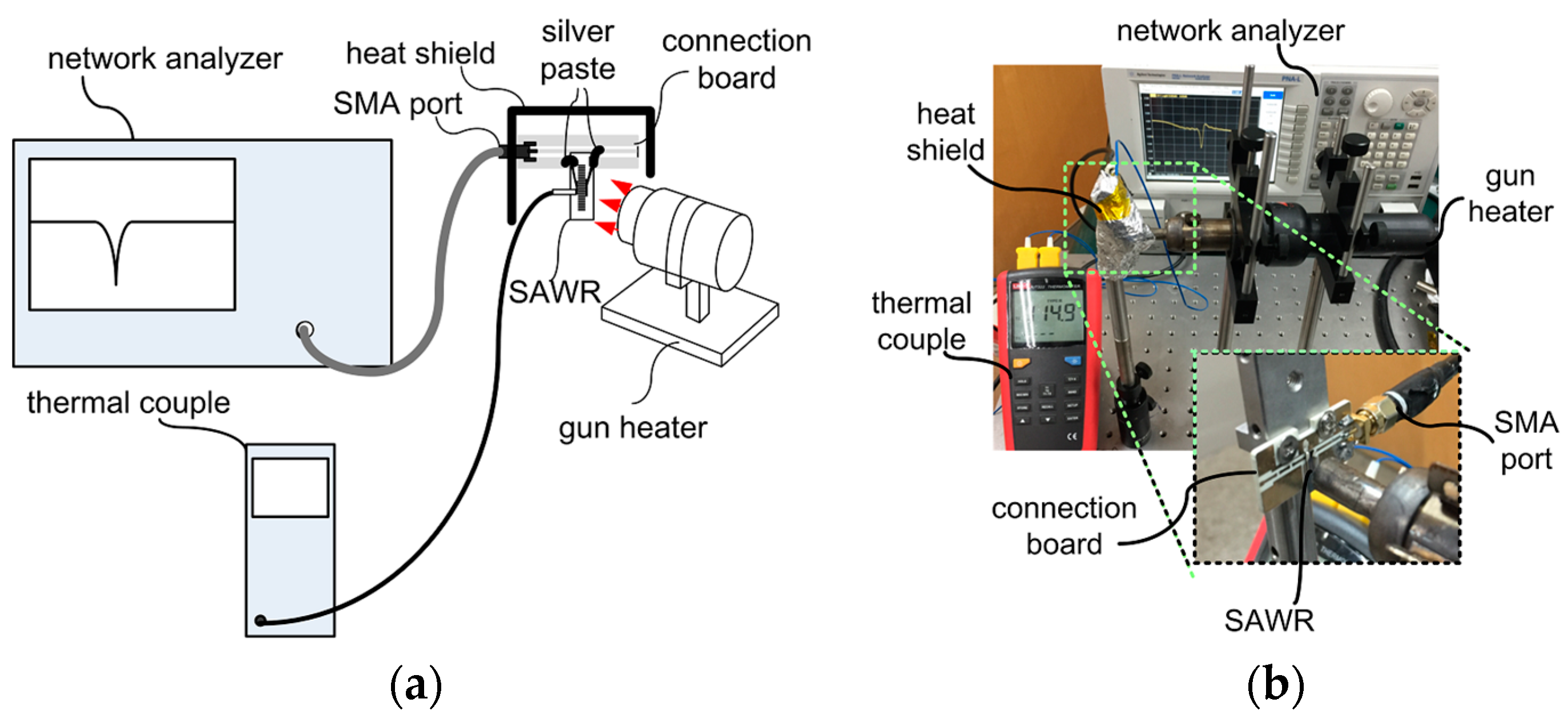
3. Experimental Section

The fabricated AlN/Si and AlN/6H-SiC SAWRs in this work has the same layout design, as has been given by Table A1 of Appendix A.
For the AlN/Si configuration, a 400 μm thick, 4″ n-type (100) silicon wafer is prepared as substrate, and cleaned with buffer hydrofluoric acid (BHF), acetone, isopropanol (IPA) and deionized water. The resistivity of the substrate is around 4.5 × 10³ Ωcm (4-Probe method, NPS RESISTEST VIII). Polycrystalline AlN layer with a thickness of 3 μm is deposited on the Si substrate via RF sputtering, followed by 100 nm thick of Mo deposited with the same method. The Mo layer is patterned into the designed layout by reactive ion etching (RIE). A gold (Au) layer of 100 nm in thickness is then evaporated and patterned as electrodes for signal connection.
As for the AlN/6H-SiC configuration, a 350 μm thick, 4″ n-type (0002) 6H-SiC wafer is chosen as the substrate, with a nominal resistivity higher than 1 × 10⁵ Ωcm. The same micro fabrication process is utilized for fabricating the SAWR as in the case of AlN/Si configuration. It should be noted that besides the thickness of the substrate, the thickness of AlN film in AlN/6H-SiC configuration, being 1.5 μm, is also different from that of AlN/Si configuration due to the fabrication capability. But since this work mainly focuses on the relative fluctuation of each configuration under different temperatures, these inconsistencies will have little effect on the results and conclusions.
An abbreviated fabrication process has been illustrated in previously reported work [38]. The AlN films in both configurations are characterized by X-ray diffraction (XRD) spectrum, and the Mo/AlN/substrate layered stacks are characterized by scanning electrons microscope (SEM).
After the micro-fabrication process, SAWRs are diced from wafers and adhered to connection board by high temperature adhesion agent. High temperature silver paste (SX-9302) is used to electrically connect the SAWR devices and connections boards.
The high temperature range responses of the SAWRs are then tested from 300 to 725 K with the apparatus shown in Figure 10. The SAWRs are heated by a gun heater (ATTEN instrument), with the temperature monitored by thermocouples (Uni-Trend Technology, UT322). The frequency domain response of the SAWRs is monitored and recorded by network analyzer (Agilent Technology, N5230C) simultaneously. Temperature responses of both electrical performance and center frequency are evaluated and compared with the modeling and calculated results.

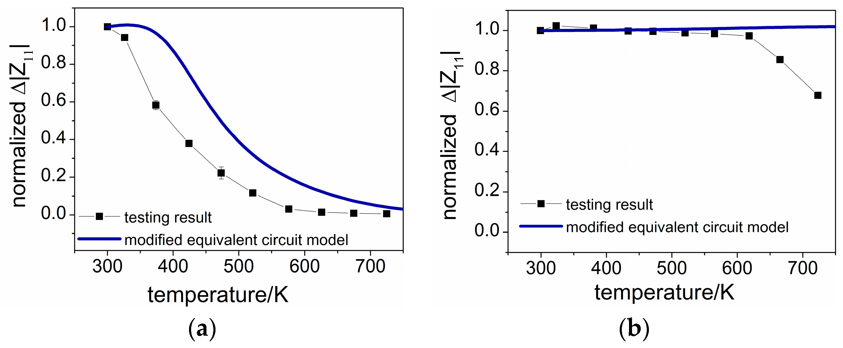
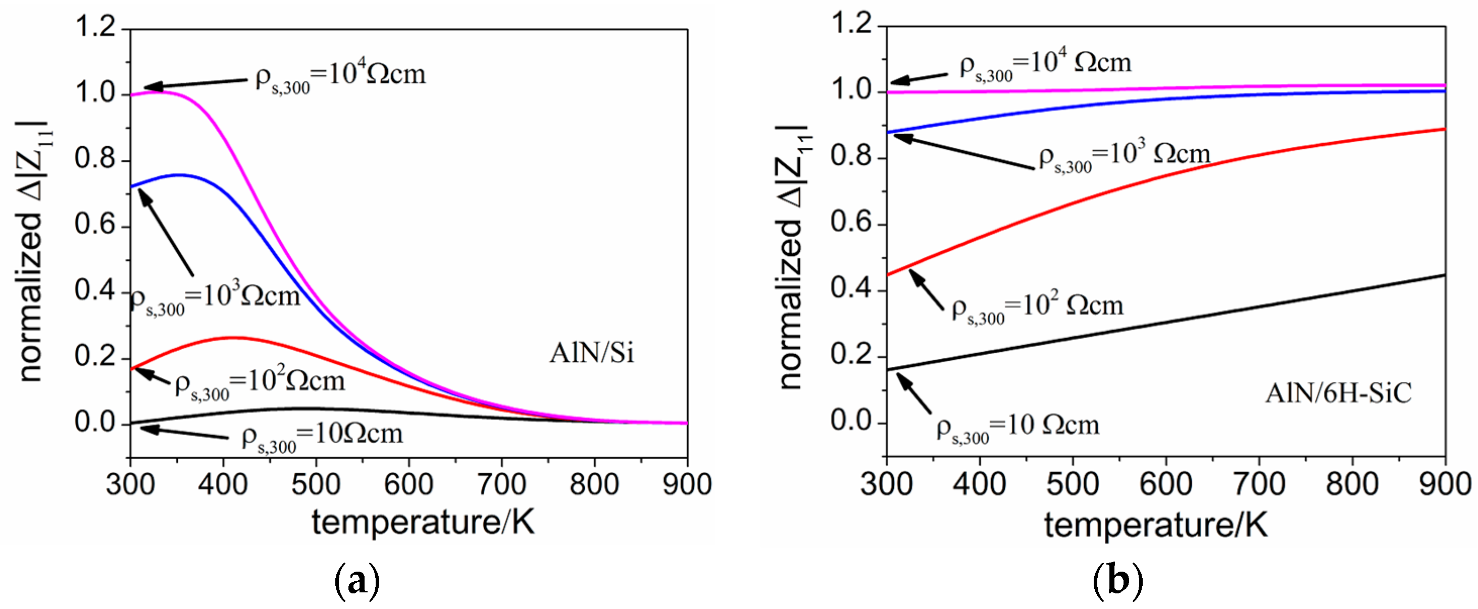
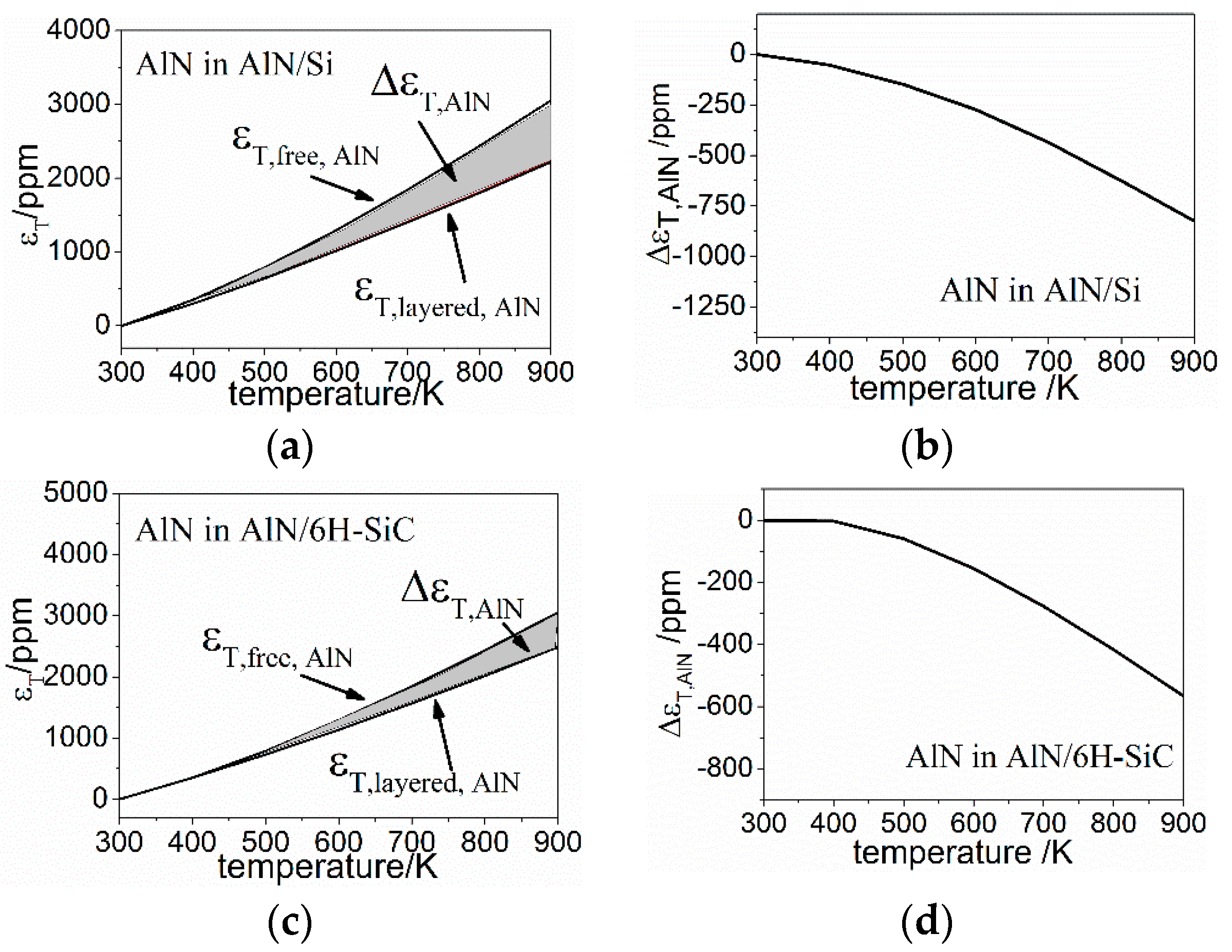
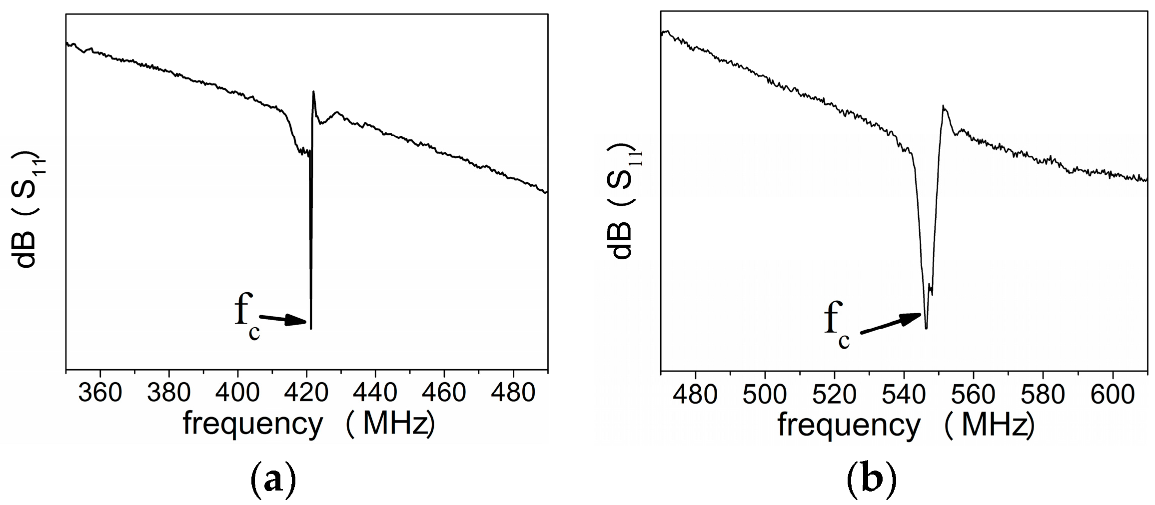
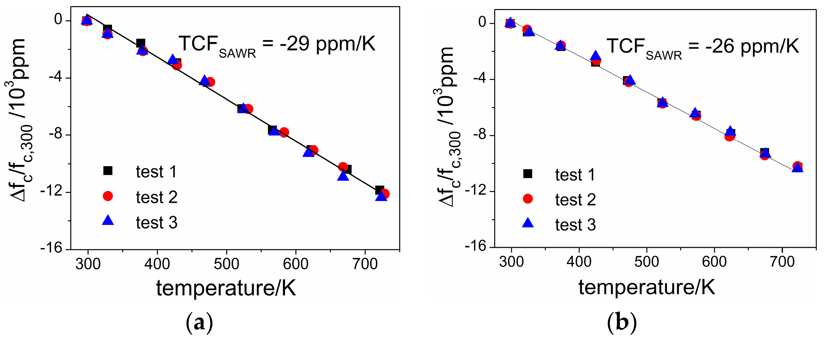
4. Results and Discussion

The XRD and SEM characterizations of the as-deposited AlN on both Si and 6H-SiC are shown in Figure 11. The full width at half maximum (FWHM) of the (0002)-AlN can be derived from the XRD spectrum and are 0.16° and 0.18° for the AlN/Si and AlN/6H-SiC configuration, respectively, indicating highly c-axis oriented (0002) AlN has been grown on each substrate.
The center frequency of the fabricated AlN/Si SAWR is 422 MHz, while that of AlN/6H-SiC is 546 MHz. The typical reflection coefficient S11 of both configurations have been shown in Figure 12.
The electrical performances of SAWRs under different temperatures are evaluated by analyzing the frequency domain response of each configuration. Similar to the method mentioned in the modeling part, Δ | Z 11 | of each temperature point is used for the comparison, and the values of Δ | Z 11 | are normalized by using the room temperature (300 K) data for comparison. The tested results are shown in Figure 13a,b.
As can be seen, the Δ | Z 11 | of AlN/Si configuration decreases fast with an increasing temperature, while that for AlN/6H-SiC configuration degrades less than 5% within 625 K, which are in accordance with the predicted performances given by the modified equivalent circuit model.
The differences between the modeling and experimental results may come from the serial parasitic parameters such as the resistors and inductors introduced by the IDT grids and the conducting lines, which are not considered in the modeling here but also vary with temperature. Another possible contributing factor to the differences is the lattice vibration [39], leading to stronger acoustic scattering and phonon loss at elevated temperatures, which may lead to a deterioration stronger than the modeling results and play a dominating role at higher temperatures, as shown in the AlN/6H-SiC configuration at temperatures higher than 650 K.
After all, based on the modeling and experimental results shown in this work, it can be inferred that the semiconductor property of the substrate, mostly the band gap, is playing a key role in the electrical performance of the AlN-film based SAWR, and substrates with a higher band-gap will lead to a more stable high temperature performance.
The temperature responses of center frequency are also tested for both configurations and linear approximation is used for deriving the first order TCFSAWR, as shown in Figure 14. The first order TCFSAWR of −29 ppm/K is obtained for the AlN/Si configuration, and −26 ppm/K for the AlN/SiC one. As has been shown in Section 2.5, the frequency shift due to thermal mismatch is negligible compared to the intrinsic TCFSAW of the materials discussed in this work, therefore the differences between the calculated TCFSAWR (−26~−28 ppm/K for the AlN/Si configuration and −25~−28 ppm/K for the AlN/6H-SiC configuration) can be contributed to the inconformity of the actual parameter and those used in calculation, especially the temperature coefficient factors of elastic constants ( 1 Δ T Δ c ij c ij ), which are sensitive to testing methods and have existing inconsistencies among different research reports.
Considering the relative mismatch of the calculated TCFSAWR to the experimental one is less than 15% in each configuration, the method induced in this work is an effective way for estimating the TCF of AlN-film based SAWRs, which would be important when designing SAWR-based sensors working in a wide temperature range and if temperature compensation being needed.

5. Conclusions

The temperature responses of aluminum nitride (AlN) film based surface acoustic wave resonators (SAWR) are modeled and tested. A modified equivalent circuit model is introduced to model the electrical performance in a varying temperature environment. By taking the parasitic parameters from the substrate into the modeling, the electrical performances of the AlN-film based SAWRs can be predicted, and are further compared with high temperature experiments from 300 K to 725 K, leading to a conclusion that SAWR based on substrates with wider band gaps will lead to a more stable high temperature behavior.
Temperature responses of SAWR’s center frequency are also calculated and tested, with experimental TCFSAWR of center frequencies being −29 ppm/K and −26 ppm/K for the AlN/Si and AlN/6H-SiC based SAWRs. Considering the relative mismatch is less than 15% between calculated TCFSAWR and the experimental ones, the calculation method introduced in this work is an effective way for estimating the TCF of AlN-film based SAWRs, which would be important when designing SAWR-based sensors working in a wide temperature range as well as temperature compensation.

Acknowledgments

The authors gratefully acknowledge the Institute of Gas Turbine (Tsinghua University) and the Tsinghua-Berkeley funds for the financial support of this work.

Author Contributions

For the work reported in this article, Shuo Chen and Zheng You motivated and conducted the model design and modification. Shuo Chen designed and performed the experiment, analyzed the data, and wrote the paper.

Conflicts of Interest

The authors declare no conflict of interest.

Abbreviations

The following abbreviations are used in this manuscript:
SAWRSurface acoustic wave resonator
TCFTemperature coefficient factor
IDTInter-digital transducer
FWHMFull width at half maximum

Appendix A

The geometric and material parameters used for modeling and calculation in this work are listed in Table A1.
Table A1. Material parameters used for modeling and calculation (Cij represents the elastic constants of material, i,j = 1~6).
ParametersValue/UnitParametersValue/Unit
c11,AlN408.03/GPac44,SiC137/GPa
c12,AlN100.18/GPac66,SiC153/GPa
c13,AlN83.40/GPa ρ 300 , SiC 3216/kg·m−3
c33,AlN384.30/GPa ε SiC , R 9.7
c44,AlN100.08/GPats,Si400/μm
c66,AlN153.93/GPatp,AlN-Si3/μm
ρ 300 , AlN 3260/kg·m−3ts,SiC400/μm
ε AlN , R 9tp,AlN-SiC3/μm
c11,Si165.63/GPatm100/nm
c12,Si63.87/GPaN50
c44,Si79.55/GPaλ12/μm
ρ 300 , Si 2329/kg·m−3a3/μm
c11,Mo440.77/GPaw840/μm
c12,Mo172.43/GPaNR600
c44,Mo121.65/GPalc1600/μm
ρ Mo 10,200/kg·m−3lc25000/μm
ε Si , R 11.7wc200/μm
c11,SiC493/GPalt7.5/μm
c12,SiC187/GPawcr480/μm
c13,SiC91/GPawi40/μm
c33,SiC553/GPaK20.2%
Table A2. Material parameters used for modeling and calculation (complementary parameters) [28,29,32,33,34,35,37].
ParametersValue/UnitParametersValue/Unit
a T , x , AlN ref. [32] 1 Δ T Δ c 13 , Si c 13 , Si ref. [34]
a T , y , AlN ref. [32] 1 Δ T Δ c 11 , SiC c 11 , SiC ref. [35]
a T , z , AlN ref. [32] 1 Δ T Δ c 33 , SiC c 33 , SiC ref. [35]
a T , x , Si ref. [28] 1 Δ T Δ c 44 , SiC c 44 , SiC ref. [35]
a T , y , Si ref. [28] 1 Δ T Δ c 13 , SiC c 13 , SiC ref. [35]
a T , z , Si ref. [28]c111,AlN−3072.30/GPa
a T , x , SiC ref. [29]c112,AlN−514.07/GPa
a T , y , SiC ref. [29]c113,AlN−75.06/GPa
a T , z , SiC ref. [29]c123,AlN−155.12/GPa
1 Δ T Δ c 11 , AlN c 11 , AlN −37/ppmK−1c133,AlN−614.88/GPa
1 Δ T Δ c 33 , AlN c 33 , AlN −65/ppmK−1c344,AlN−576.45/GPa
1 Δ T Δ c 44 , AlN c 44 , AlN −50/ppmK−1c144,AlN−150.12/GPa
1 Δ T Δ c 55 , AlN c 55 , AlN −50/ppmK−1c155,AlN−100.08/GPa
1 Δ T Δ c 13 , AlN c 13 , AlN −1.8/ppmK−1c222,AlN−2413.0/GPa
1 Δ T Δ c 11 , Si c 11 , Si ref. [34]c333,AlN−2213.6/GPa
1 Δ T Δ c 44 , Si c 44 , Si ref. [34]

References

  1. Thiele, J.A.; da Cunha, M.P. High temperature LGS SAW gas sensor. Sens. Actuator B 2006, 113, 816–822. [Google Scholar] [CrossRef]
  2. Benetti, M.; Cannata, D.; di Pietrantonio, F.; Marchiori, C.; Persichetti, P.; Verona, E. Pressure sensor based on surface acoustic wave resonators. In Proceedings of the 2008 IEEE on Sensors, Lecce, Italy, 26–29 October 2008; pp. 1024–1027.
  3. García-Gancedo, L.; Milne, W.I.; Luo, J.K.; Flewitt, A.J. Sensors based on SAW and FBAR technologies. In Proceedings of the 4th International Conference on Smart Materials and Nanotechnology in Engineering, International Society for Optics and Photonics, Gold Coast, Australia, 10 July 2013; pp. 879308–879308-7.
  4. Pohl, A. A review of wireless SAW sensors. IEEE Trans. Ultrason. Ferroelectr. Freq. Control 2000, 47, 317–332. [Google Scholar] [CrossRef] [PubMed]
  5. Zhang, S.; Yu, F. Piezoelectric materials for high temperature sensor. J. Am. Ceram. Soc. 2011, 10, 3153–3170. [Google Scholar] [CrossRef]
  6. Hornsteiner, J.; Born, E.; Fischerauer, G.; Riha, E. Surface acoustic wave sensors for high-temperature applications. In Proceedings of the 1998 IEEE International Frequency Control Symposium, Pasadena, CA, USA, 27–29 May 1998; pp. 615–620.
  7. Farrell, R.; Pagán, V.R.; Kabulski, A.; Kuchibhatla, S.; Harman, J.; Kasarla, K.R. High temperature annealing studies on the piezoelectric properties of thin aluminum nitride films. In MRS Online Proceeding Library; Cambridge University Press: Cambridge, UK, 2008. [Google Scholar]
  8. Lai, Y.J.; Li, W.C.; Lin, C.M.; Felmetsger, V.V.; Pisano, A.P. High-temperature stable piezoelectric aluminum nitride energy harvesters utilizing elastically supported diaphragms. In Proceedings of the IEEE Transducers & Eurosensors, Barcelona, Spain, 16–20 June 2013; pp. 2268–2271.
  9. Piazza, G.; Felmetsger, V.; Muralt, P.; Olsson III, R.H.; Ruby, R. Piezoelectric aluminum nitride thin films for microelectromechanical systems. MRS Bull. 2012, 37, 1051–1061. [Google Scholar] [CrossRef]
  10. Lin, C.M.; Yantchev, V.; Zou, J.; Chen, Y.Y.; Pisano, A.P. Micromachined one-port aluminum nitride lamb wave resonators utilizing the lowest-order symmetric mode. J. Microelectromech. Syst. 2014, 23, 78–91. [Google Scholar] [CrossRef]
  11. Lin, C.M.; Chen, Y.Y.; Felmetsger, V.V.; Senesky, D.G.; Pisano, A.P. AlN/3C-SiC composite plate enabling high-frequency and high-Q micromechanical resonators. Adv. Mater. 2012, 24, 2722–2727. [Google Scholar] [CrossRef] [PubMed]
  12. Benetti, M.; Cannata, D.; di Pictrantonio, F.; Verona, E. Growth of AlN piezoelectric film on diamond for high-frequency surface acoustic wave devices. IEEE Trans. Ultrason. Ferroelectr. Freq. Control 2005, 52, 1806–1811. [Google Scholar] [CrossRef] [PubMed]
  13. Lin, C.M.; Lien, W.C.; Felmetsger, V.V.; Hopcroft, M.A.; Senesky, D.G.; Pisano, A.P. AlN thin films grown on epitaxial 3C-SiC (100) for piezoelectric resonant devices. Appl. Phys. Lett. 2010, 97, 141907. [Google Scholar] [CrossRef]
  14. Blampain, E.; Elmazria, O.; Aubert, T.; Assouar, B.; Legrani, O. Surface acoustic wave sensor based on AlN/Sapphire structure for high temperature and high frequency applications. In Proceedings of the 2011 IEEE on Sensors, Limerick, Ireland, 28–31 October 2011; pp. 610–613.
  15. Liaw, H.M.; Cronin, W.; Hickernell, F.S. The SAW characteristics of sputtered aluminum nitride on silicon. In Proceedings of the IEEE Ultrasonics Symposium, Cannes, France, 31 October–3 November 1994; pp. 267–271.
  16. Lin, C.M.; Chen, Y.Y.; Felmetsger, V.V.; Yen, T.T.; Lien, W.C.; Senesky, D.G.; Pisano, A.P. Surface acoustic wave propagation properties in AlN/3C-SiC/Si composite structure. In Proceedings of the IEEE Ultrasonics Symposium, San Diego, CA, USA, 11–14 October 2010; pp. 1696–1699.
  17. Zhu, L.; Li, Q.; Liu, K. Modeling of one-port SAW resonator based on ADS. Piezoelectr. Acoustoopt. 2012, 34, 17–23. [Google Scholar]
  18. Hashimoto, K.Y. Surface Acoustic Wave Devices in Telecommunications; Springer: Berlin, Germany, 2000. [Google Scholar]
  19. Kojima, T.; Shibayama, K. An analysis of reflection characteristics of the surface-acoustic-wave reflector by an equivalent circuit model. Jpn. J. Appl. Phys. 1987, 26, 117–119. [Google Scholar] [CrossRef]
  20. Smith, W.R.; Gerard, H.M.; Collins, J.H.; Reeder, H.M.; Shaw, H.J. Analysis of interdigital surface wave transducers by use of an equivalent circuit model. IEEE Trans. Microw. Theory Tech. 1969, 17, 856–864. [Google Scholar] [CrossRef]
  21. Tang, G.; Han, T.; Teshigahara, A.; Iwaki, T. Enhancement of effective electromechanical coupling factor by mass loading in layered SAW device structures. In Proceedings of the 2015 Joint Conference of the IEEE International Frequency Control Symposium & the European Frequency and Time Forum, Denver, CO, USA, 12–16 April 2015; pp. 416–419.
  22. Blampain, E.; Elmazria, O.; Legrani, O.; McMurtry, S.; Montaigne, F.; Fu, C.; Yang, S.S. Platinum/AlN/Sapphire SAW resonator operating in GHz range for high temperature Wireless SAW sensor. In Proceedings of the IEEE Ultrasonics Symposium (IUS), Prague, Czech, 21–25 July 2013; pp. 1081–1084.
  23. Kazimierczuk, M.K. High-Frequency Magnetic Components; John Wiley & Sons: New York, NY, USA, 2009. [Google Scholar]
  24. Wadell, B.C. Transmission Line Design Handbook; Artech House Publishers: Boston, MA, USA, 1991. [Google Scholar]
  25. Neamen, D. An Introduction to Semiconductor Devices; McGraw-Hill, Inc.: New York, NY, USA, 2005. [Google Scholar]
  26. Krupka, J.; Breeze, J.; Centeno, A.; Alford, N. Measurements of permittivity, dielectric loss tangent, and resistivity of float-zone silicon at microwave frequencies. IEEE Trans. Microw. Theory Tech. 2006, 54, 3995–4001. [Google Scholar] [CrossRef] [Green Version]
  27. Shur, M.; Rumyantsev, S.; Levinshtein, M. SiC Materials and Devices; World Scientific: Singapore, 2006. [Google Scholar]
  28. Okaji, M. Absolute thermal expansion measurements of single-crystal silicon in the range 300–1300 K with an interferometric dilatometer. Int. J. Thermophys. 1988, 9, 1101–1109. [Google Scholar] [CrossRef]
  29. Li, Z.; Bradt, R.C. Thermal expansion and thermal expansion anisotropy of sic polytypes. J. Am. Ceram. Soc. 1987, 70, 445–448. [Google Scholar] [CrossRef]
  30. Royer, D.; Dieulesaint, E. Rayleigh wave velocity and displacement in orthorhombic, tetragonal, hexagonal, and cubic crystals. J. Acoust. Soc. Am. 1985, 76, 1438–1444. [Google Scholar] [CrossRef]
  31. Littles, J.W., Jr.; Jacobs, L.J.; Zureick, A.H. The ultrasonic measurement of elastic constants of structural FRP composites. In Quantitative Nondestructive Evaluation; Springer US: New York, NY, USA, 1997; pp. 1807–1814. [Google Scholar]
  32. Wang, K.; Reeber, R.R. Thermal expansion of GaN and AlN. MRS Online Proc. Libr. 2011, 482, 863–868. [Google Scholar] [CrossRef]
  33. Lin, C.M. Temperature-compensated and high-q piezoelectric aluminum nitride lamb wave resonators for timing and frequency control applications. Ph.D. Thesis, The University of California, Berkeley, CA, USA, 2013. [Google Scholar]
  34. Schall, J.D.; Gao, G.; Harrison, J.A. Elastic constants of silicon materials calculated as a function of temperature using a parametrization of the second-generation reactive empirical bond-order potential. Phys. Rev. B 2008. [Google Scholar] [CrossRef]
  35. Li, Z.; Bradt, R.C. The single crystal elastic constants of hexagonal sic to 1000 °C. Int. J. High Technol. Ceram. 1988, 4, 1–10. [Google Scholar] [CrossRef]
  36. Pandey, D.K.; Yadav, R.R. Temperature dependent ultrasonic properties of aluminium nitride. Appl. Acoust. 2009, 70, 412–415. [Google Scholar] [CrossRef]
  37. Rao, R.R.; Padmaja, A. Effective second-order elastic constants of a strained crystal using the finite strain elasticity theory. J. Appl. Phys. 1987, 62, 440–443. [Google Scholar] [CrossRef]
  38. Chen, S.; You, Z. Prediction of the strain response of poly-AlN/(100)Si surface acoustic wave resonator and experimental analysis. Sensors 2016. [Google Scholar] [CrossRef] [PubMed]
  39. Li, C.; Liu, X.; Shu, L.; Li, Y. AlN-based surface acoustic wave resonators for temperature sensing applications. Mater. Exp. 2015, 35, 408–411. [Google Scholar] [CrossRef]
Figure 1. The equivalent circuit model of SAWR.
Sensors 16 01205 g001
Figure 2. Modified equivalent circuit model of the IDT part. (a) Schematic view of the SAWR and the equivalent circuit components; (b) Layout and geometric definitions of SAWR in this work; (c) Modified equivalent circuit of N-pair IDT.
Sensors 16 01205 g002aSensors 16 01205 g002b
Figure 3. Parallel parasitic parameters from the piezoelectric film and the semiconducting substrate (a) IDT part; (b) Reflector part.
Sensors 16 01205 g003
Figure 4. Modified equivalent circuit model.
Sensors 16 01205 g004
Figure 5. Calculated ρ s , T and ε s , i , T with different ρ s , 300 and temperatures (a) ρ s , T of Si; (b) ε s , i , T of Si at 400 MHz; (c) ε s , i , T of Si at 600 MHz; (d) ρ s , T of 6H-SiC; (e) ε s , i , T of 6H-SiC at 400 MHz; (f) ε s , i , T of 6H-SiC at 600 MHz.
Sensors 16 01205 g005
Figure 6. Typical | Z 11 | curve of SAWR in frequency domain.
Sensors 16 01205 g006
Figure 7. Temperature dependences of Δ | Z 11 | for both AlN/Si and AlN/6H-SiC based SAWRs (a) AlN/Si based SAWR; (b) AlN/6H-SiC based SAWR.
Sensors 16 01205 g007
Figure 8. Typical S11 curve of SAWR in frequency domain.
Sensors 16 01205 g008
Figure 9. Temperature dependences of Δ ε T in AlN layer for both AlN/Si and AlN/6H-SiC based SAWRs (a,b) AlN in AlN/Si based SAWR; (c,d) AlN in AlN/6H-SiC based SAWR.
Sensors 16 01205 g009
Figure 10. Apparatus used for temperature response testing (a) Designed diagram; (b) Photo.
Sensors 16 01205 g010
Figure 11. Characterization of the layered SAWR device (a) XRD and SEM characterization of AlN/Si configuration; (b) XRD and SEM characterization of AlN/6H-SiC configuration.
Sensors 16 01205 g011
Figure 12. Typical reflection coefficient of the AlN/Si SAWR in this work (a) AlN/Si based SAWR; (b) AlN/6H-SiC based SAWR.
Sensors 16 01205 g012
Figure 13. Electrical performances of SAWRs under different temperatures (a) AlN/Si based SAWR; (b) AlN/6H-SiC based SAWR.
Sensors 16 01205 g013
Figure 14. Electrical performances of SAWRs under different temperature (a) AlN/Si based SAWR; (b) AlN/6H-SiC based SAWR.
Sensors 16 01205 g014
Table 1. Material parameters used in calculating ρ s , T [25,27].
ParametersValueUnitParametersValueUnit
μ 300 , Si 1350 cm/Vs N C 0 , Si 5.41 × 1015cm−3K−3/2
μ 300 , SiC 400cm/Vs N V 0 , Si 2.19 × 1015cm−3K−3/2
ρ s , Si , 300 10, 102, 103, 104Ωcm N C 0 , SiC 17.3 × 1015cm−3K−3/2
ρ s , SiC , 300 10, 102, 103, 104Ωcm N V 0 , SiC 4.80 × 1015cm−3K−3/2
E g , Si 1.12eVe1.6 × 10−19C
E g , SiC 3.0eV k 1.3806 × 10⁻²³J/K
Table 2. Calculated N d with different ρ s , 300 (300 K).
ρ s , S i , 300 / Ω c m N d , S i /cm−3 ρ s , S i C , 300 / Ω c m N d , S i C /cm−3
104.63 × 1014101.56 × 1015
1024.63 × 10131021.56 × 1014
1034.63 × 10121031.56 × 1013
1044.63 × 10111041.56 × 1012
Table 3. Calculated TCF SAW of AlN, Si, and 6H-SiC.
Material TCF S A W / p p m K 1
AlN−28
Si−26
6H-SiC−25

