Article

Dispersion of Heat Flux Sensors Manufactured in Silicon Technology

Institute of Electronics, Microelectronics and Nanotechnology, University Lille 1 and CNRS; Villeneuve d’Ascq, 59652, France
*
Author to whom correspondence should be addressed.
Sensors 2016, 16(6), 853; https://doi.org/10.3390/s16060853
Submission received: 25 April 2016 / Revised: 31 May 2016 / Accepted: 3 June 2016 / Published: 9 June 2016
(This article belongs to the Collection Modeling, Testing and Reliability Issues in MEMS Engineering)

Abstract

:
In this paper, we focus on the dispersion performances related to the manufacturing process of heat flux sensors realized in CMOS (Complementary metal oxide semi-conductor) compatible 3-in technology. In particular, we have studied the performance dispersion of our sensors and linked these to the physical characteristics of dispersion of the materials used. This information is mandatory to ensure low-cost manufacturing and especially to reduce production rejects during the fabrication process. The results obtained show that the measured sensitivity of the sensors is in the range 3.15 to 6.56 μV/(W/m2), associated with measured resistances ranging from 485 to 675 kΩ. The dispersions correspond to a Gaussian-type distribution with more than 90% determined around average sensitivity S e ¯ = 4.5 µV/(W/m2) and electrical resistance R ¯ = 573.5 kΩ within the interval between the average and, more or less, twice the relative standard deviation.

1. Introduction

Heat flux sensors allow to obtain a direct reading of the thermal transfers between a surface and its environment in a real-time manner. The balance of exchanged heat (received or supplied) that can be conductive, convective and radiative is expressed by means of the measured thermal flux (in W·m−2). The design requirements of the flux sensor are a very low thickness associated with a good thermal conductivity to be representative of the exchange between the surface on which the microsensor is placed and its surrounding environment. To fulfill these requirements and to envisage a large-scale development, we developed sensors in CMOS-compatible technology on silicon wafers which thickness is typically lower than 400 μm and the thermal conductivity is pretty high (λth = 140 W/m·K). Another advantage of the microsensors we present lies in the simple relation between the thermal flux and the corresponding DC voltage measured by the thermopile of the heat flux sensor [1,2,3,4]. These sensors can be used in a large range of applications: contactless temperature measurement [4,5,6,7], evaporation of latent heat [8], and determination of dissipated thermal power [9]. Information related to the manufacturing process of the system is detailed in [10].
In this paper, we targeted a fine study of the sensor’s reliability. The two main parameters that qualify the fabrication reliability of these large-area sensors (typically 5 × 5 mm2) on a 3-in full plate are the sensitivity and the electrical resistance of the heat flux microsensor. The optimization of the fabrication process requires a fine control of the thicknesses, electric resistivities and thermoelectric powers of the thermoelectric materials. They are measured at each technological fabrication step. In spite of the limits of the 3-in technology, a very good reliability of our manufacturing process has been achieved with an associated Gaussian dispersion of the sensitivity and electrical resistance values. We also show that the measured sensitivities are in a good agreement with those computed by a dedicated mathematical model [10]. In Section 2, we detail the design of the sensor and the modelling of the structure. The fabrication of the sensor, related experiments and the discussion are then presented in the Section 3.

2. Sensor Design and Modeling

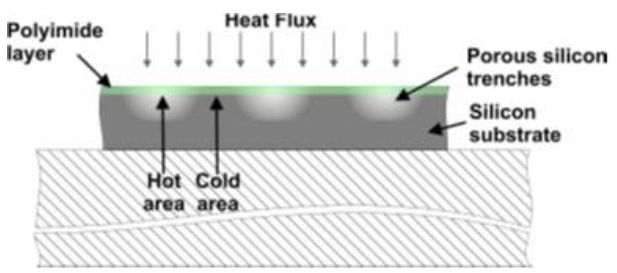
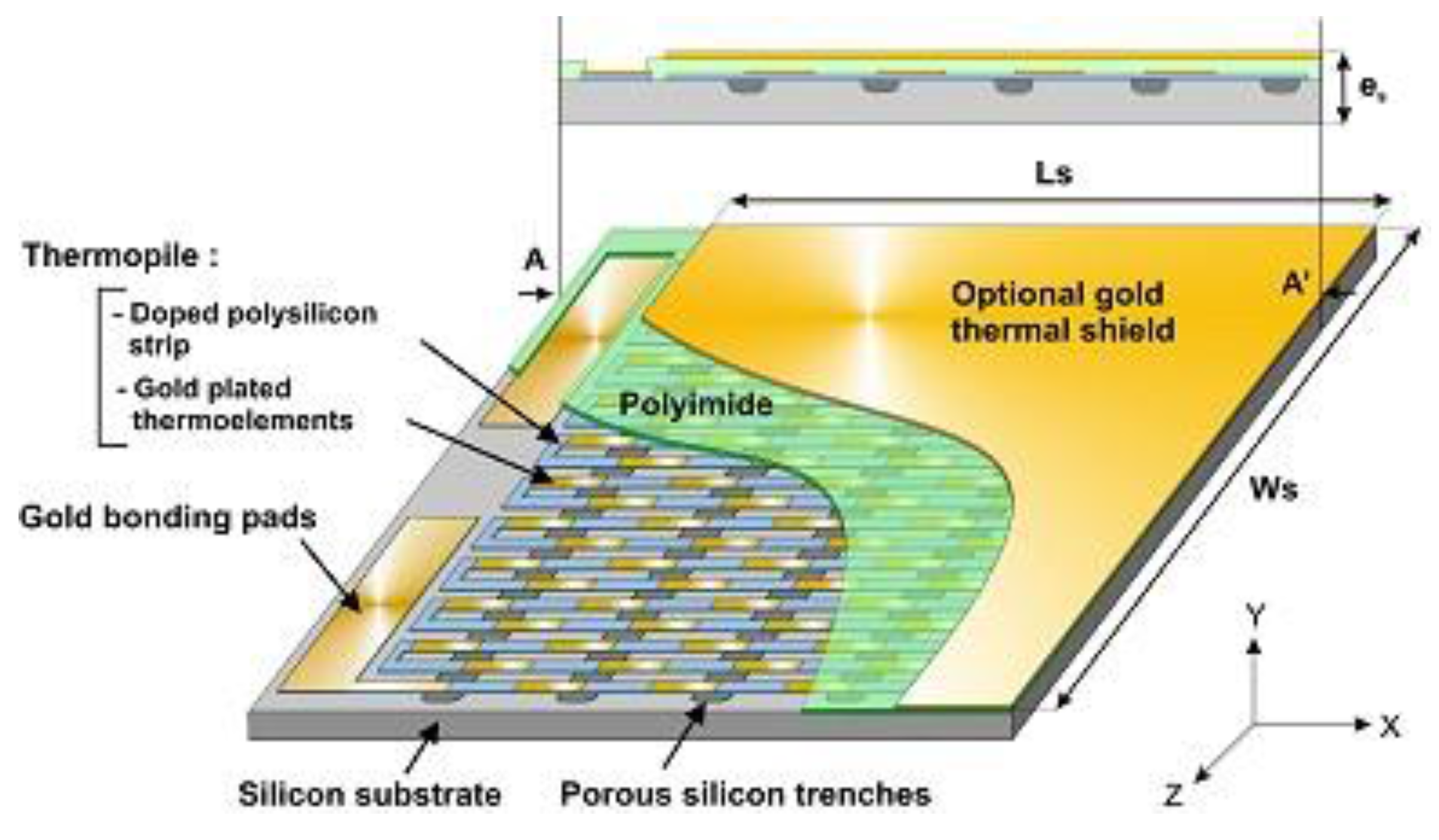
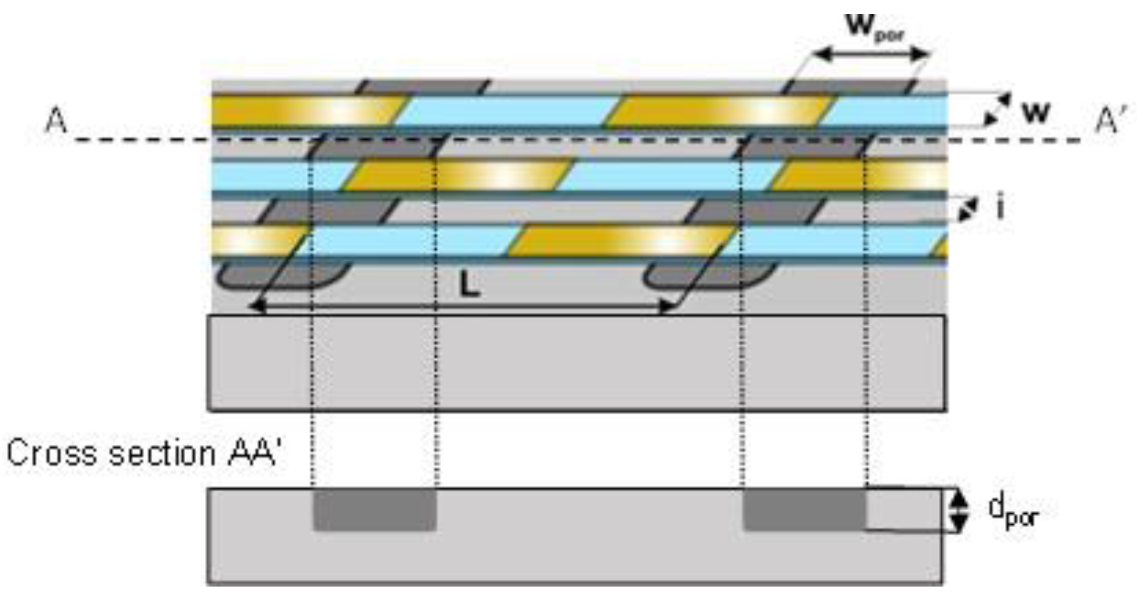
2.1. Sensor Description

The originality of the sensor consists of a thermal asymmetry due to the use of porous silicon trenches in a silicon wafer. Compared to silicon (λSi ~140 W/m·K), porous silicon presents a thermal conductivity 100 times lower (λPorous Si ~1.2 to 2 W/m·K) [11,12,13]. When a transverse heat flux ϕ flows through the sensor, this asymmetry leads to lateral periodic temperature variations ΔT inside the sensor (Figure 1).
A gold/polysilicon thermopile, made of N thermocouples correctly arranged as shown in Figure 2, transforms these gradients of temperature into a Seebeck voltage:
V = N α Δ T
where α (µV/K) is the Seebeck coefficient of the thermocouples.
Assuming the Fourier law [14], a coefficient rth considered as a two-dimensional (2D) thermal resistance between two successive junctions can be expressed by
r th = Δ T φ ( K m 2 / W )
This thermal coefficient is a function of the structural dimensions and thermal conductivities of the different parts and layers constituting the sensor and is determined by using numerical modelling [10]. The sensitivity of the microsensor to a heat flux is given by
S e = dV d φ = N α r th = α A S ( w + i ) r th L ( V m 2 W 1 )
where As is the surface of the sensor, L is the length of a thermocouple, w and i are, respectively, the width of the strips and interstrip of the thermopile (Figure 2).
The electrical resistance Rel of the thermopile which is made of a polysilicon track partially covered by gold strips is
R el = N ( ρ poly L 2 e poly w + ρ poly ρ Au L 2 ( ρ Au e poly + ρ poly e Au ) w )       ( Ω )
with epoly, eAu and ρpoly, ρAu, respectively, the thicknesses and the electrical resistivities for the polysilicon tracks and gold strips.

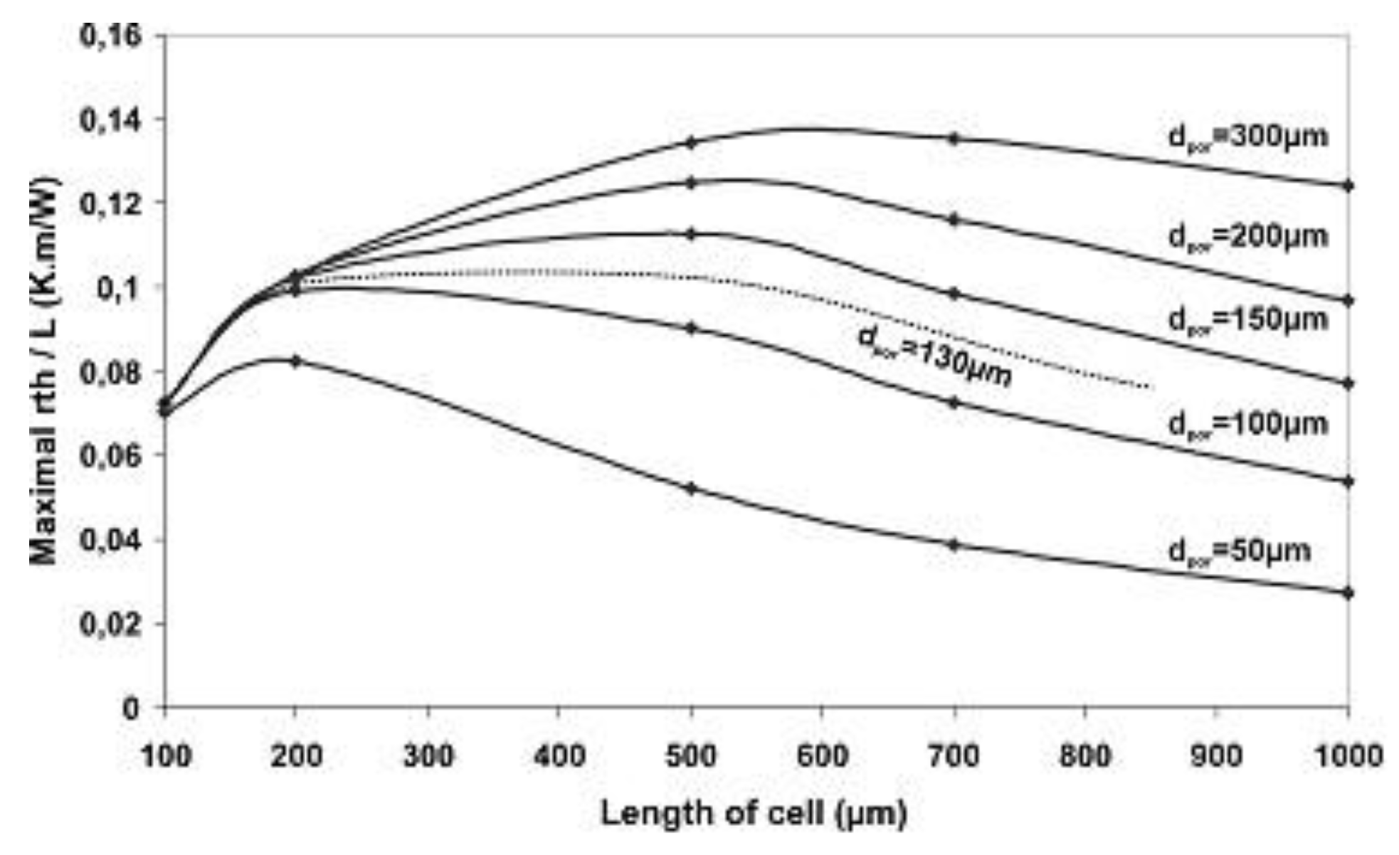
2.2. Thermal Modeling

A numerical model was developed, using COMSOL multiphysics software (COMSOL™ Multiphysics), to optimize the geometrical dimensions of the sensors [10].
As shown in Equation (3), the sensitivity to the heat flux density, Se, is proportional to rth/L. So, to determine the optimal width of the porous trenches wpor according to the thermocouple length L (Figure 3), the evolution of rth/L is studied versus the ratio wpor/L (from 0 to 1) for different values of lengths L (from 100 to 1000 µm) and depths dpor (from 50 to 300 µm). It is demonstrated that the maximum values of rth/L are systematically obtained for the same ratio wpor/L = 0.9, whatever the depth of the porous silicon box and the length of the thermocouple.
In these conditions, the maximum values of rth/L as a function of the cell length L for different depths dpor of porous silicon boxes are represented in Figure 4.
One can observe that the maximum value of rth/L (0.14 K·m/W) that corresponds to an optimal sensitivity, is obtained for L = 500 µm and dpor = 300 µm. In fact, in practice, the depth dpor cannot exceed 150 µm because of the weak mechanical resistance of porous silicon. For a sensor with a width set to 5 mm, the optimum values of the widths of the strips and interstrips of the thermopile are, respectively, w = 80 µm and i = 20 µm. The corresponding polysilicon thickness is epoly = 0.6 μm.
So, to summarize, the geometrical dimensions kept to fabricate the microsensors on a 3-in wafer are: L = 500 µm, epoly = 600 nm, w = 80 µm and i = 20 µm.

3. Experimental Results and Discussion

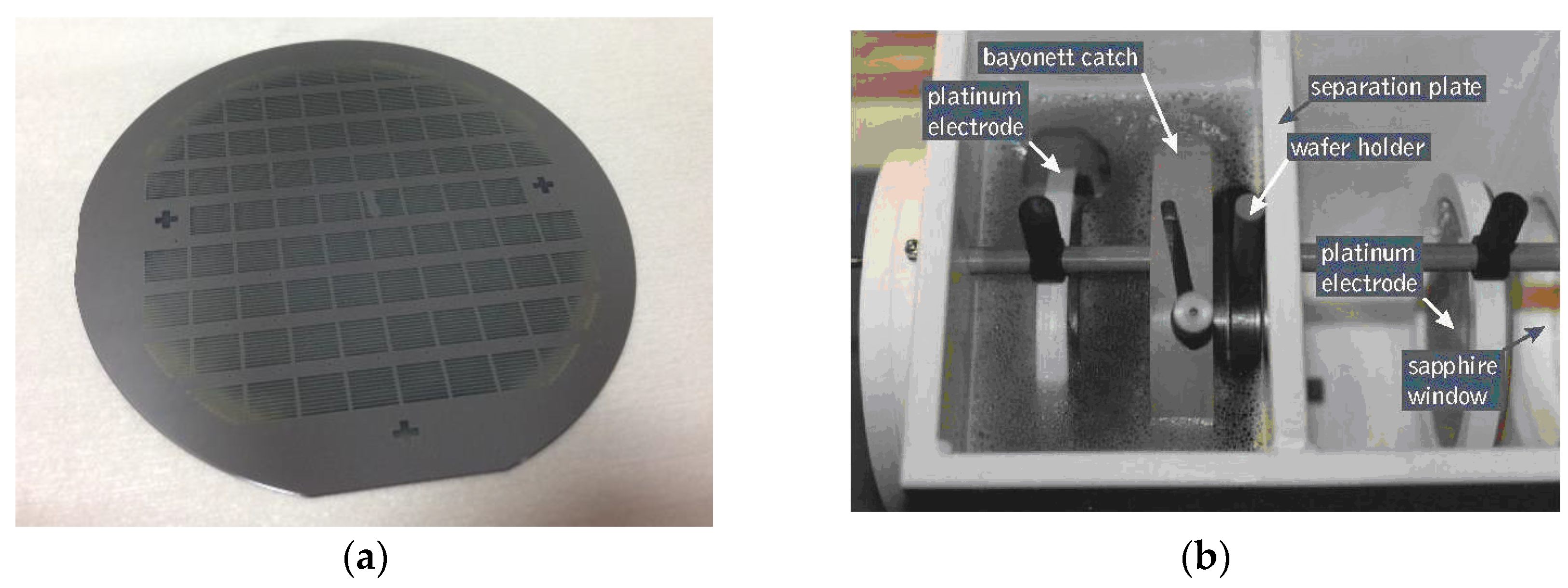
3.1. Sensor Fabrication

The sensitivity Se depends mainly on dpor and wpor (the depth and width of the porous silicon boxes) and on α (the Seebeck coefficient of thermocouples). The electrical resistance Rel depends primarily on the thicknesses epoly, eAu and electrical resistivities ρpoly, ρAu of the polysilicon track and gold strips of the thermoelectric layer (Equation (4)). Thus, these parameters were particularly controlled during the fabrication process. The porous silicon trenches are processed onto 3-in-diameter <100> silicon wafers (thickness is 380 ± 25 µm, p-type doping with Bore and electrical resistivity between 0.009 and 0.01 Ω.cm). The wafers were patterned and anodized (Figure 5a) in a double cell tank (Figure 5b) during several minutes in a mixture of 27% fluorhydric acid (HF), 38% water and 35% ethanol with a current density of 100 mA/cm2 [15].
The engraving speed is approximately 4 to 5 µm per minute. The anodization of silicon lasts about 25 min, resulting in boxes with depths that varies from 100 µm on the center of the wafer to 130 µm on the edges (measured by scanning electron microscopy). These edge effects are mainly due to the dimensions of the wafer (3 in) which are smaller than those of the electrodes (4 inch, Figure 5b). So, the electric lines of current which pass from an electrode to the other one through the wafer undergo a deviation which generates a stronger concentration of the lines in the periphery of the wafer, locally inducing the over-engraving. The polysilicon layer was in situ n-type doped with Phosphorus during its deposition by LPCVD (low pressure chemical vapor deposition). The thermopile zigzag-shaped track was realized by lithography and mesa etching using reactive ion etching with SF6 and CF4 mixture gas. The periodical plated thermoelements were processed by lift-off techniques using the evaporation of a Ti/Au bilayer. The in-plane electrical properties of the polysilicon layer were characterized by Van der Pauw and Hall effect methods. The Seebeck coefficient of the thermocouple was measured on equivalent layers with an experimental set-up [16].
Table 1 presents the range of values for the electrical resistivity ρpoly, thermoelectric coefficient α and thickness epoly of the polysilicon layer measured in different locations of the wafer [16]. The thickness eAu of the Ti/Au bilayer is 250 nm ± 10 nm. Because of its very low electrical resistivity, this layer has a minor impact on the value of the electrical resistance of the thermopile (Equation (4)).

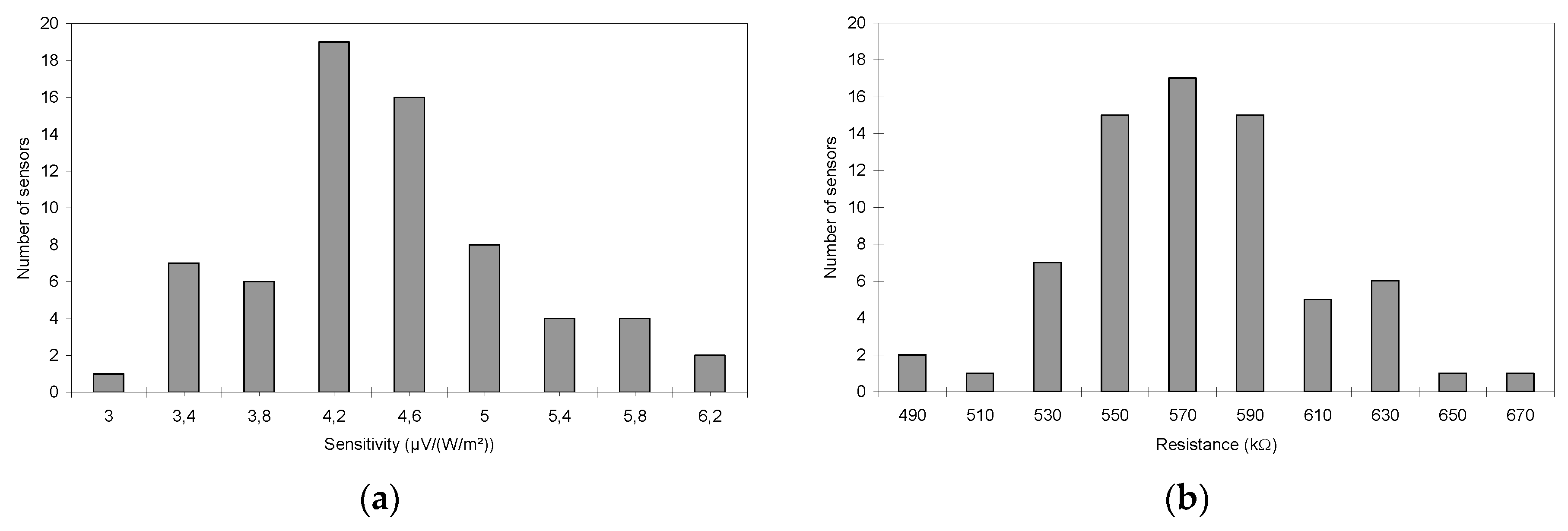
3.2. Sensor Characterizations

A set of five masks was used for the fabrication of the sensors on a complete 3-in wafer. First of all, the positions of the efficient heat flux sensors on the wafer were established. Then, the sensitivities and electrical resistances of the 74 efficient sensors were measured: the values are given in Table 2. The sensitivities Se of the heat flux sensors were determined by the radiative method. The calibration is described in [10]. These sensors do not need cooling. They can operate from ambient temperature up to 200 °C.
A first analysis of these results shows that, for the four sensors situated at the four corners of Table 2 (nbr 1, nbr 6, nbr 69 and nbr 74), the sensitivity Se is very low because of incomplete porous silicon boxes, as shown in Figure 5a. This is caused by the mark left by the seal glued onto the wafer during the electrolysis. The seal is used to isolate the electrolytes of the two tanks in order to avoid electric current leaks. One can also find a few other low values of electrical resistances that are due to contacts resulting in shunts between two adjacent strips of the thermopile (nbr 44, nbr 52 and nbr 65). These kinds of problems can occur during different steps in the fabrication process: lithography, polysilicon engraving or lift-off of the Ti/Au layer which is the second material of the thermopile. We can mention here the challenge of fabricating 500 strips that are 5 mm long and spaced 20 µm apart.
When only considering the 67 reliable sensors, one finds that the measured sensitivities vary between 3.15 and 6.56 µV/(W/m2) and, that the measured resistance values lie between 485 and 675 kΩ. The average values of sensitivity and electrical resistance are respectively S e ¯   = 4.5 µV/(W/m2) and R ¯ = 573.5 kΩ. The global dispersions of both parameters are given in Figure 6. The two histograms exhibit Gaussian-type distributions. From these results the calculated standard deviations are, respectively, σSe = 0.74 µV/(W/m2) and σR = 34.8 kΩ. Furthermore, 95.6% of the sensitivity values are within the interval [ S e ¯   − 2σSe; S e ¯   + 2 σSe] and 73.5% in [ S e ¯   − σSe; S e ¯   + σSe]. Similarly, 94.3% of the resistances are in the range [ R ¯ − 2σR; R ¯ + 2σR] and 74.3% in [ R ¯ − σR; R ¯ + σR].

3.3. Discussion

As stated before the depth of the porous silicon boxes dpor is between 100 µm and 130 µm. The corresponding thermal coefficient rth is deduced from numerical model curves (Figure 4) and the ratio rth/L lies between 0.088 and 0.101 K·m/W.
By introducing these values of rth/L and the thermoelectric coefficient α given in Table 1 in Equation (3), the calculated sensitivity can be evaluated between 4.84 and 6.57 µV/(W/m2). So the calculated sensitivity range cross the experimental range [   S e ¯   − σSe; S e ¯   + σSe] (i.e., 3.76–5.24 µV/(W/m2)) and encompass the experimental average value (4.5 µV/(W/m2)). There is a slight shift in the measured values.
In the same way, the electrical resistances are calculated by using Equation (4). The contact resistances between the polysilicon layer and the (Ti/Au) bilayer are measured by the transmission line method (TLM) and the Van Der Pauw method. It is approximately 7 Ω for each thermocouple, corresponding to few kΩ for the sensor, and it can therefore be neglected. Consequently, with the minimal and maximal values of ρpoly and epoly given in Table 1, the theoretical values of the total resistance vary between 517 and 658 kΩ. The comparison to the measured values, which range between 538.7 and 608.3 kΩ (average value of 573.5 kΩ), is quite good.
The good agreement observed between the theoretical and measured values demonstrates the performance and the reliability of the fabrication process. Actually the electrical resistances and sensitivities of the sensors are higher at the periphery of the wafer. The values of the sensitivities are explained by the greater thickness of the porous silicon boxes and the higher thermoelectric power at this location of the wafer. A lower sensitivity for some peripheral sensors is due to an incomplete manufacturing of the corresponding porous silicon boxes. Concerning the values of the electrical resistances, the variations are essentially due to a local lower thickness of the polysilicon and to a higher resistivity.

4. Conclusions

In this paper, a study of the performance and reliability of heat flux microsensors fabricated by means of technological processes and equipment suited to 3-in wafers has been proposed. In particular, we show that the dispersion observed in terms of sensitivity and electrical resistance is closely related to the limits of the equipment and of the processes used. Actually, the 3-in processes do not allow obtaining homogeneous coats on 3-in wafers (two sizes above needed). The LPCVD technique allows achieving a thickness of polysilicon with fluctuations of about ±5%. The resistivity and the thermoepower bound to the doping level are not homogeneous, with fluctuations of about ±8%. A doping by implanting should allow a better homogeneity than the doping in situ. The anodization process entails a difference in the thickness of porous silicon between the center and the periphery of the wafer which is translated to a difference in sensitivity of 10%. This value can be reduced by increasing the distance separating the electrodes of the wafer.Finally, it has been shown that differences between the values of sensors’ sensitivities in the periphery of the wafer are mainly due to edge effects. If we consider the results obtained for the sensors located in an area of about 2-in in diameter centred on the wafer, the dispersion is much better: with 80% of the sensitivities within the interval S e ¯ -Se; S e ¯ + 2σSe where Se = 4.46 µW/(W/m2) and σSe = 0.44 µW/(W/m2). These results altogether highlight the reliability and maturity of the technology process. The heat flux microsensors are therefore a viable solution for applications outside a laboratory environment.

Acknowledgments

This work was supported by “Bpifrance” in the frame of the “Open Food System Project”. It was also partly supported by the French RENATECH network.

Author Contributions

K. Ziouche and D. Leclercq conceived and designed the experiments; K. Ziouche and P. Lejeune performed the experiments; K. Ziouche and Z. Bougrioua contribute the materials and analysis tools; all the authors analyzed the data and wrote the manuscript.

Conflicts of Interest

The authors declare no conflict of interest.

References

  1. Lenggenhager, R.; Baltes, H.; Elbel, T. Thermoelectric infrared sensors in CMOS technology. Sens. Actuators A Phys. 1993, 14, 216–220. [Google Scholar] [CrossRef]
  2. Sion, C.; Godts, P.; Ziouche, K.; Bougrioua, Z.; Lasri, T.; Leclercq, D. Unpackaged infrared thermoelectric microsensor realized on suspended membrane by silicon technology. Sens. Actuators A Phys. 2012, 175, 78–86. [Google Scholar] [CrossRef]
  3. Zhou, H.; Kropelnicki, P.; Tsai, J.M.; Lee, C. Development of a thermopile infrared sensor using stacked double polycrystalline silicon layers based on the CMOS process. J. Micromech. Microeng. 2013. [Google Scholar] [CrossRef]
  4. Boutchich, M.; Ziouche, K.; Ait-Hammouda Yala, M.; Godts, P.; Leclercq, D. Package free infrared microsensor using thermopile. Sens. Actuators A Phys. 2005, 121, 52–58. [Google Scholar] [CrossRef]
  5. De Vrient, A.B. La Transmission de la Chaleur, 3rd ed.; Morin, G., Ed.; Boucherville, QC, Canada, 1992; Volume 2. [Google Scholar]
  6. Ziouche, K.; Godts, P.; Leclercq, D. Polyimid resist as infrared absorbing layer for radiation microsensors. Sens. Mater. 2000, 12, 445–454. [Google Scholar]
  7. Ziouche, K.; Boutchich, M.; Bernard, D.; Godts, P.; Leclercq, D. A New Ultra-Violet Microradiometer. In Proceedings of the International Frequency Sensor Association, Nuremberg, Germany, 9 May 2001.
  8. Godts, P.; Dupont, D.; Leclercq, D. Direct measurement of the latent heat of evaporation by flowmetric method. IEEE Trans. Instrum. Meas. 2005, 54, 2364–2369. [Google Scholar] [CrossRef]
  9. Mancier, V.; Leclercq, D. Power dissipated measurement of an ultrasonic generator in a viscous medium by flowmetric method. Ultrason. Sonochem. 2008, 15, 973–980. [Google Scholar] [CrossRef] [PubMed]
  10. Ziouche, K.; Godts, P.; Bougrioua, Z.; Sion, C.; Lasri, T.; Leclercq, D. Quasi-monolithic heat-flux microsensor based on porous silicon boxes. Sens. Actuators A Phys. 2010, 164, 35–40. [Google Scholar] [CrossRef]
  11. Drost, A.; Steiner, P.; Moser, H.; Lang, W. Thermal conductivity of porous silicon. Sens. Mater. 1995, 7, 111–120. [Google Scholar]
  12. Benedetto, G.; Boarino, L.; Brunetto, N.; Rossi, A.; Spagnolo, R.; Amato, G. Thermal properties of porous silicon layers. Philos. Mag. Part B 1997, 76, 383–393. [Google Scholar] [CrossRef]
  13. Ziouche, K.; Bougrioua, Z.; Lejeune, P.; Lasri, T.; Leclercq, D. Probing Technique for Localized Thermal Conductivity Measurement. Meas. Sci. Technol. 2015. [Google Scholar] [CrossRef]
  14. Özisik, M.N. Heat Conduction; John Wiley and Sons: New York, NY, USA, 1993. [Google Scholar]
  15. Lysenko, V.; Roussel, P.; Remaki, B.; Delhomme, G.; Dittmar, A.; Barbier, D.; Martelet, C.; Strikha, V.; Boarino, L.; Bertola, M.; et al. Formation of thick oxidized meso porous silicon layers with low thermal conductivity for thermal isolation applications. In Proceedings of the Therminic’98, International Workshop on Thermal Investigations of IC’s and Microstructures, Cannes, France, 28 September 1998; pp. 51–56.
  16. Boutchich, M.; Ziouche, K.; Godts, P.; Leclercq, D. Characterization of Phosphorus and Boron Heavily. IEEE Electron Device Lett. 2002, 23, 139–141. [Google Scholar] [CrossRef]
Figure 1. Cross-sectional view of periodic temperature variations induced by the heat flux.
Sensors 16 00853 g001
Figure 2. Schematic diagram of the heat flux microsensor.
Sensors 16 00853 g002
Figure 3. Zoom on an elementary cell of the heat flux microsensor.
Sensors 16 00853 g003
Figure 4. Values of rth/L versus cell length for different depths of porous silicon trenches for wpor/L = 0.9.
Sensors 16 00853 g004
Figure 5. (a) Photography of a 3-in-diameter silicon wafer with processed porous silicon trenches; (b) Double cell HF tank for porous silicon etching with electrolytic backside contact (AMMT).
Sensors 16 00853 g005
Figure 6. Dispersion histograms of (a) sensitivities; and (b) resistances.
Sensors 16 00853 g006
Table 1. Range of values for electrical resistivity ρpoly, thermoelectric coefficient α and thickness epoly of the polysilicon layer.
ρpoly (mΩ·cm)α (µV/K) at 298 Kepoly (nm)
Dispersion0.0205–0.024220–260570–620
Table 2. Sensors’ sensitivities and electrical resistances measured on a complete 3 in wafer.
Column12345678910
Ligne
1Sensor number 123456
R (kΩ) 637570580675570557
Se (µV/(W/m²)) 23.93.393.93.232.02
2Sensor number 7891011121314
R (kΩ) 548560570570589657620584
Se (µV/(W/m²)) 4.593.475.444.54.24.153.443.32
3Sensor number15161718192021222324
R (kΩ)577573571569590550530588625597
Se (µV/(W/m²))3.545.733.973.913.8644.54.634.763.24
4Sensor number252627282930313233-
R (kΩ)547570550538620570565612590
Se (µV/(W/m²))6.465.34.784.123.94.174.124.34.46
5Sensor number 3435363738394041
R (kΩ) 552435530545490573580620
Se (µV/(W/m²)) 6.134.34.454.14.124.294.645.24
6Sensor number42434445464748495051
R (kΩ)537535278554535525485596604620
Se (µV/(W/m²))6.565.572.354.544.194.234.24.234.496.02
7Sensor number52535455565758596061
R (kΩ)136556556564531546555606588585
Se (µV/(W/m²))35.574.564.384.14.154.534.354.945
8Sensor number 62636465666768-
R (kΩ) 550575561350585585605
Se (µV/(W/m²)) 5.844.494.492.84.94.94.24
9Sensor number 697071727374
R (kΩ) 557516574584598600
Se (µV/(W/m²)) 2.355.75.25.24.521.57

