1. Introduction
Si-based photonic devices have experienced tremendous progress in recent years [
1,
2,
3] and a large scale fabrication of photonic and combined photonic-electronic integrated circuits (PEICs) show a strong uptrend in developing markets like datacom, telecommunication, and sensing [
4,
5,
6,
7,
8,
9].
Hydrogenated amorphous silicon (a-Si:H) is, in particular, a promising platform enabling the desired matching between electronics and on-chip photonics [
10]. In a back-end approach, thin layers of a-Si:H can be in fact deposited on top of electronic microchips using the CMOS-compatible low-temperature plasma-enhanced chemical vapor deposition (LT-PECVD) technique, with no impact at all on the underlaying microelectronic circuit. a-Si:H can be also deposited on different substrates where crystalline silicon (c-Si) could not, be it a glass, a metal, an already processed silicon (Si) wafer, or even plastic.
However, many fabricated microelectronic or photonic integrated devices are very sensitive to external variations including temperature, bias voltage, and working wavelengths. In particular, Si-photonic active devices are strongly temperature-dependent, namely they are sensible to the environment temperature modifications due to the large thermo-optic (TO) coefficient of Si [
11]. In the last decades, the refractive index temperature dependence has been modeled analytically and the Si TO coefficient has been related to the variation of the inter-band transition energies at some critical points of the Si band structure [
12]. Moreover, it has been shown that the TO coefficient of a-Si:H is slightly higher than that of c-Si, resulting, respectively,
dn/dT = 2.3 × 10
−4 K
−1 [
13] and
dn/dT = 1.8 × 10
−4 K
−1 [
12] at the wavelength of 1550 nm at T = 300 K, which might diminish in part the advantages brought by the easy and low cost technology of a-Si:H.
As anticipated, in fact, refractive index variation with temperature can determine a non-correct behavior of integrated active devices such as interferometers, modulators, photodiodes, sensors. Therefore, thermal challenges need to be resolved in order to advance the silicon photonics to its final industrial stage. For example, the thermal sensitivity of the resonant wavelength for Si-based ring resonators is, e.g., approximately 100 pm/°C [
14] or, to mention another example, in a Mach Zehnder (MZ) interferometer the TO effect is responsible of a wavelength shift of 90 pm/°C [
15]. In Vernier effect-based photonic sensors, the microchip must be thermally stabilized to prevent the drift of the sensor output signal [
16]. Consequently, the temperature-dependent optical performance of an on-chip integrated photonic device is a real issue to be taken into account during the design of PEICs [
17], and these devices are not practical without a continuous thermal compensation during their operating life.
Recently, on-chip temperature measurement has been proposed for thermal variation compensation in many sensing devices such as humidity, pressure, flow, stress and gas concentration sensors [
18].
Among different types of integrated temperature-sensing devices, the advantage of diode-based temperature sensors is the compatibility with IC technology, the low manufacturing costs, the quasi-linear output voltage-temperature,
VD-T, behavior while preserving a high sensitivity [
19].
When a diode operates as a temperature sensor, it is forward-biased at a current
ID kept constant over the whole temperature working range and the corresponding voltage drop
VD allows an accurate indirect temperature measurement. Low values of bias currents reduce device self-heating and the negative effects of the parasitic series resistance among which are a poorer linearity and sensitivity [
20].
In the last years, few examples of a-Si:H p-i-n diode have been proposed as temperature sensor in a temperature range from
T = 30 °C up to 90 °C. The devices showed a good linearity and a sensitivity of 3.2 mV/°C for a DC bias current of 10 nA [
21].
In this work, a temperature sensor based on an a-Si:H p-i-n diode integrated in photonic layer is presented in detail. The sensor is placed very close to a MZ electro-optic modulator in order to monitor the chip temperature variations. The linear dependence of the voltage drop across the forward-biased diode on temperature from T = 30 °C up to 170 °C has been accurately measured.
2. Device Structure
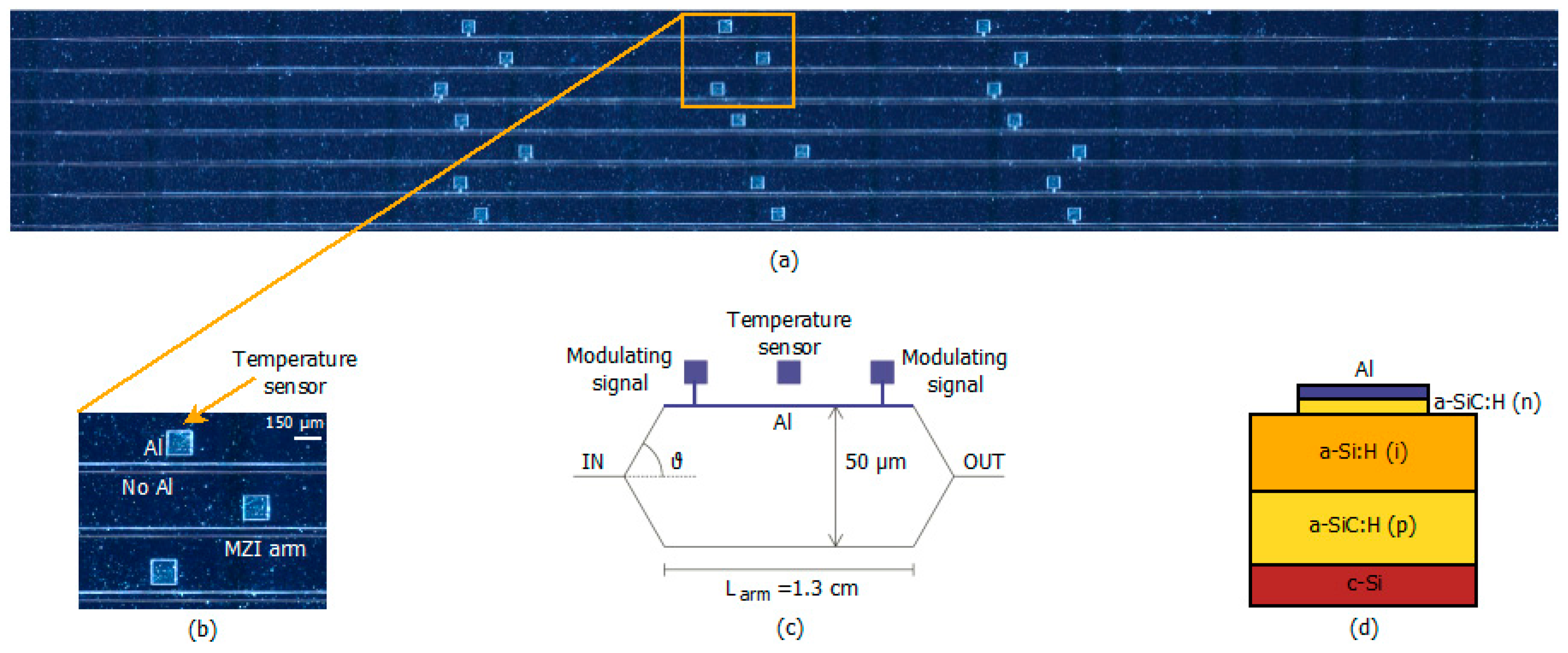
The diode temperature sensor was integrated in the proximity to a Mach Zehnder interferometer (MZI),
Figure 1a,b, and in particular close to the MZI arm where the propagating optical signal is phase shifted by carrier depletion induced in turn by the electric-field applied across the p-i-n diode. The schematic layout of the realized device is shown in
Figure 1c together with its geometrical dimensions. More details about the MZI fabrication and operation are provided in [
22,
23].
The schematic cross section of the fabricated a-Si:H waveguide, integrating the vertical p-i-n diode is shown
Figure 1d. It consists of an intrinsic a-Si:H layer, 2-μm-thick, between a p-doped a-SiC:H, 2-μm-thick, and an n-doped a-SiC:H, 300-nm-thick. The p-i-n cathode top contact is a 200-nm-thick Al layer. The active area of the device is 2.25 × 10
−4 cm
2.
As well-known, the
ID current flowing in a p-i-n diode at a given applied voltage
VD can be analytically described using the following formula:
where
η is the ideality factor,
Is is the saturation current,
q is the electric charge and
k is the Boltzmann constant.
The characterization of the sensor output has been performed under forward bias condition where, at constant DC current, the voltage across the diode is linearly dependent on the temperature.
In fact, for
q∙VD>> η
∙k∙T, the voltage dependence on temperature can be obtained from Equation (1), yielding:
Equation (2) makes explicit the linear dependence
VD-T as long as the non-linear contribution of
Is can be considered negligible with respect to
ID [
24,
25].
Figure 1.
(a) An optical microscope image (top view) of the a-Si:H-based MZI modulators and temperature sensors; (b) temperature sensor detail; (c) schematic MZI and temperature sensor (plot not in scale); and (d) cross section of the integrated a-Si:H p-i-n diode temperature sensor.
Figure 1.
(a) An optical microscope image (top view) of the a-Si:H-based MZI modulators and temperature sensors; (b) temperature sensor detail; (c) schematic MZI and temperature sensor (plot not in scale); and (d) cross section of the integrated a-Si:H p-i-n diode temperature sensor.
3. Experimental Results and Discussion
In our setup, the p-i-n diodes were biased with a current
ID kept constant in the whole temperature range. The devices were tested in a climatic chamber (Galli Genviro-030-C) setting the reference temperature through its internal PID digital microcontroller. A calibrated PT100 sensor, with an accuracy of ±0.3 °C, was placed in contact with the device under test in order to monitor, during the measurements, the exact temperature set points gradually varied from (to) 30 °C to (from) 170 °C. By using an Agilent 4155C semiconductor parameter analyzer, tests were made for
ID varied in a range from 1 nA to 80 nA (±100 pA accuracy and 10 pA resolution, for generated currents in the range −100 nA <
ID < 100 nA) and the corresponding voltage drop
VD across the a-Si:H p-i-n diode was measured. In
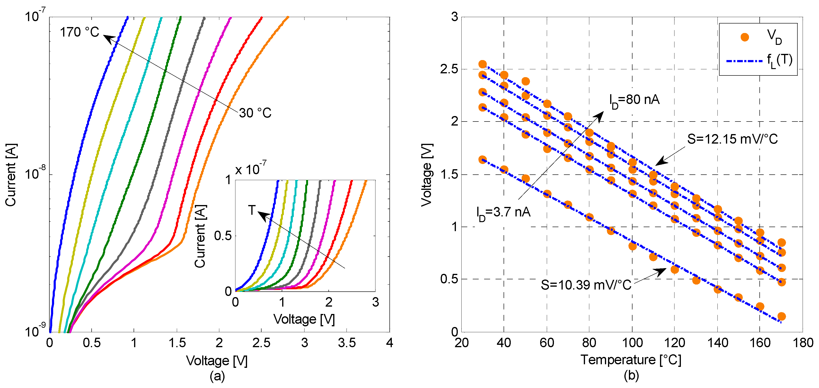
Figure 2a we report the
ID-VD characteristics, for different temperatures in a range from 30 °C up to 170 °C.
From
ID-VD-T measurements, a highly linear behavior of the voltage drop across the p-i-n diode on different temperatures was extracted, as shown in
Figure 2b.
In our analysis, the coefficient of determination
(R2) [
26] has been calculated to evaluate the agreement between the experimental measurements and their linear best-fit,
fL(T). In particular,
R2 allowed us to quantify the sensor linearity goodness by fitting the experimental data with a linear model.
In the same figure, the measured data are fitted with the best-calculated linear model showing a good degree of linearity (R2 > 0.995) for the whole considered range of ID, 3.7 nA to 80 nA.
The sensor sensitivity, S, is defined as the temperature derivative of Equation (2) and, therefore, it can be calculated from the slope of the VD-T characteristics.
As reported in
Figure 2b, when
ID is 3.7 nA the sensitivity is 10.39 mV/°C and increases up to 12.15 mV/°C for
ID = 80 nA.
Figure 2.
(a) Forward current-voltage characteristics for temperatures ranging from 30 °C up to 170 °C, with ΔT = 20 °C steps. The inset shows a detail of the ID-VD characteristics in linear scale. (b) Measured (points) forward voltages versus temperature at different bias currents (ID = 3.7, 22.8, 37.3, 60.4, 80 nA). Experimental data are fitted with the best-calculated linear model fL(T).
A more detailed analysis of
R2 and
S is shown in
Figure 3a,b for all values of
ID in steps of 100 pA.
It is worth noting that the coefficient of determination varies by only 0.25% from an average of Ra2 = 0.9972 over the considered temperature range leading to a temperature sensor with a highly linear behavior in a wide range of biasing currents. The maximum of R2 = 0.9996 occurs in the current range ≈ 34–40 nA. Within this current range, the sensitivity is constant, S = 11.93 mV/°C.
To evaluate the mismatch between the calculated linear best-fit,
fL(T), and the experimental measurements, the corresponding root mean square error
(rmse) was first calculated and subsequently converted into a temperature error value using the following formula:
where
n is the number of the temperature set points.
The calculated plot,
rmse versus ID, for the considered temperature range is reported in
Figure 3c. The temperature error is always lower than 3.5 °C, while the minimum
rmse = 0.89 ± 0.01 °C is obtained for
ID = 37.3 ± 3.3 nA.
It is worth noting that the current source accuracy of ±100 pA falls within the above reported range of
ID for which the
rmse and the sensitivity remain almost constant with no impact on the sensor performances. In practical applications, if we consider that the proposed device is intended for integration on a VLSI electronic microchip, the well-known technics for current stabilization based on bandgap references and current mirrors circuits could be used in association [
27].
The temperature resolution, ε
T, of a sensor measuring a temperature
T is limited by the measurement system resolution, ε
V, according to the expression:
when the sensitivity of the sensor,
S = dV/dT, does not change significantly within the considered temperature range. In our experimental setup, the measured voltage resolution is 20 µV leading to a theoretical device resolution of 1.7 m°C.
The large sensitivity allows in principle the resolution of small temperature variations, however, the smallest detectable temperature change is limited by several error sources including sensor and measurement system calibration, bias current and measured voltage accuracy, noise, sensor self-heating, etc.
The specific applications our integrated a-Si:H sensor is intended for, require however temperature measurements with an accuracy of the order of ±1 °C about.
In fact, if we consider, e.g., the wavelength division multiplexing (WDM) technique for fiber-optic communications, in which multiple optical signal channels are carried by a single fiber at different wavelengths of light, the spacing between two adjacent wavelengths is not smaller than Δλ~1 nm. In particular, for coarse wavelength division multiplexing (CWDM) is about Δλ = 10–20 nm, while in dense wavelength division multiplexing (DWDM) the spacing is about 0.8 to 2 nm [
28]. Due to the tight spacing, DWDM systems require elaborate temperature control systems to ensure that the optical channels do not interfere each other.
Figure 3.
(a) Sensitivity, S; (b) coefficient of determination, R2; and (c) root mean square error, rmse, for the whole temperature range of 30–170 °C for bias currents between ID = 3.7–80 nA.
Figure 3.
(a) Sensitivity, S; (b) coefficient of determination, R2; and (c) root mean square error, rmse, for the whole temperature range of 30–170 °C for bias currents between ID = 3.7–80 nA.
As already mentioned, for actual Si-based integrated active photonic devices, the wavelength shift, due to the temperature change, does not exceed ~100 pm/°C [
14,
15], and therefore temperature measurements with resolution and accuracy of the order of a few tenths of a degree Celsius match the specifications of any practical control system.
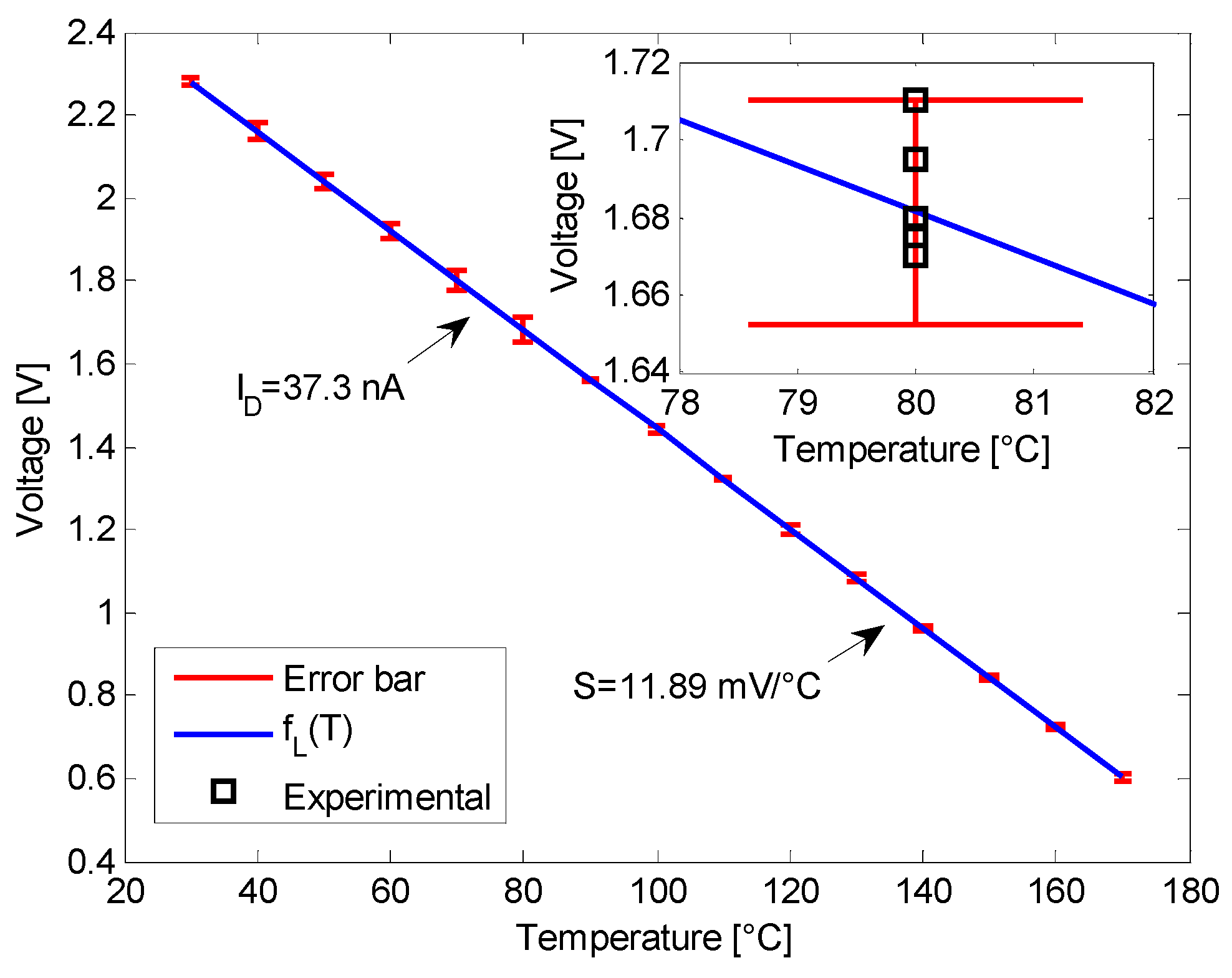
The sensor precision, in term of stability and reproducibility, is a measure of how closely all the measured and calculated data are grouped around the characteristic mean values. In our analysis, the a-Si:H integrated temperature sensor was therefore accurately tested in order to evaluate how consistently it maintains a stable output over time by iteratively repeating three cycles of measurements, from (up to) 30 °C up to (from) 170 °C, in a long period of time and for five different diodes fabricated with the same process.
The results are summarized in
Figure 4, for
ID = 37.3 nA, and leaded to a calculated maximum
rms error lower than ±1.7%. Moreover, the coefficient of determination is
R2 = 0.9993 ± 3 × 10
−4 and the corresponding sensitivity is
S = 11.89 mV/°C with a standard deviation of 0.08 mV/°C.
Figure 4.
Linear fit and rmse of VD vs. T for five different diodes fabricated with the same technological process and measured in a long period of time. The measurement cycles, from (up to) 30 °C up to (from) 170 °C, were done in different days. The bias current is ID = 37.3 nA for all five sensors. The inset shows the distribution of VD for the five different diodes at T = 80 °C.
In the inset of
Figure 4, the measured voltage drops on the five characterized diodes are shown at the temperature of 80 °C, where the scattering is maximum.
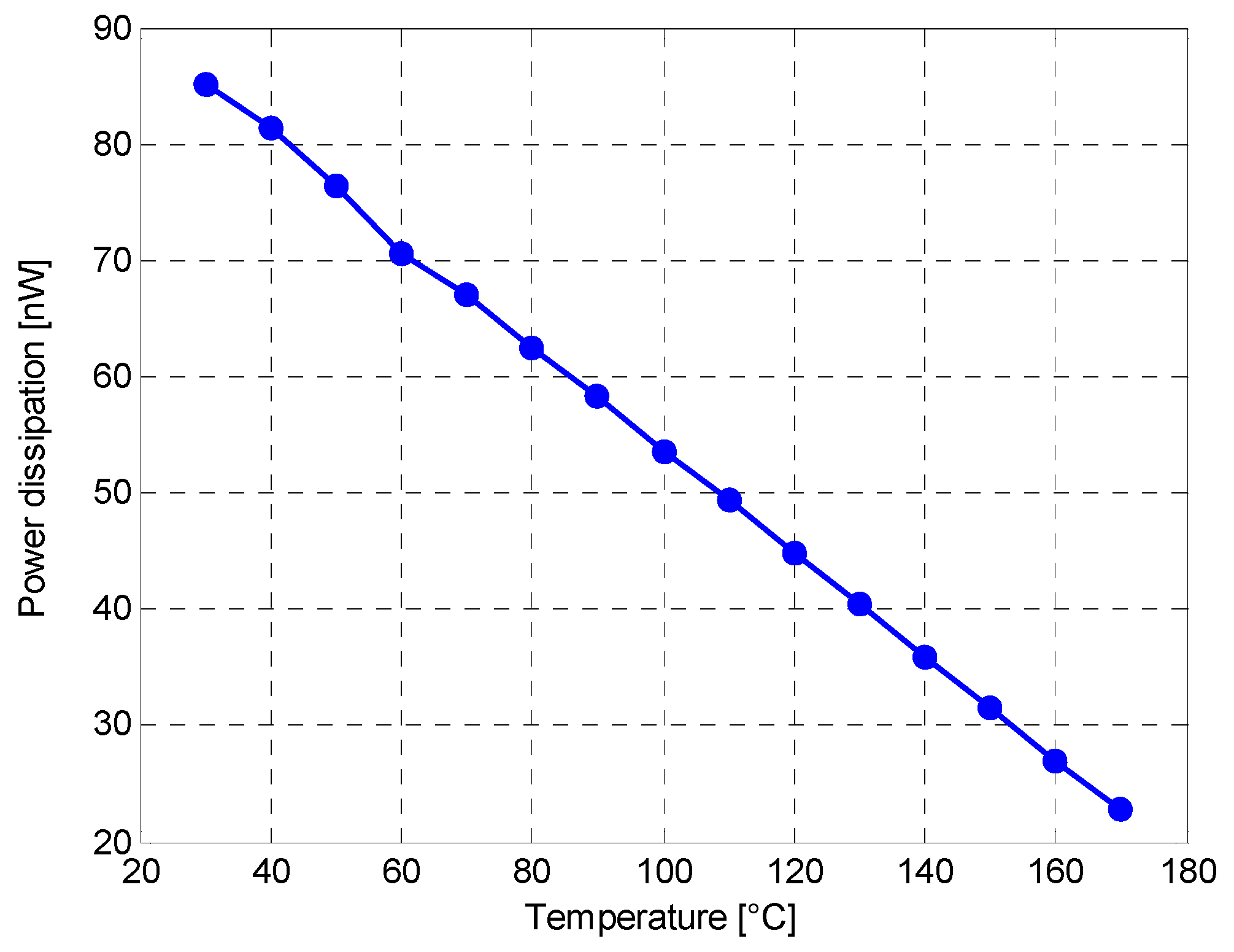
In
Figure 5 is shown the power dissipation (
PD) of the a-Si:H temperature sensor, for
ID = 37.3 nA, in the considered temperature range. The calculated values decrease with temperature with a maximum
PD of ~85 nW at 30 °C, low enough to avoid device self-heating.
Figure 5.
Power dissipation vs. temperature characteristics for ID = 37.3 nA.
Figure 5.
Power dissipation vs. temperature characteristics for ID = 37.3 nA.


