
Electronic Properties of DNA-Based Schottky Barrier Diodes in Response to Alpha Particles

Abstract
:1. Introduction
2. Methodology
2.1. Preparation of DNA Solution
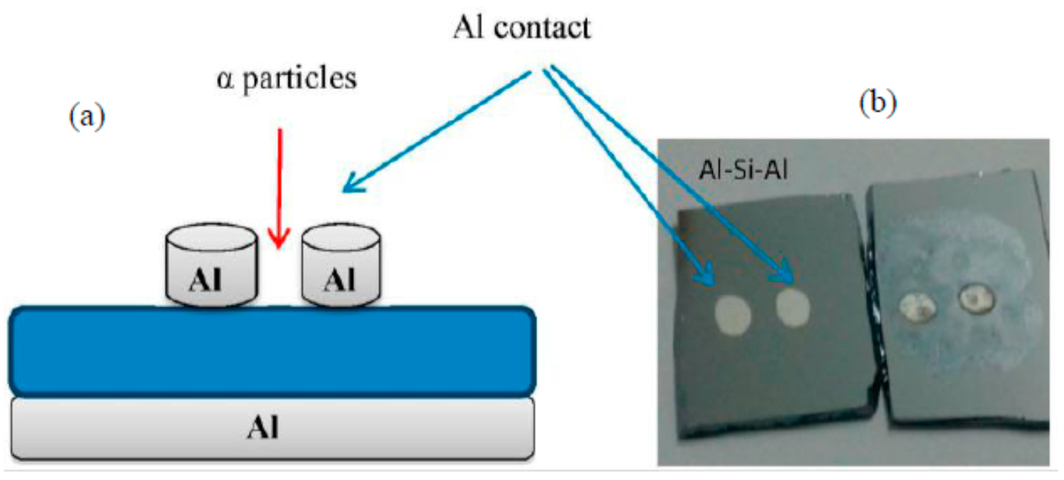
2.2. Preparation of Al/DNA/p-Si/Al Junctions

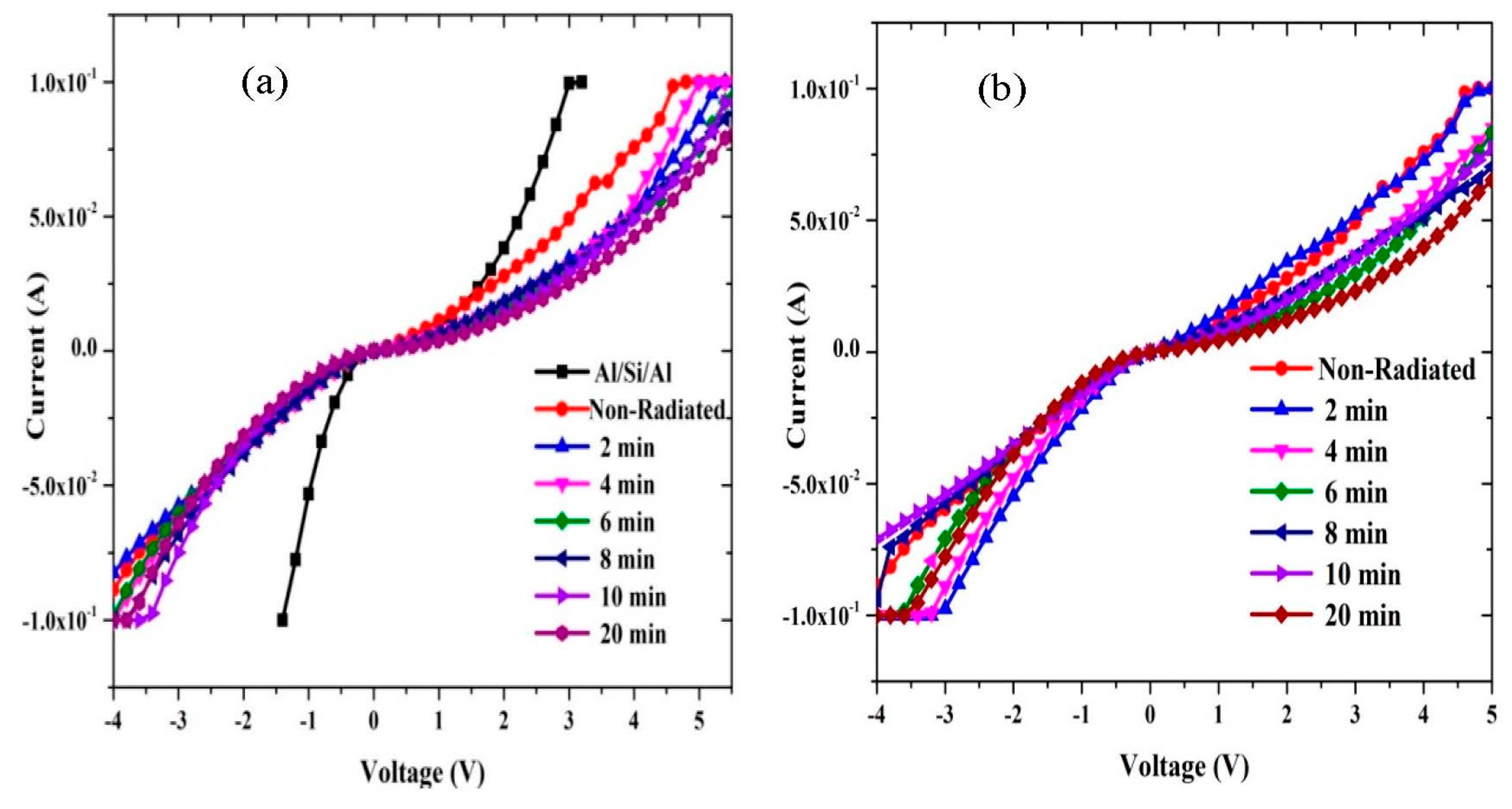
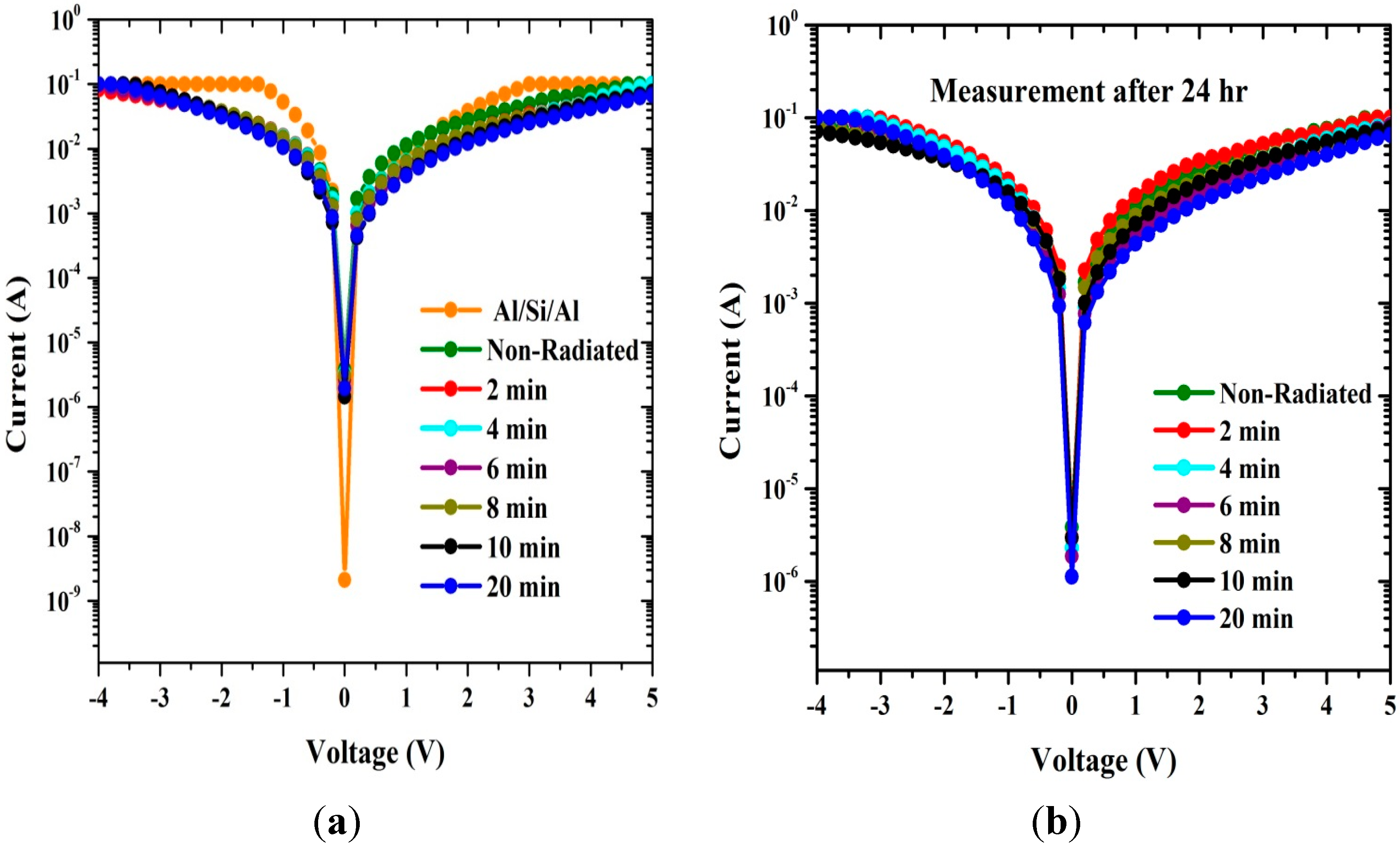
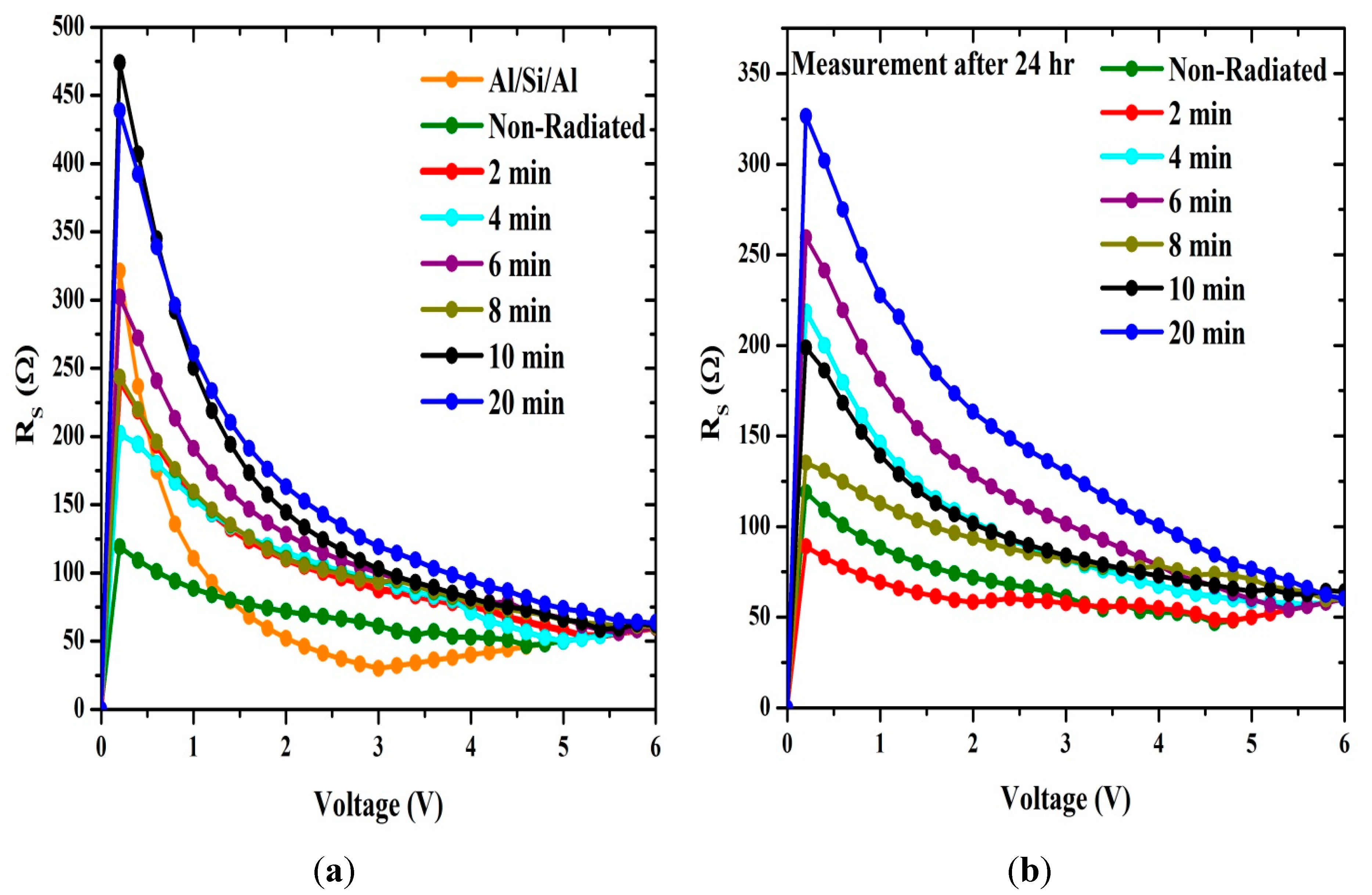
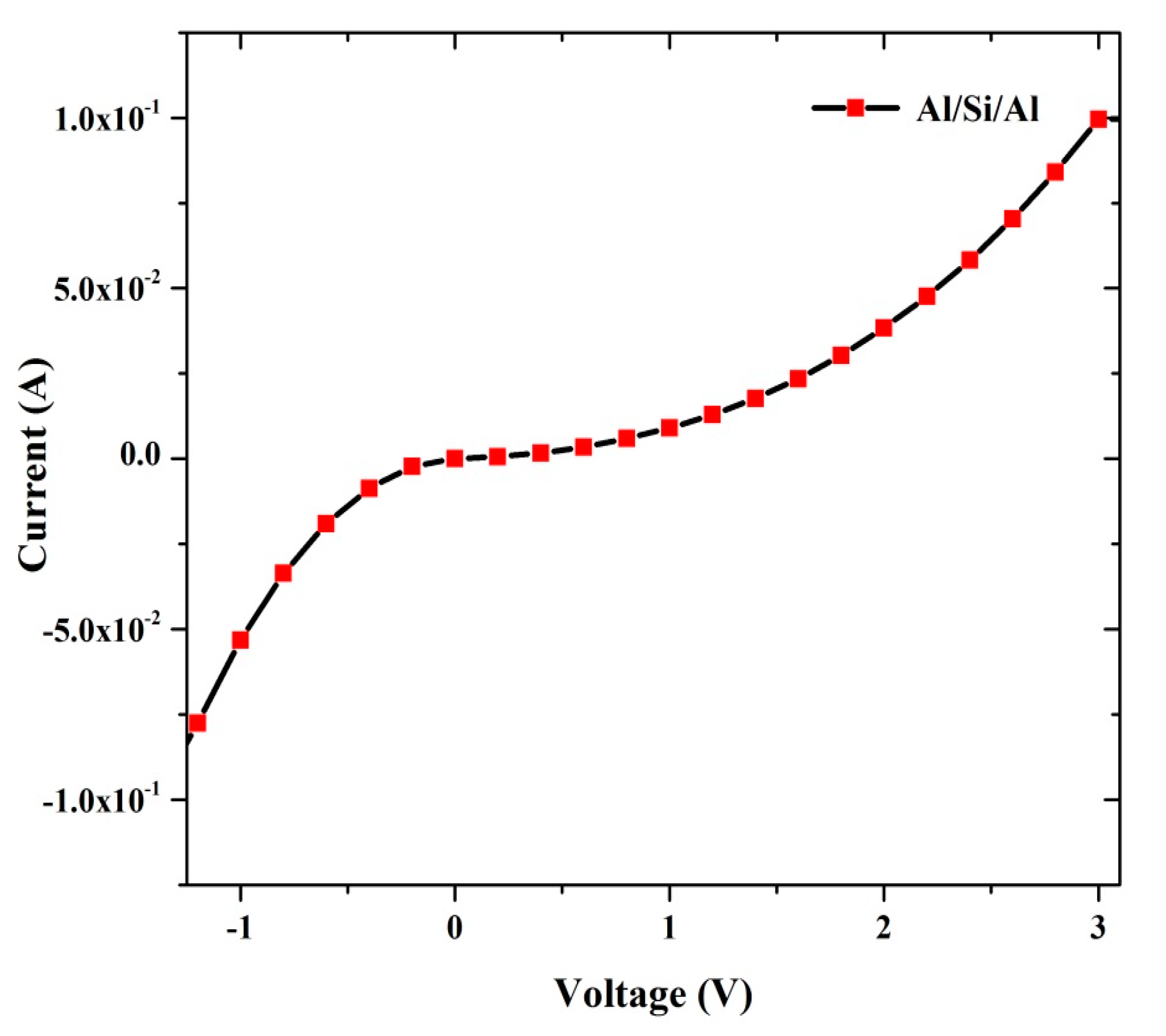
3. Results and Discussions


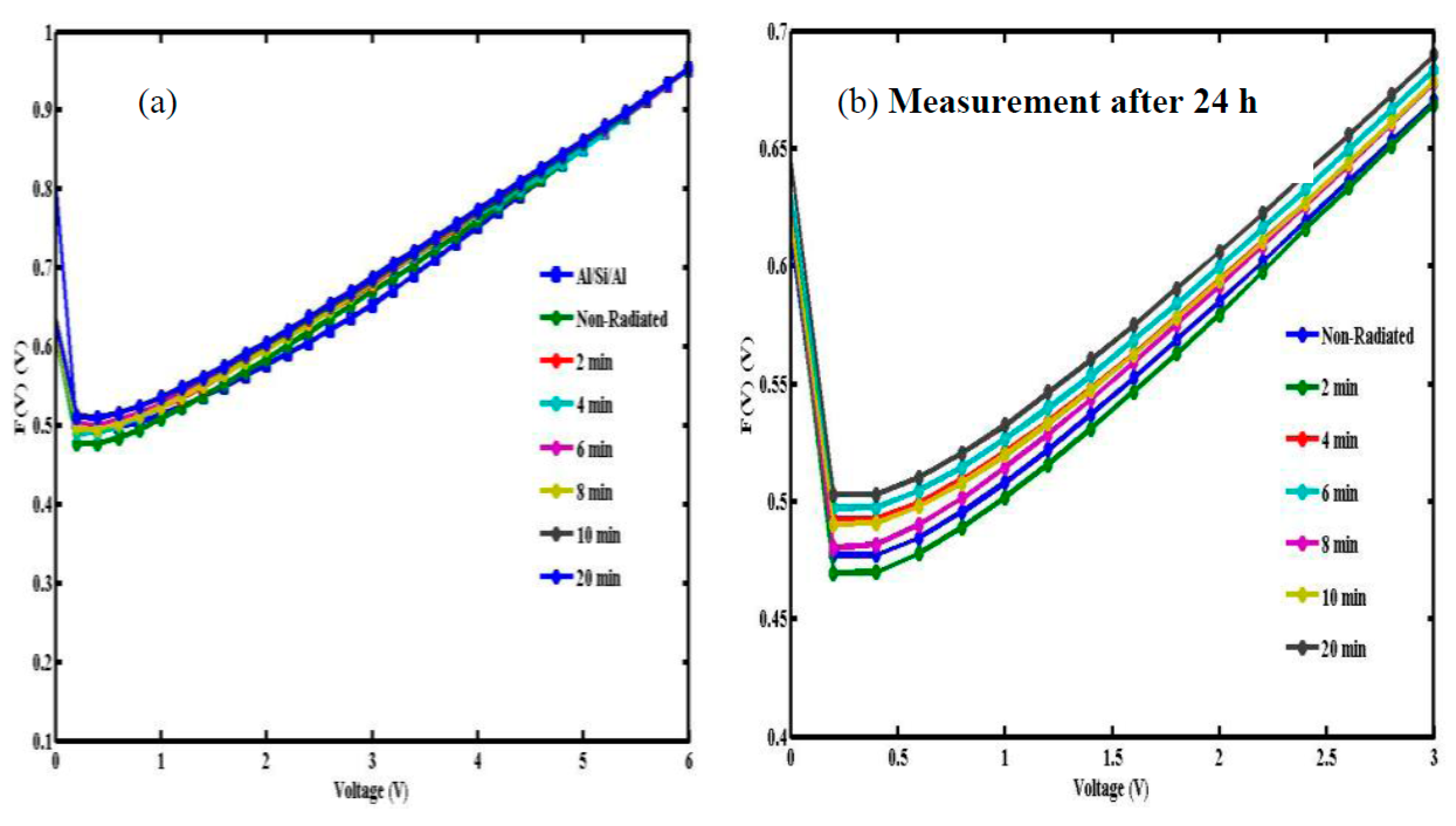
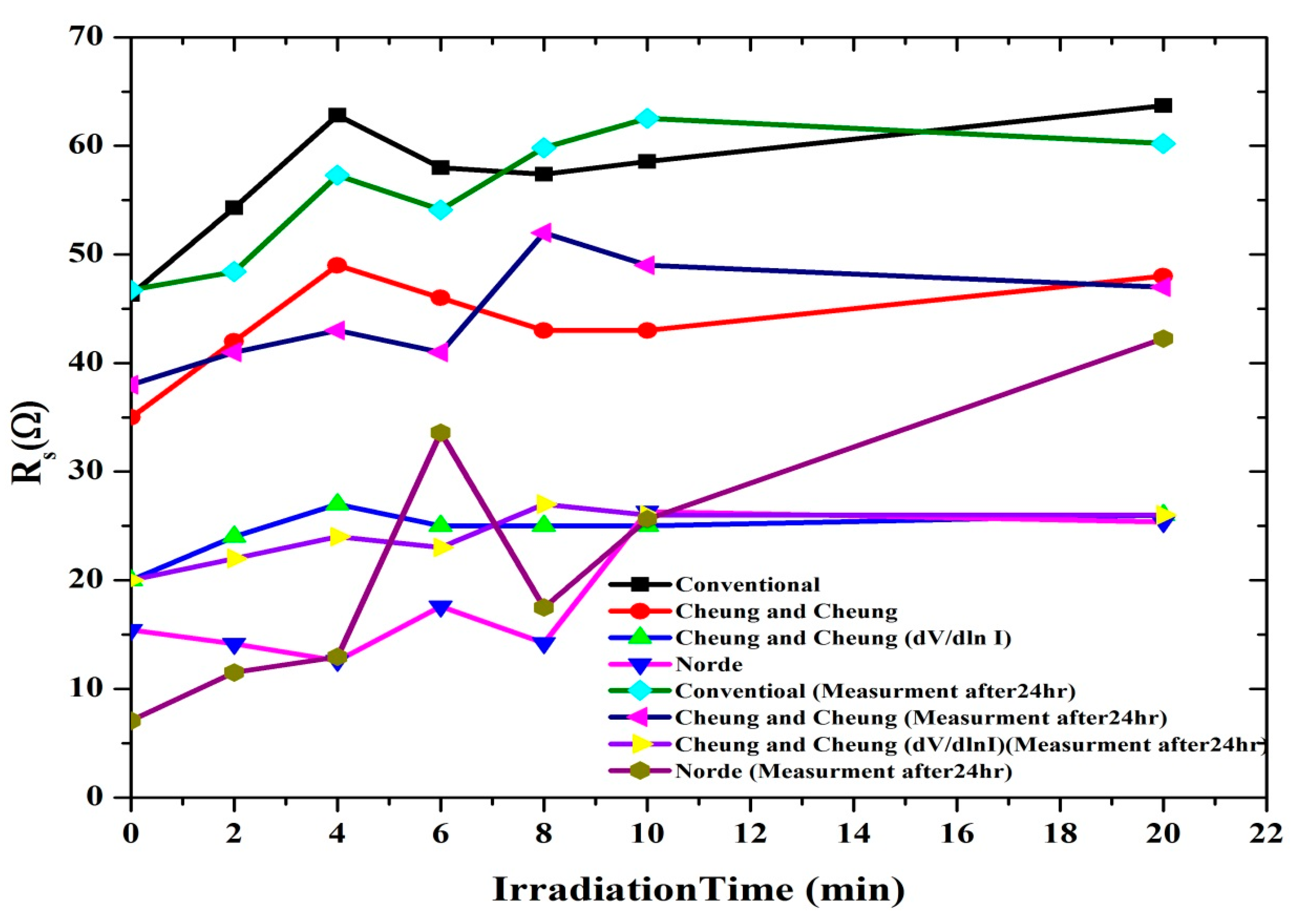
| Radiation Time (min) | Al/DNA/Si/Al and Al/Si/Al | ||||||||||
|---|---|---|---|---|---|---|---|---|---|---|---|
| Conventional Method | Cheung-Cheung Method | Norde Method | |||||||||
| n | Φ (eV) | RS (Ω ) | Φ (eV) | RS (Ω ) | n | RS (Ω ) | F(V)(V) | Φ (eV) | RS (Ω ) | ||
| Al/Si/Al | 7.7478 | 0.5078 | 30.12 | 0.4259 | 41 | 1.5372 | 19.4057 | 0.497 | 0.3634 | 15.3107 | |
| 0 | 9.9719 | 0.4780 | 46.304 | 0.4914 | 35 | 3.0217 | 20 | 0.47729 | 0.3632 | 15.4018 | |
| 2 | 9.7934 | 0.5041 | 54.31 | 0.5208 | 42. | 2.3643 | 24 | 0.495 | 0.3654 | 14.1393 | |
| 4 | 10.5587 | 0.5004 | 62.81 | 0.5304 | 49 | 2.8682 | 27 | 0.4959 | 0.3685 | 12.5607 | |
| 6 | 9.7301 | 0.5026 | 58 | 0.5241 | 46 | 1.5891 | 25 | 0.4984 | 0.3598 | 17.6020 | |
| 8 | 9.7510 | 0.4982 | 57.38 | 0.5538 | 43 | 4.6512 | 25 | 0.5105 | 0.3653 | 14.2170 | |
| 10 | 9.1727 | 0.5190 | 58.56 | 0.5560 | 43 | 3.5271 | 25 | 0.511 | 0.3493 | 26.3337 | |
| 20 | 9.5912 | 0.5063 | 63.69 | 0.5526 | 48 | 4.6512 | 26 | 0.51 | 0.3503 | 25.3676 | |


| Radiation Time (min) | Al/DNA/Si/Al after One Day | ||||||||||
|---|---|---|---|---|---|---|---|---|---|---|---|
| Conventional Method | Cheung-Cheung Method | Norde Method | |||||||||
| n | Φ (eV) | RS (Ω ) | Φ (eV) | RS (Ω ) | n | RS (Ω) | F(V)(V) | Φ (eV) | RS (Ω ) | ||
| 0 | 9.9719 | 0.4780 | 46.72 | 0.4713 | 38 | 3.3721 | 20 | 0.4772 | 0.3834 | 7.0697 | |
| 2 | 10.1446 | 0.4736 | 48.41 | 0.4534 | 41 | 3.3333 | 22 | 0.4697 | 0.3308 | 11.5000 | |
| 4 | 9.9168 | 0.4982 | 57.28 | 0.5042 | 43 | 1.3178 | 24 | 0.4927 | 0.3677 | 12.9375 | |
| 6 | 10.1190 | 0.4982 | 54.11 | 0.5336 | 41 | 3.8760 | 23 | 0.4972 | 0.3030 | 33.5838 | |
| 8 | 10.6707 | 0.4780 | 59.83 | 0.4779 | 52 | 1.3566 | 27 | 0.4805 | 0.3199 | 17.4831 | |
| 10 | 9.7510 | 0.4982 | 62.52 | 0.4923 | 49 | 0.1899 | 26 | 0.4903 | 0.3100 | 25.6188 | |
| 20 | 10.0429 | 0.5078 | 60.22 | 0.5477 | 47 | 5.0388 | 26 | 0.5031 | 0.2971 | 42.2497 | |

| Irradiation Time (min) | Al/DNA/Si/Al | Al/DNA/Si/Al after 24 h | ||
|---|---|---|---|---|
| Region (I) | Region (II) | Region (I) | Region (II) | |
| 0 | 1.16746 | 1.42133 | 1.1481 | 1.4343 |
| 2 | 1.38448 | 1.71641 | 1.22538 | 1.27533 |
| 4 | 1.35663 | 1.84725 | 1.33968 | 1.5977 |
| 6 | 1.38282 | 1.68783 | 1.35636 | 1.74065 |
| 8 | 1.31927 | 1.59468 | 1.18727 | 1.28848 |
| 10 | 1.47493 | 1.82395 | 1.3137 | 1.48376 |
| 20 | 1.3539 | 1.85096 | 1.15171 | 1.77029 |


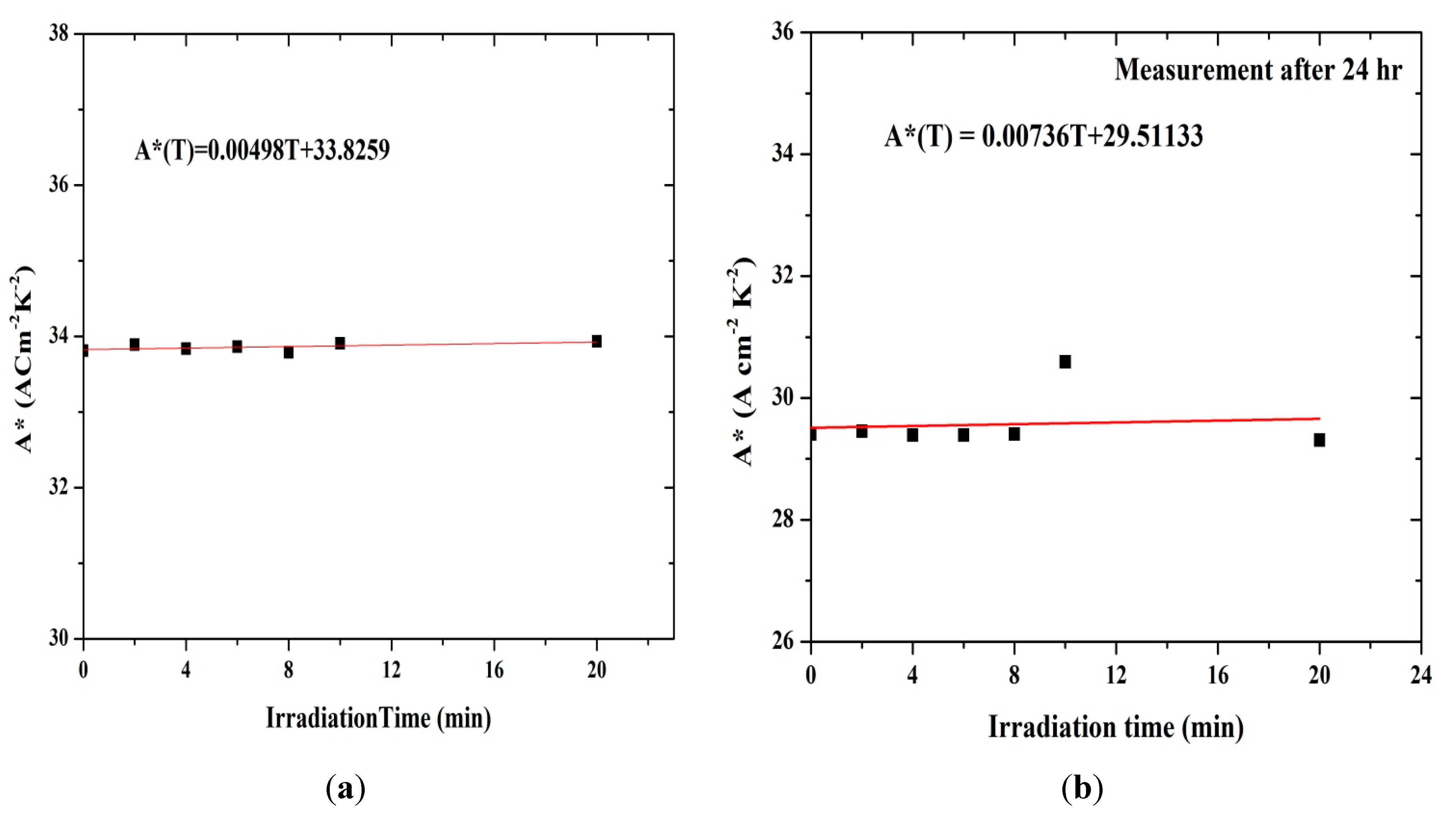
| Irradiation Time (min) | ɸ (eV) | A*(ACm−2K−2) | ɸ (eV) (After 24 h) | A* (ACm−2K−2) (After 24 h) |
|---|---|---|---|---|
| 0 | 0.4816 | 33.80976 | 0.4780 | 29.40648 |
| 2 | 0.5078 | 33.88901 | 0.4736 | 29.45637 |
| 4 | 0.5041 | 33.83585 | 0.4982 | 29.38977 |
| 6 | 0.5063 | 33.86438 | 0.4982 | 29.38978 |
| 8 | 0.5018 | 33.79057 | 0.4780 | 29.40648 |
| 10 | 0.5228 | 33.90649 | 0.4982 | 30.59743 |
| 20 | 0.5101 | 33.93433 | 0.5078 | 29.30825 |
4. Conclusions
Acknowledgments
Author Contributions
Conflicts of Interest
References
- Kažukauskas, V.; Pranaitis, M.; Arlauskas, A.; Krupka, O.; Kajzar, F.; Essaidi, Z.; Sahraoui, B. Electrical and optical properties of thin films of DNA:PEDOT. Opt. Mater. 2010, 32, 1629–1632. [Google Scholar] [CrossRef] [Green Version]
- Aydin, M.E.; Yakuphanoglu, F.; Kılıçoğlu, T. The current-voltage and capacitance–voltage characteristics of molecularly modified β-carotene/n-type Si junction structure with fluorescein sodium salt. Synt. Met. 2007, 157, 1080–1084. [Google Scholar] [CrossRef]
- Al-Ghamdi, A.; Al-Hartomy, O.; Gupta, R.; El-Tantawy, F.; Taskan, E.; Hasar, H.; Yakuphanoglu, F. A DNA Biosensor Based Interface States of a Metal–Insulator–Semiconductor Diode for Biotechnology Applications. Acta Phys. Pol. A 2012, 121, 673–677. [Google Scholar]
- Maas, S.A. Microwave Mixers; Artech House, Inc.: Dedham MA, USA, 1986; Volume 1. [Google Scholar]
- Çaldıran, Z.; Deniz, A.R.; Aydoğan, Ş.; Yesildag, A.; Deniz, D. The barrier height enhancement of the Au/n-Si/Al Schottky barrier diode by electrochemically formed an organic Anthracene layer on n-Si. Superlattices Microstruct. 2013, 56, 45–54. [Google Scholar]
- Kampen, T.; Bekkali, A.; Thurzo, I.; Zahn, D.R.T.; Bolognesi, A.; Ziller, T.; di Carlo, A.; Lugli, P. Barrier heights of organic modified Schottky contacts: Theory and experiment. Appl. Surf. Sci. 2004, 234, 313–320. [Google Scholar] [CrossRef]
- Güllü, Ö.; Türüt, A. Electronic properties of Al/DNA/p-Si MIS diode: Application as temperature sensor. J. Alloys Compd. 2011, 509, 571–577. [Google Scholar] [CrossRef]
- Khatir, N.M.; Banihashemian, S.M.; Periasamy, V.; Ritikos, R.; Majid, W.H. A.; Rahman, S.A. Electrical Characterization of Gold-DNA-Gold Structures in Presence of an External Magnetic Field by Means of I-V Curve Analysis. Sensors 2012, 12, 3578–3586. [Google Scholar] [CrossRef] [PubMed]
- Khatir, N.; Abdul-Malek, Z.; Banihashemian, S. Temperature and Magnetic Field Driven Modifications in the I-V Features of Gold-DNA-Gold Structure. Sensors 2014, 14, 19229–19241. [Google Scholar] [CrossRef] [PubMed]
- Kulkarni, A.; Kim, B.; Dugasani, S.R.; Joshirao, P.; Kim, J.A.; Vyas, C.; Manchanda, V.; Kim, T.; Park, S.H. A novel nanometric DNA thin film as a sensor for alpha radiation. Sci. Rep. 2013, 3, 1–5. [Google Scholar] [CrossRef]
- Bonea, A.; Rau, I.; Tane, A.; Svasta, P. Effects of temperature and humidity on DNA-based biopolymers. J. Optoelectron. Adv. Mater. 2012, 14, 511–516. [Google Scholar]
- Tataroğlu, A.; Altındal, Ş. Gamma-ray irradiation effects on the interface states of MIS structures. Sens. Actuators A Phys. 2009, 151, 168–172. [Google Scholar]
- Güllü, Ö.; Çankaya, M.; Biber, M.; Türüt, A. Gamma irradiation-induced changes at the electrical characteristics of organic-based Schottky structures. J. Phys. D Appl. Phys. 2008, 41. [Google Scholar] [CrossRef]
- Holbert, K.E. Radiation Effects Damage. Available online: http://holbert.Faculty.asu.edu/eee560/Radiation Effects Damage.pdf (accessed on 20 May 2015).
- Ertuğrul, R.; Tataroğlu, A. Effects of gamma irradiation on electrical parameters of metal–insulator–semiconductor structure with silicon nitride interfacial insulator layer. Radiat. Eff. Defects Solids. 2014, 169, 791–799. [Google Scholar] [CrossRef]
- Hibbett, D. Forensic DNA Mini-Prep Using the E.Z.N.A. Kit. Available online: http://www.clarku.edu/faculty/dhibbett/protocols.htm (accessed on 19 May 2015).
- Imtiaj, A.; Lee, T.; Ohga, S. Sequence Variation of Pleurotus Species Collected from Eastern Asia. Micol. Apl. Int. 2011, 23, 1–10. [Google Scholar]
- Cubero, O.F.; Crespo, A.; Fatehi, J.; Bridge, P.D. DNA extraction and PCR amplification method suitable for fresh, herbarium-stored, lichenized, and other fungi. Plant Syst. Evol. 1999, 216, 243–249. [Google Scholar] [CrossRef]
- Tuğluoğlu, N.; Karadeniz, S. Analysis of current–voltage and capacitance–voltage characteristics of perylene-monoimide/n-Si Schottky contacts. Curr. Appl. Phys. 2012, 12, 1529–1535. [Google Scholar] [CrossRef]
- Selçuk, A.B.; Bilge Ocak, S.; Aras, F.G.; Oz Orhan, E. Electrical Characteristics of Al/Poly(methyl methacrylate)/p-Si Schottky Device. J. Electron. Mater. 2014, 43, 3263–3269. [Google Scholar] [CrossRef]
- Gupta, R.K.; Yakuphanoglu, F. Photoconductive Schottky diode based on Al/p-Si/SnS2/Ag for optical sensor applications. Sol. Energy 2012, 86, 1539–1545. [Google Scholar] [CrossRef]
- Reddy, V.R.; Reddy, M.S. P.; Lakshmi, B.P.; Kumar, A.A. Electrical characterization of Au/n-GaN metal–semiconductor and Au/SiO2/n-GaN metal–insulator–semiconductor structures. J. Alloys Compd. 2011, 509, 8001–8007. [Google Scholar] [CrossRef]
- Al-Ta’ii, H.M. J.; Amin, Y.M.; Periasamy, V. Investigations of electrical properties of structures Al-DNA-ITO-Al exposed to alpha particles. Radiat. Meas. 2014, 72, 85–94. [Google Scholar]
- Sawant, S.G.; Zheng, W.; Hopkins, K.M.; Randers-Pehrson, G.; Lieberman, H.B.; Hall, E.J. The Radiation-Induced Bystander Effect for Clonogenic Survival. Radiat. Res. 2002, 157, 361–364. [Google Scholar] [CrossRef] [PubMed]
- Gunduz, B.; Yahia, I.; Yakuphanoglu, F. Electrical and photoconductivity properties of p-Si/P3HT/Al and p-Si/P3HT: MEH-PPV/Al organic devices: Comparison study. Microelectron. Eng. 2012, 98, 41–57. [Google Scholar] [CrossRef]
- Güllü, Ö.; Kilicoglu, T.; Türüt, A. Electronic properties of the metal/organic interlayer/inorganic semiconductor sandwich device. J. Phys. Chem. Solids 2010, 71, 351–356. [Google Scholar] [CrossRef]
- Cheung, S.; Cheung, N. Extraction of Schottky diode parameters from forward current—Voltage characteristics. Appl. Phys. Lett. 1986, 49, 85–87. [Google Scholar] [CrossRef]
- Bazlov, N.V.; Vyvenko, O.F.; Sokolov, P.A.; Kas’yanenko, N.A.; Petrov, Y.V. Charge-controlled fixation of DNA molecules on silicon surface and electro-physical properties of Au–DNA–Si interface. Appl. Surf. Sci. 2013, 267, 224–228. [Google Scholar] [CrossRef]
- Farag, A.A.M.; Gunduz, B.; Yakuphanoglu, F.; Farooq, W.A. Controlling of electrical characteristics of Al/p-Si Schottky diode by tris(8-hydroxyquinolinato) aluminum organic film. Synt. Met. 2010, 160, 2559–2563. [Google Scholar] [CrossRef]
- Karadeniz, S.; Barış, B.; Yüksel, Ö.F.; Tuğluoğlu, N. Analysis of electrical properties of Al/p-Si Schottky contacts with and without rubrene layer. Synt. Met. 2013, 168, 16–22. [Google Scholar]
- Çınar, K.; Coşkun, C.; Aydoğan, Ş.; Asıl, H.; Gür, E. The effect of the electron irradiation on the series resistance of Au/Ni/6H-SiC and Au/Ni/4H-SiC Schottky contacts. Nuclear Instrum. Methods Phys. Res. Sect. B Beam Interact. Mater. Atoms. 2010, 268, 616–621. [Google Scholar]
- Norde, H. A modified forward I-V plot for Schottky diodes with high series resistance. J. Appl. Phys. 2008, 50, 5052–5053. [Google Scholar] [CrossRef]
- Martin, L.M.; Marples, B.; Lynch, T.H.; Hollywood, D.; Marignol, L. Exposure to low dose ionising radiation: Molecular and clinical consequences. Cancer Lett. 2013, 338, 209–218. [Google Scholar] [CrossRef] [PubMed]
- Hsiung, C.-M.; Chou, C.-S.; Chiang, T.-L. A generalized Norde plot for reverse biased Schottky contacts. Int. J. Miner. Metall. Mater. 2012, 19, 54–58. [Google Scholar] [CrossRef]
- Al-Ta’ii, H.; Amin, Y.; Periasamy, V. Calculation of the Electronic Parameters of an Al/DNA/p-Si Schottky Barrier Diode Influenced by Alpha Radiation. Sensors 2015, 15, 4810–4822. [Google Scholar] [CrossRef] [PubMed]
- Güllü, Ö.; Çankaya, M.; Barış, Ö.; Türüt, A. DNA-based organic-on-inorganic devices: Barrier enhancement and temperature issues. Microelectron. Eng. 2008, 85, 2250–2255. [Google Scholar]
- Avdoğan, Ş.; Türüt, A. Influence of 12 MeV electron irradiation on the electrical and photovoltaic properties of Schottky type solar cell based on Carmine. Radiat. Phys. Chem. 2011, 80, 869–875. [Google Scholar] [CrossRef]
- Güllü, Ö.; Avdoğan, Ş.; Şerifoğlu, K.; Türüt, A. Electron irradiation effects on the organic-on-inorganic silicon Schottky structure. Nucl. Instrum. Meth. A 2008, 593, 544–549. [Google Scholar] [CrossRef]
- Umana-Membreno, G.; Dell, J.; Parish, G.; Nener, B.; Faraone, L.; Mishra, U. 60 Co gamma irradiation effects on n-GaN Schottky diodes. IEEE Trans. Electron. Devices 2003, 50, 2326–2334. [Google Scholar] [CrossRef]
- Tung, R. Electron transport at metal-semiconductor interfaces: General theory. Phys. Rev. B 1992, 45, 13509. [Google Scholar] [CrossRef]
- Hassan, M.A.-T. Hypersensitivity phenomenon in hydatid protoscolices irradiated by alpha particles. J. Kerbala Univ. 2012, 10, 41–44. [Google Scholar]
- Faika, A.; Azooz, H.M.A.-T.; Ahmad, K.D. Observation of Hypersensitivity Phenomena in E-Coli Cells after Irradiation by Alpha Particles. J. Rafiden Sci. 2009, 20, 113–120. [Google Scholar]
- Mtangi, W.; Auret, F.D.; Nyamhere, C.; Janse van Rensburg, P.J.; Chawanda, A. Analysis of temperature dependent measurements on Pd/ZnO Schottky barrier diodes and the determination of the Richardson constant. J. Phys. Condens. Matter 2009, 404, 1092–1096. [Google Scholar]
© 2015 by the authors; licensee MDPI, Basel, Switzerland. This article is an open access article distributed under the terms and conditions of the Creative Commons Attribution license (http://creativecommons.org/licenses/by/4.0/).
Share and Cite
Al-Ta'ii, H.M.J.; Periasamy, V.; Amin, Y.M. Electronic Properties of DNA-Based Schottky Barrier Diodes in Response to Alpha Particles. Sensors 2015, 15, 11836-11853. https://doi.org/10.3390/s150511836
Al-Ta'ii HMJ, Periasamy V, Amin YM. Electronic Properties of DNA-Based Schottky Barrier Diodes in Response to Alpha Particles. Sensors. 2015; 15(5):11836-11853. https://doi.org/10.3390/s150511836
Chicago/Turabian StyleAl-Ta'ii, Hassan Maktuff Jaber, Vengadesh Periasamy, and Yusoff Mohd Amin. 2015. "Electronic Properties of DNA-Based Schottky Barrier Diodes in Response to Alpha Particles" Sensors 15, no. 5: 11836-11853. https://doi.org/10.3390/s150511836
APA StyleAl-Ta'ii, H. M. J., Periasamy, V., & Amin, Y. M. (2015). Electronic Properties of DNA-Based Schottky Barrier Diodes in Response to Alpha Particles. Sensors, 15(5), 11836-11853. https://doi.org/10.3390/s150511836