
Article

Cu-Substituted Sb2S3 Nanopowders—Structural, Microstructural and Optical Analyses

by
Nikola Ilić
1,*,
Cristian Radu
2,
Amelia Elena Bocirnea
2,
Aurelian Catalin Galca
2 and
Ivana Validžić
1
1
Department of Atomic Physics, Vinča Institute of Nuclear Sciences, National Institute of the Republic of Serbia, University of Belgrade, 11000 Belgrade, Serbia
2
National Institute of Materials Physics, Atomistilor 405A, 077125 Magurele, Romania
*
Author to whom correspondence should be addressed.
Int. J. Mol. Sci. 2026, 27(16), 7406; https://doi.org/10.3390/ijms27167406
Submission received: 12 July 2026 / Revised: 13 August 2026 / Accepted: 14 August 2026 / Published: 19 August 2026

Abstract

Cu(I)-doped Sb2S3 powders were synthesized using the hot-injection method, with the aim of reducing crystalline particle size and tailoring their morphology to make them more spherical and better suited for spray deposition as an absorber layer in photovoltaic devices. Structural and microstructural analyses confirmed the successful formation of elongated (rod-like) crystalline Sb2S3 particles. CuSbS2, itself a semiconducting material with a high light-absorption coefficient, formed in large amounts in Cu-doped systems, in the form of agglomerates of platelet-like particles. The third abundant phase was an amorphous phase present as spherical nanoparticles composed of uniformly distributed Sb, Cu and S. The presence of Cu decreased Sb2S3 particle size but did not significantly influence its morphology. Chlorides in the synthesis solution enabled faster crystallization than when acetates are the only present anionic species. When Cu, Sb and S sources were added during hot injection in stoichiometric amounts to form CuSbS2, this phase was not reached, and Cu9S5 and Cu12Sb4S13 were the dominant phases, indicating Cu-rich phases have a higher tendency to crystallize in specific conditions with an excess of antimony, and, potentially, sulfur is needed to obtain pure CuSbS2.

1. Introduction

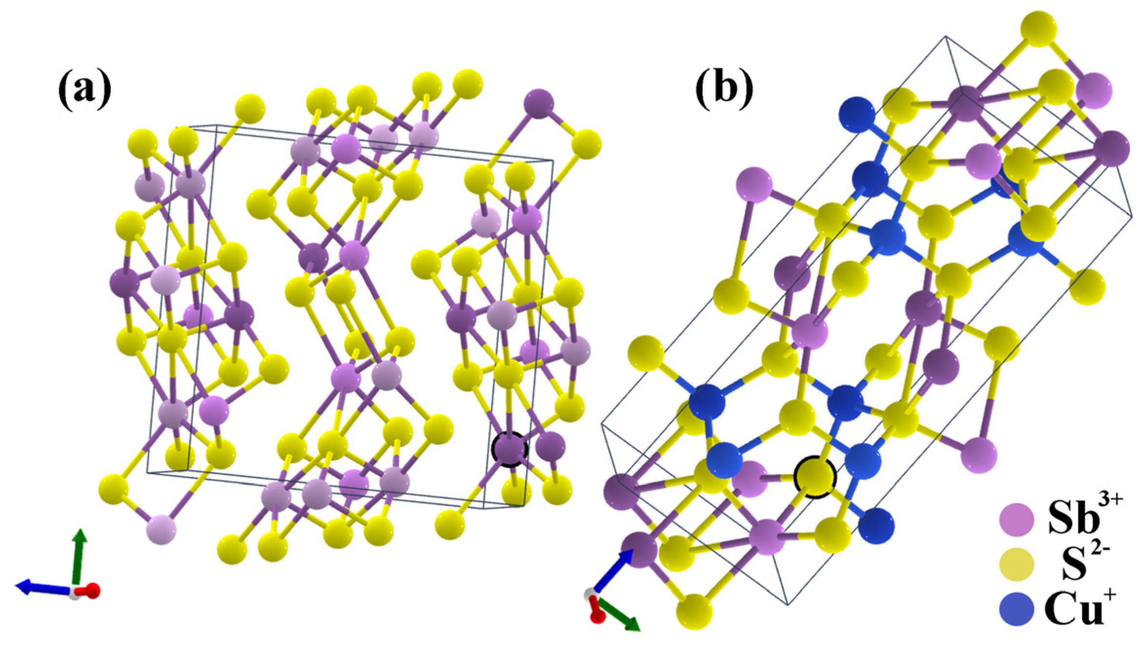
Antimony sulfide, Sb2S3, is currently an interesting subject of research in the field of photovoltaics owing to its abundant components and suitable optical properties: band gap in the visible-light range (1.5–2.2 eV), high light-absorption coefficient in the range of 104–105 cm−1 and a high refractive index (2.5–2.8). For this reason, light-absorber layers based on Sb2S3 have been recently studied often in photovoltaic devices, especially under low-light conditions [1,2]. Sb2S3 crystallizes as an orthorhombic structure, with two different Sb positions (coordination numbers 3 and 5) and two S positions (coordination numbers 2 and 3) covalently bonding to create quasi 1D [Sb4S6]n ribbons interconnected with van der Waals bonds, as schematically represented in Scheme 1a. This structure creates non-isometric electrical and optical properties, which complicate high photoconversion efficiency and application in photovoltaics [3]. Crystalline Sb2S3 is usually reported to be a direct band gap material with a band gap in the lower range (1.5–1.7 eV), appropriate to be excited by visible light. Amorphous Sb2S3 has a larger band gap (1.7–2.2 eV), utilizing the narrower spectral range, and has a lower absorption level due to being indirect [4].
The hot-injection synthesis route developed by our group [5,6] enables completely homogeneous mixing with doping ions at any ratio. It also allows fast and uniform nucleation and growth of crystals. Previous studies showed that antimony substitution with copper influences the growth of crystals during synthesis, enhances light absorption and lowers the band gap, so this study was conducted to better understand how copper ions modify the structure, microstructure and optical properties of Sb2S3 [7,8,9,10].
There is another consequence of the specific structure of Sb2S3. Structural 1D orientation leads to the formation of 1D microstructures upon the crystallization of particles [3]. It is challenging to deposit these particles uniformly without their spontaneous orientation and agglomeration. Therefore, it is beneficial to identify a method to prevent the one-dimensional growth of particles and to make them as close to spherical as possible before their deposition as a component of a solar cell.
Chalcostibite, CuSbS2, is another promising light-absorber material for photovoltaics. It exhibits similar properties to Sb2S3, including a suitable bandgap (1.4–1.6 eV), large optical absorption coefficient (105 cm−1), good stability, nontoxicity and abundant constituents. It crystallizes in an orthorhombic 2D-layered structure (Pnma space group) of Cu-S pentahedra and Sb-S tetrahedra with a unit cell composed of four formula units, as schematically represented in Scheme 1b. Other copper antimony sulfide systems like skinnerite (Cu3SbS4), fematinite (Cu3SbS4) and tetrahedrite (C12Sb4S13) exhibit similar optical properties and are worth studying in the field of photovoltaics [11,12,13,14,15,16,17,18,19,20].
Sb2S3 has an orthorhombic Pnma structure, and it is complicated to predict the radii or preferable position of substituting ions. The nature of bonds is more covalent, and two different coordination numbers (CN) of Sb(III) ions (CN3—dominantly covalent, and CN5—three covalent and two van der Waals bonds) give a complex 1D structure with an unknown radius of Sb [21,22]. Cu(I) typically does not crystallize in this coordination, but if we compare the ionic radii of the two hexacoordinated ions, they are very similar: Sb(III) (0.76 Å) and Cu(I) (0.77 Å); so, a successful substitution may potentially happen [23]. The electronegativities of Cu and Sb are similar, measuring 1.9 and 2.05 on the Pauling scale, so, on that side, they compose a suitable substitution pair (https://pubchem.ncbi.nlm.nih.gov/ptable/electronegativity/ (accessed on 1 July 2026)).

2. Results and Discussion

2.1. XRD Analysis

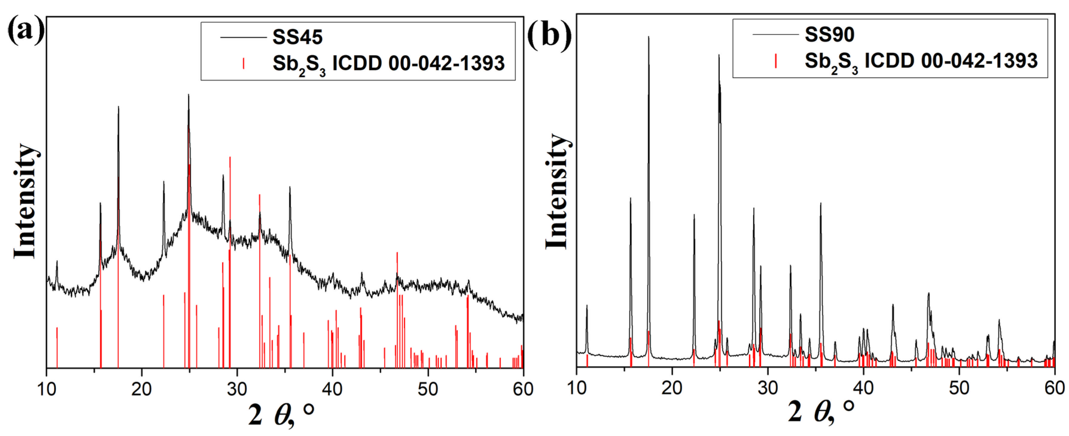
The development of the structure during hot injection in the initial period is presented in Figure 1 at the angles of the most prominent peaks. Orthorhombic Sb2S3 is the first phase that crystallizes from the amorphous phase, and it is already evident after 45 s, with better development and growth of crystals after 90 s.
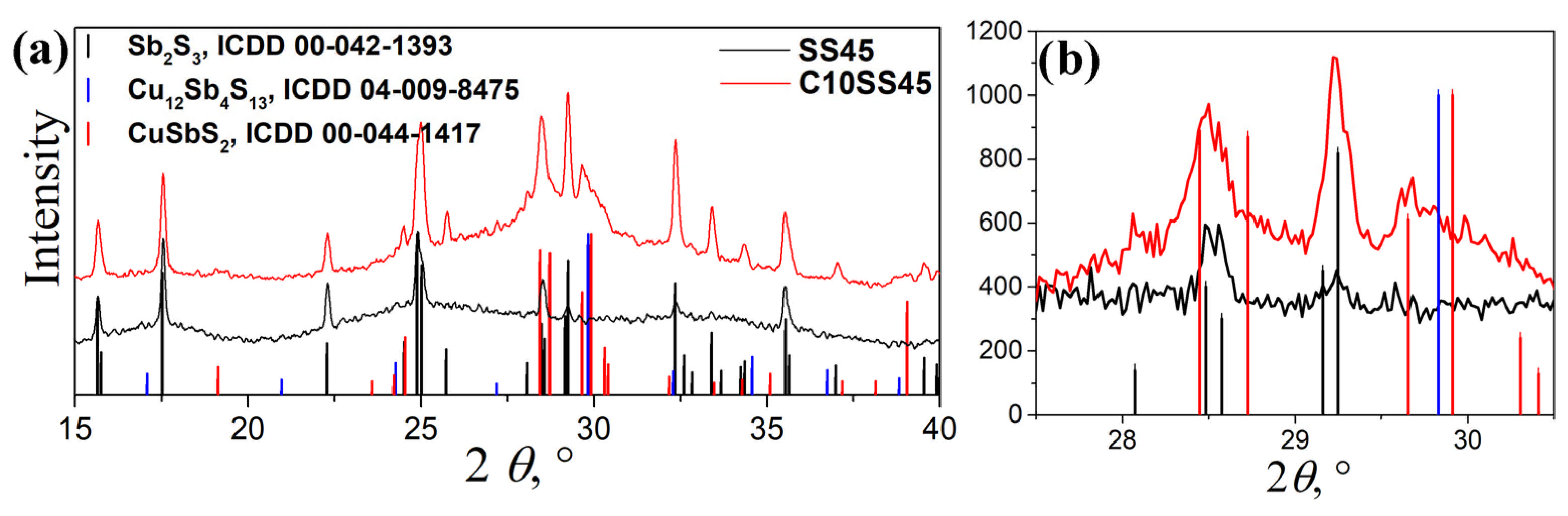
In the presence of Cu substituting 10% of Sb, the crystallinity mildly improves after 45 s of synthesis, as can be seen in Figure 2a. A slight orientation change is visible in the enlarged spectra at 2θ = 27.5–30.5° in Figure 2b. Copper-containing phases were not detected.
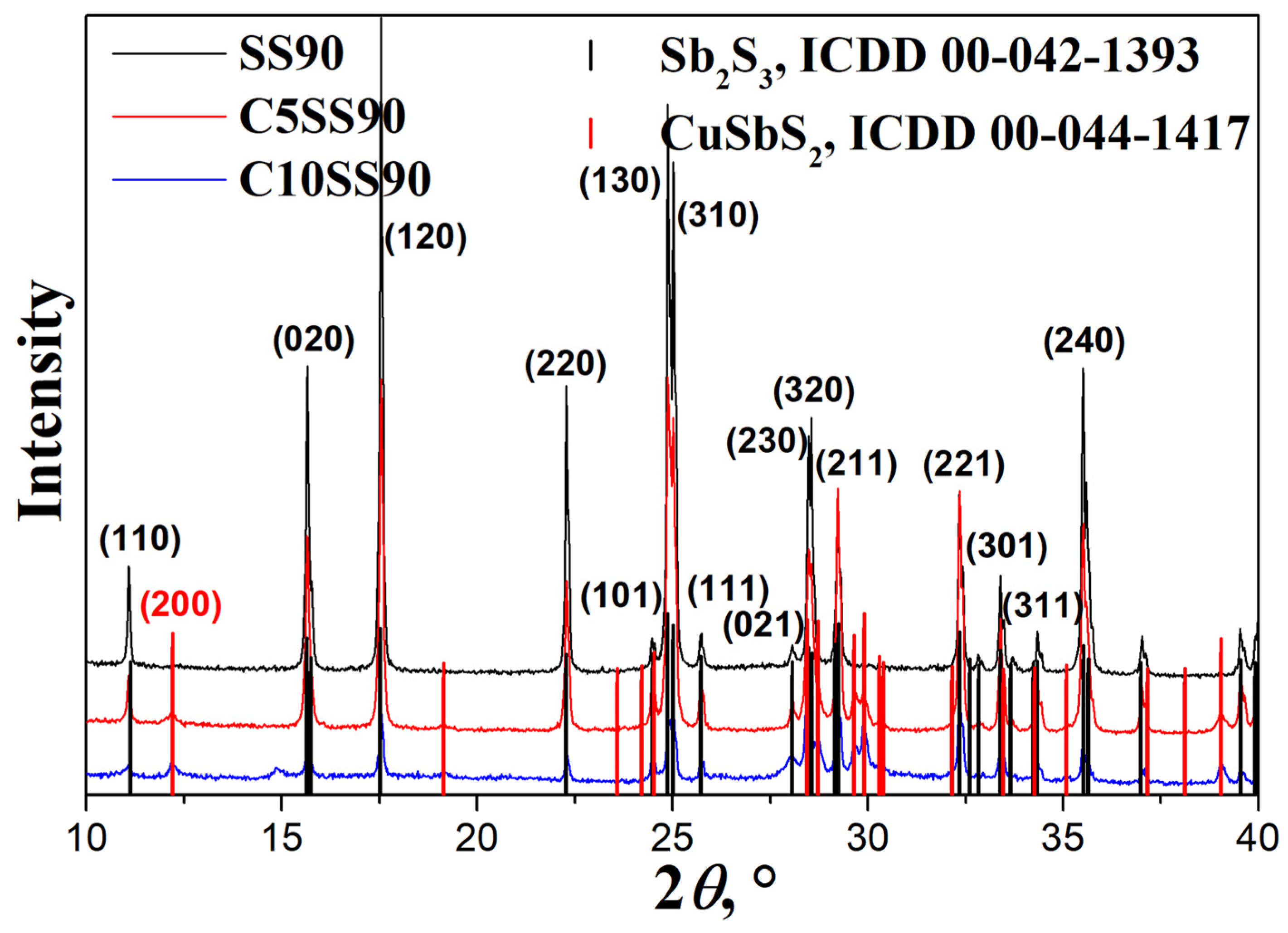
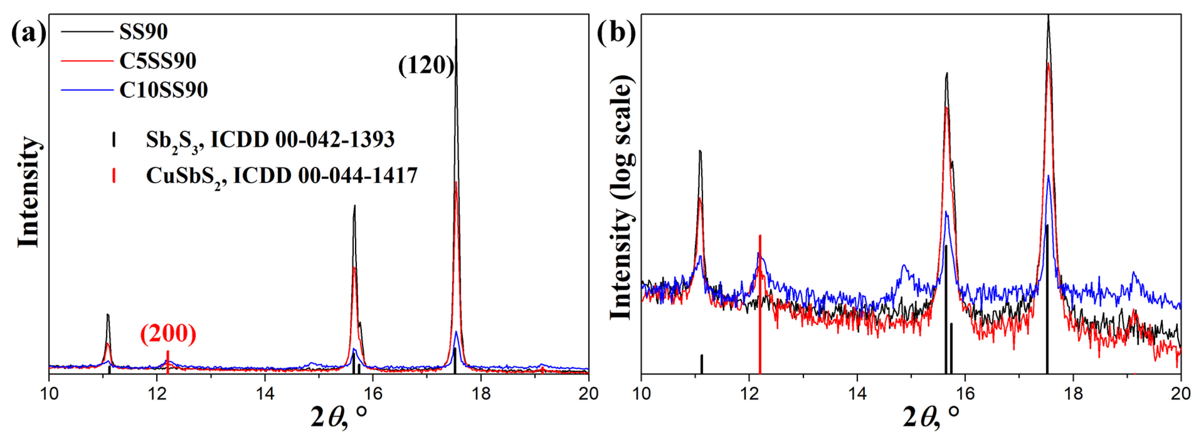
After doubling the reaction time to 90 s, Cu-substituted Sb2S3 samples show lower crystallinity than pristine ones, as can be seen in Figure 3, with a clearly modified orientation, and the most intense peaks for C10SS90 are (211) and (221). In SS90, (120), (130), (230), (220) and (240) planes had the maximal intensity, as well as for C5SS90, though a decrease in these peaks and increase in (211) and (221) can be observed for the 5% Cu substitution level. The position of the peaks is unchanged, implying the copper ions may not actually be incorporated into the structure of Sb2S3, but rather some other phase. The impact of Cu substitution on the structure is more obvious at the enlarged section of 2θ between 10 and 20°, presented in Figure 4a. The highlighted low-intensity peak of the CuSbS2 phase is obvious if the intensity in this region is presented with a logarithmic scale (Figure 4b). A significant secondary CuSbS2 phase formed at both the 5% and 10% substitution levels, which is often reported for Cu-substituted Sb2S3 [24]. The content of phases, calculated based on the (120) peak of Sb2S3 and (200) peak of CuSbS2, shows a CuSbS2 phase composed 6.6% wt of C5SS sample and 27.0% wt of C10SS sample, which corresponds to 5.0% and 16.7% of Cu incorporation into the product, in the form of the CuSbS2 phase. All the other secondary phases remained under the limit of detection. The reaction yield is not 100% and that may be the reason for more Cu in the product than in the added reactants.
The chemistry of synthesis solutions strongly influences the kinetics of processes. When Sb(III) acetate was used as a source of Sb instead of SbCl3, the powders remained completely amorphous after 90 s, and a longer reaction time was needed to achieve crystallization (Figure S1 in the Supplementary Materials). The presence of copper did not significantly influence crystallinity, similarly to the synthesis with chlorides present. Chlorides in the system promote precipitation.

2.2. Raman Analysis

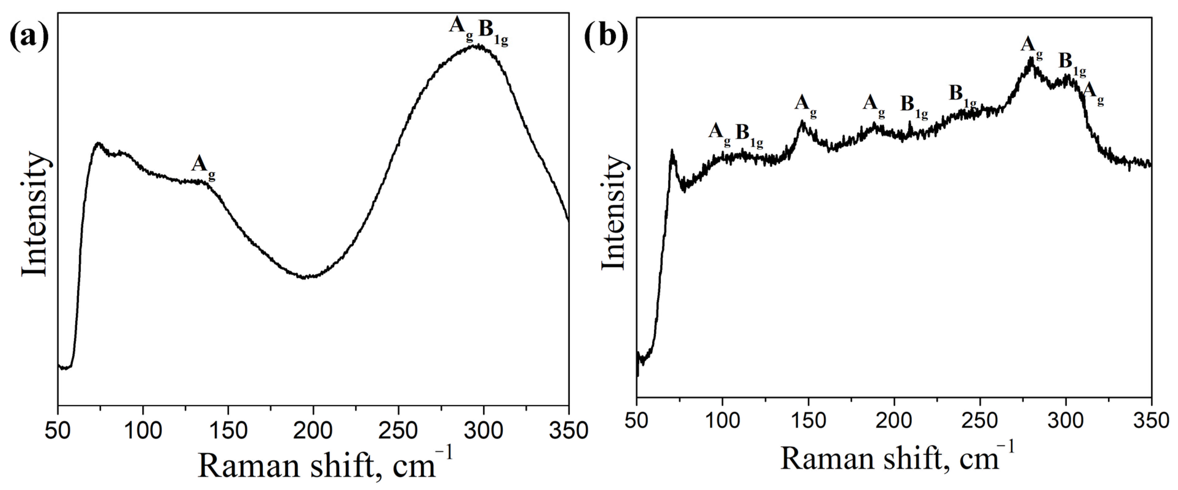
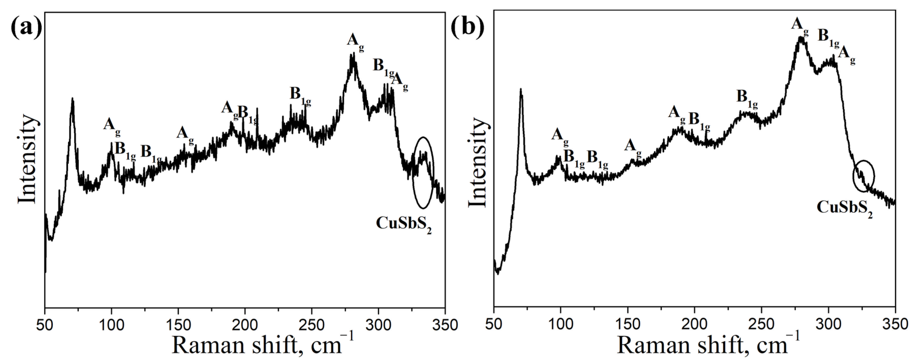
The amorphous SS45 powder (Figure 5a) shows the characteristic most-intense Ag modes of Sb-S bonds, which are starting to form [25,26]. Crystalline SS90 samples exhibit bright rod-like particles and gray powdery areas under optical microscope (Figure S2a,b), but those two regions show very similar Raman responses (Figure S2d) with nine of the typical 10 Ag and B1g modes of Sb2S3 crystalline phase observed, confirming the similar structure between the two morphologies [27]. Bigger white particles observed in small number in powders (Figure S2c) were identified by the Raman analysis of spectra presented in Figure S2e as the bulk antimony phase (bands at 109 and 146 cm−1), though antimony is present in some other regions independently of the observed microstructures. Peaks related to the Sb2O3 oxide phase may become evident at 188 and 251 cm−1, like it may be seen in Figure S2e, but the oxide phase is not inherently present in powders. When using the lower power of the laser (neutral density filter ND5 instead of ND3 or ND1) in the Raman analysis (like in Figure 5b), the oxides are absent, so their occurrence is related to thermal oxidation under the laser beam in an air atmosphere [26,27].
Cu-doped samples (Figure 6) did not exhibit many differences in their Raman responses except for the noticeable presence of a band at around 330 cm−1, corresponding to the CuSbS2 phase in Cu-substituted samples, also detected by XRD analysis [13].

2.3. TEM Analysis

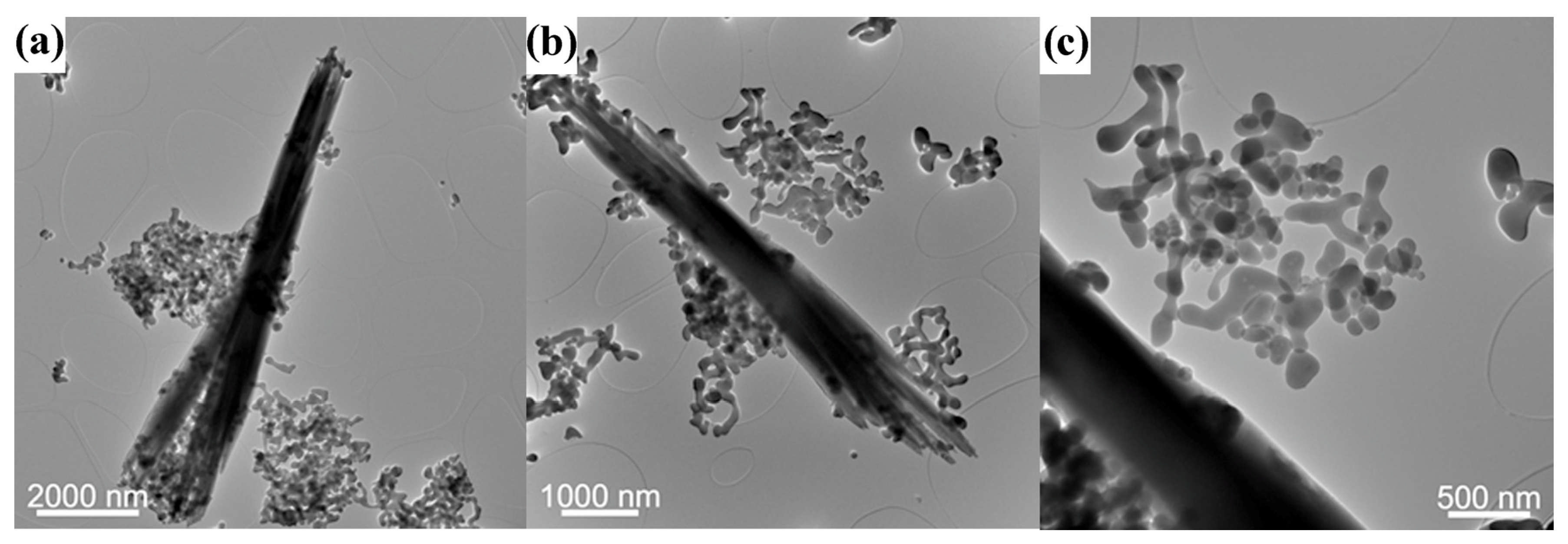
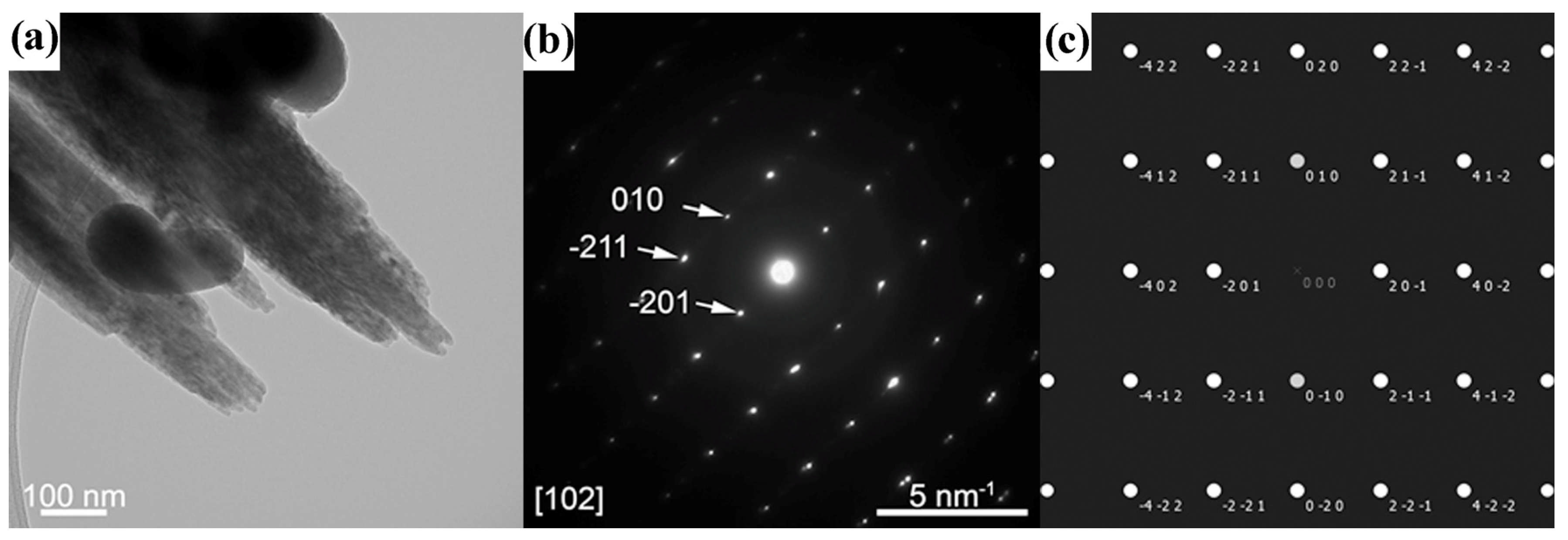
Sample SS45 exhibited several-microns-long needle-like particles bundled together, as well as smaller particles with irregular shapes, ranging from spherical particles with a ~100 nm diameter to elongated structures made of several connected spherical particles, as seen in Figure 7. The selected area electron diffraction (SAED) pattern of the crystalline microrods observed in Figure 8a confirms that the crystalline phase is Sb2S3 as seen in Figure 8b. The spots that correspond to the lattice planes (010)—3.83 Å, (−211)—3.05 Å and (−201)—5.05 Å are marked. The zone axis [102] is perpendicular to these planes, giving the crystal orientation. The same results were obtained by measuring the interplanar distances in the spherical particle in the HRTEM image using Fourier transform (FFT) in Figure S3 (Supplementary Materials). Both the SAED pattern and the FFT are comparable with a simulated diffraction pattern image, as seen in Figure 8c, confirming the Sb2S3 phase.
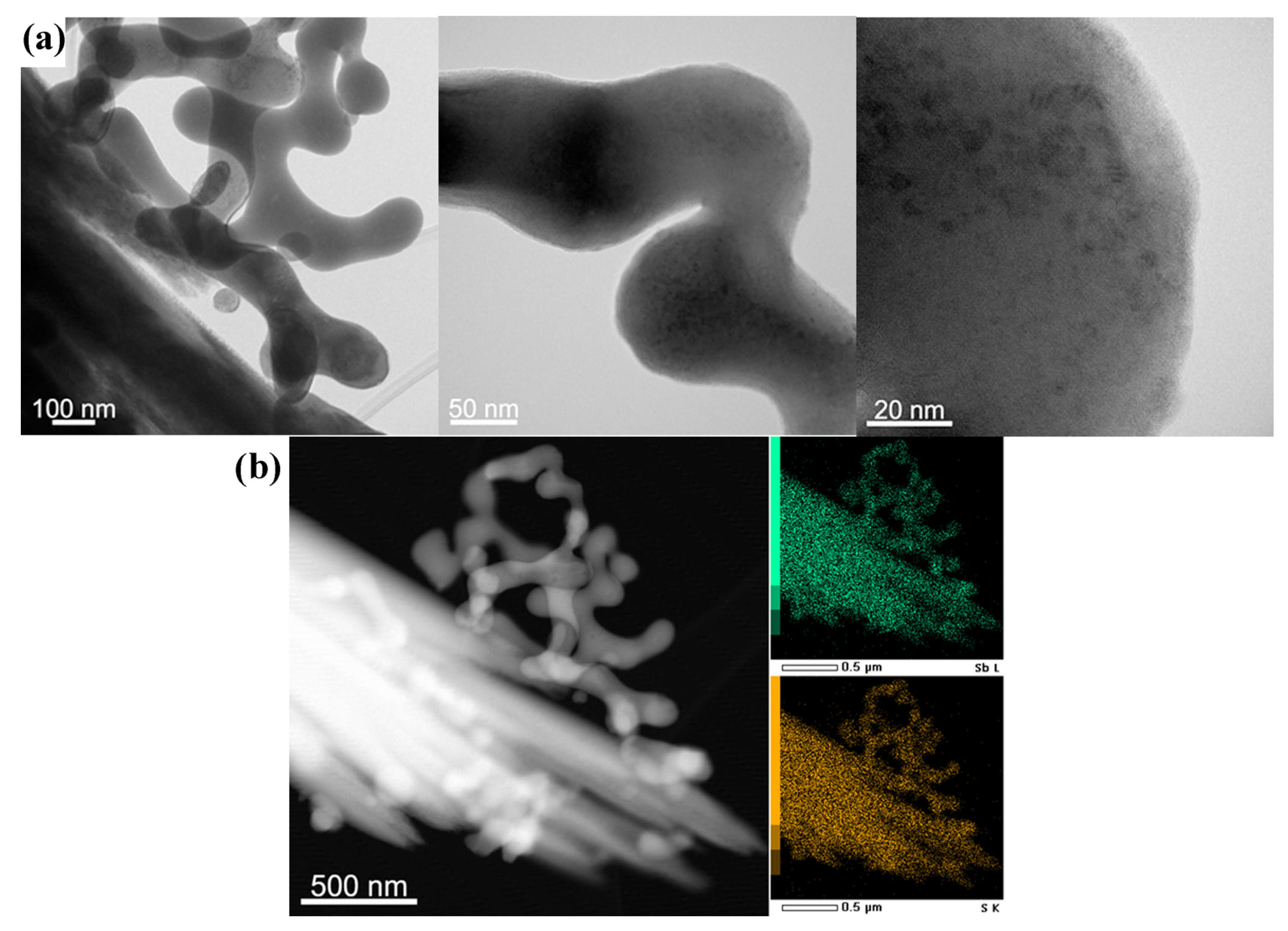
The images in Figure 9a reveal that the spherical conjoined nanoparticles differ structurally. They are mostly amorphous, but a crystalline phase is also observed in them. The crystalline phase was confirmed to be Sb2S3. The mapping (Figure 9b) and EDS spectra (Figure S4) show uniform distributions of Sb and S in all particles. HRTEM images revealed that these nanoparticles in SS45 may be both amorphous and crystalline, showing that the characteristic process of the 1D rod-like particle formation of Sb2S3 takes place 45 s into the reaction. According to XRD, this sample is predominantly amorphous with initial crystallization observed by the separation of the sharp low-intensity Sb2S3 peak (Figure 1 and Figure 2), meaning the amorphous nanoparticle aggregates are the dominant morphology.
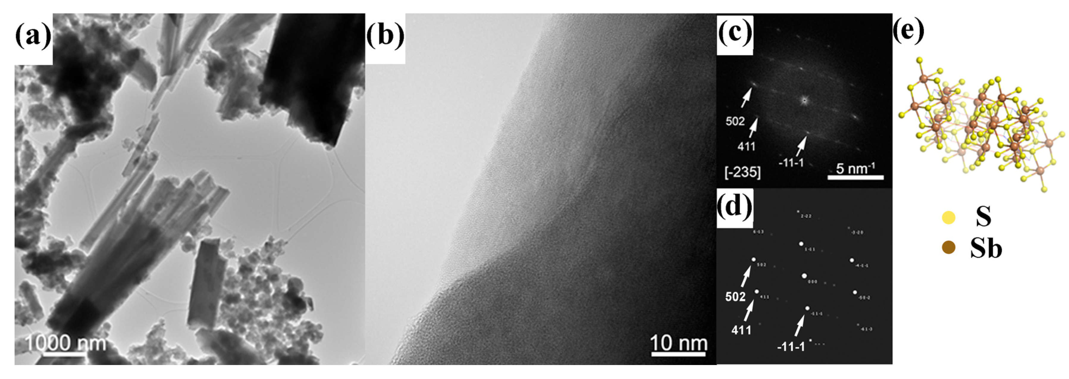
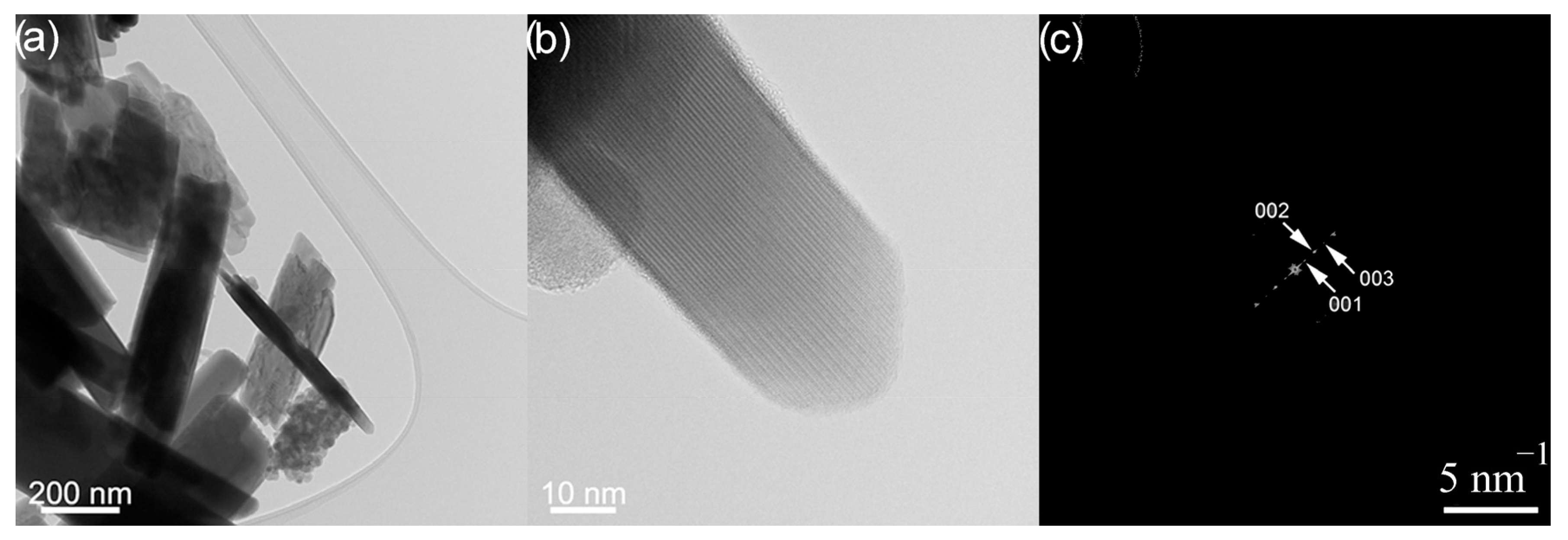
The TEM investigation of sample SS90 reveals a similar presence of two distinct morphologies (Figure 10). Elongated crystalline rod-like particles are present to greater extent, alongside a significant amount of particles with different shapes. The elongated particles are of similar sizes to those in SS45 powders with a length above 1000 nm (reaching up to 5000 nm) and width between 200 and 300 nm (reaching over 1000 nm), with an aspect ratio of 5:1. The HRTEM image in Figure 10b was analyzed by taking the Fourier transform of the area in which lattice fringes were visible. The obtained FFT pattern (Figure 10c) displays bright spots compatible with the (502), (411) and (−11−1) interplanar distances of Sb2S3. The simulated diffraction pattern and structural model of the Sb2S3 crystal are displayed in Figure 10d,e.
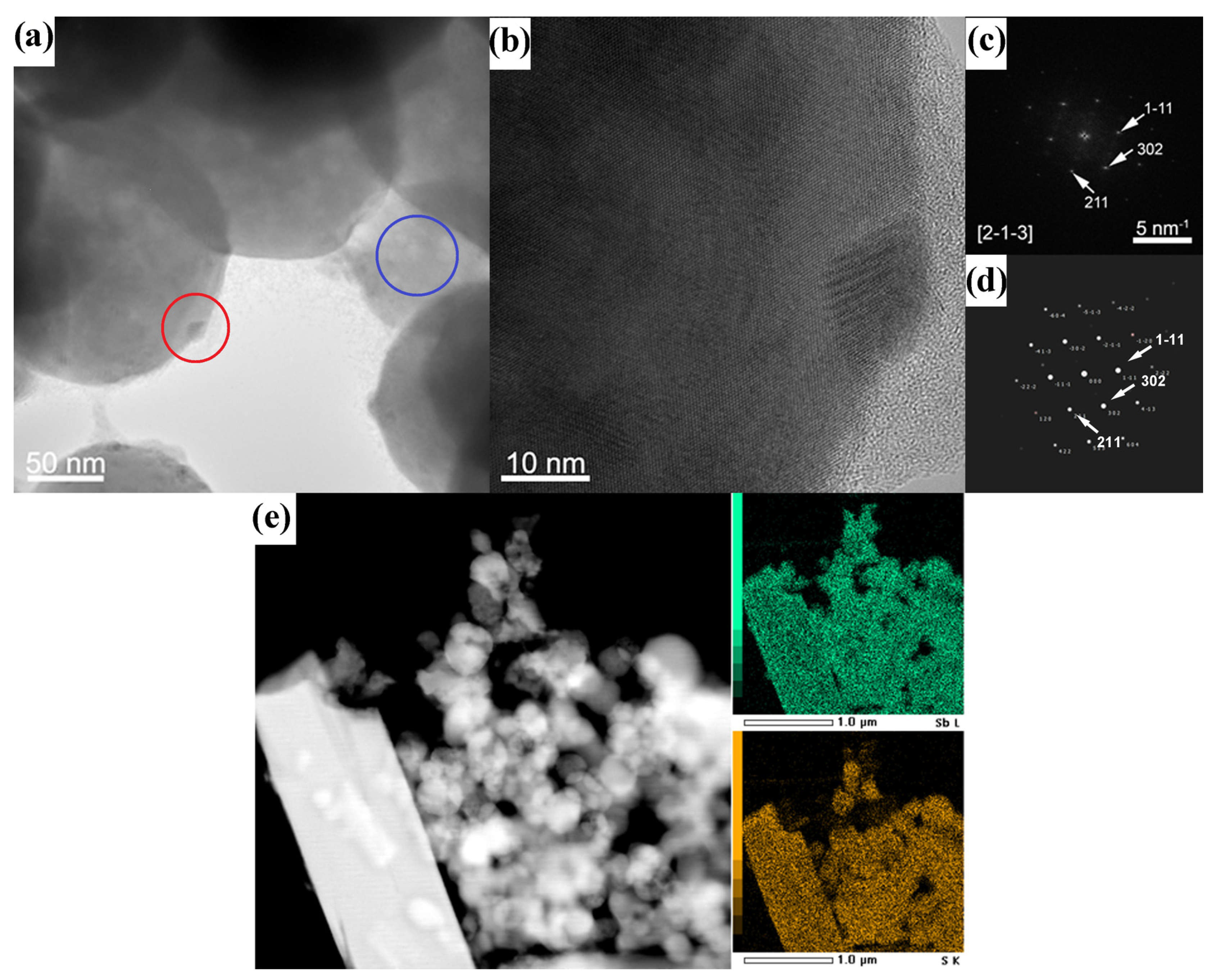
The spherical nanoparticles presented in TEMs in Figure 11a are mostly above 100 nm in diameter and appear amorphous, but small nanocrystalline domains may be observed on their surfaces—like the red circled area in Figure 11a. Some particles display porous-like features, as those seen in the blue circle in Figure 11b. The FFT analysis performed on such spherical nanoparticles, presented in Figure 11c, indicates that the lattice fringes visible in the HRTEM image correspond to those of a Sb2S3 crystal oriented along the [2−1−3] zone axis. The comparison with the simulated electron diffraction pattern (Figure 11d) confirms that the phase is Sb2S3. The phase of the nanoparticles present on the surface of the large spherical particles was not identified.
The STEM-EDX analysis performed on the area in Figure 11e shows that there are some areas with amorphous particles in which the S signal is not present, which may explain the Sb-rich areas observed under Raman analysis (Figure 5b). The rest of the map displays homogeneous distributions of S and Sb in both spherical and elongated nanoparticles, reaffirming that the two types of particles belong to the same phase but appear in different morphologies. No differences in the concentration were observed. Small spots can be seen in some spherical particles with a different level of contrast to the surrounding material, resembling porous areas in Figure 11a, which is usually associated with the smaller average atomic number of the material in that area or indicates that there is a pore in the crystal structure [28].
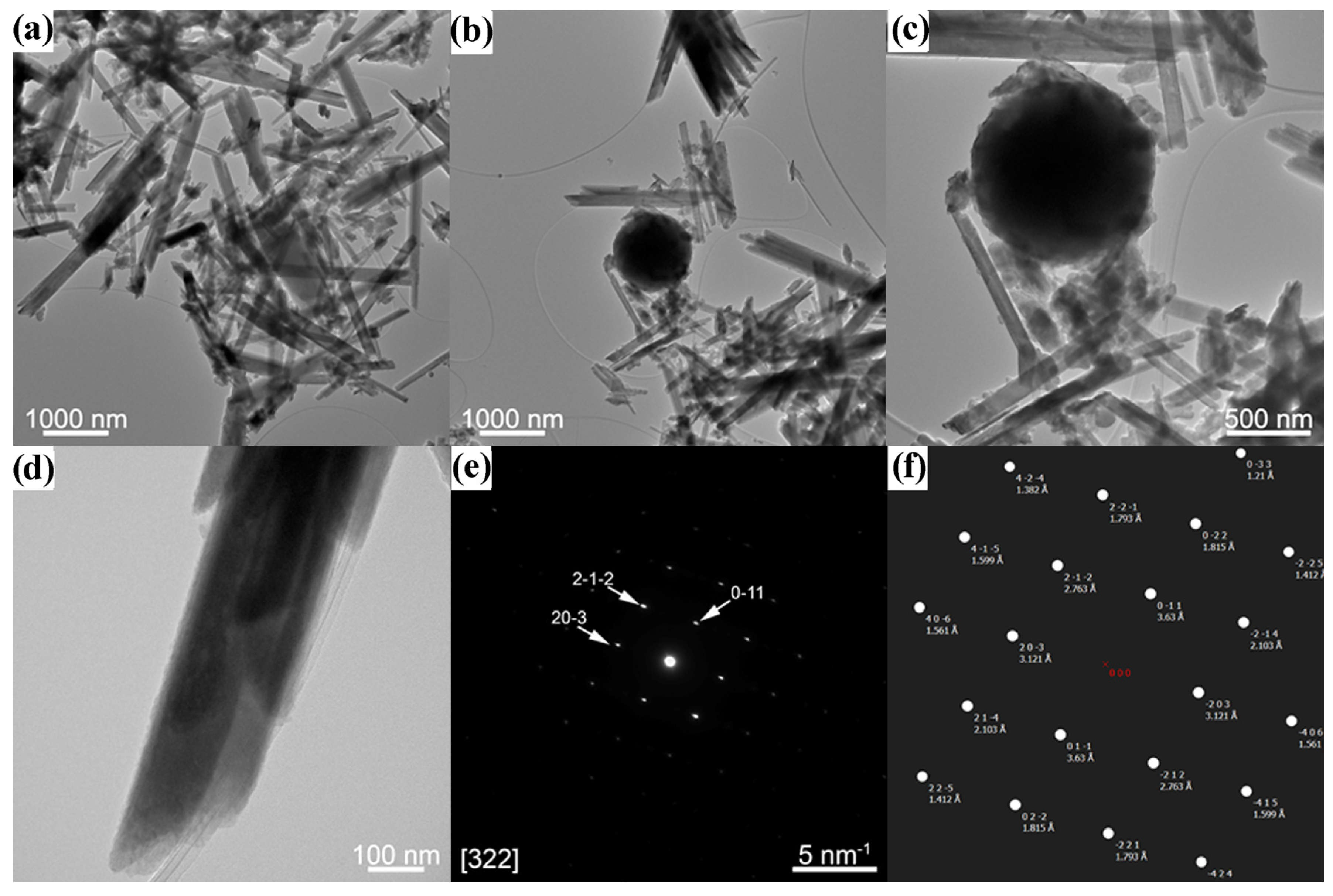
Three types of morphologies were identified by TEM analysis of the C5SS90 sample (Figure 12). The dominant one consists of large elongated particles whose lengths surpass 1000 nm with thicknesses below 200 nm. They have a larger length-to-thickness ratio than similar particles in the unsubstituted sample. The second type of particles are irregularly shaped nanoparticles with smaller dimensions (below 100 nm), agglomerated along the edges of elongated particles, and this morphology exists only in the presence of Cu. The overall content of elongated particles has increased. There is also a low amount of spherical nanoparticles that seem to be amorphous, which are mostly 100 nm in diameter. Spherical particles larger than 500 nm can be seen (Figure 12b,c), and the STEM mapping in Figure S5 shows them to be in the antimony-rich phase, explaining the bulk antimony observed by Raman analysis in some areas (Figure 5). EDX analysis (Figure S7) revealed significant traces of Cl in this region, but not in areas with elongated particles.
The SAED pattern of the elongated particle (Figure 12e) confirms its monocrystalline structure. The spots corresponding to the following lattice planes were measured: (20−3)—3.12 Å, (2−1−2)—2.76 Å and (0−11)—3.63 Å (these are indeed the (230), (221) and (101) planes indicated in Figure 3, only with different orders of the plane annotation in structure cards used in TEM analysis). The orientation of the Sb2S3 crystal in which these planes are visible simultaneously is in the [322] zone axis (Figure 12f).
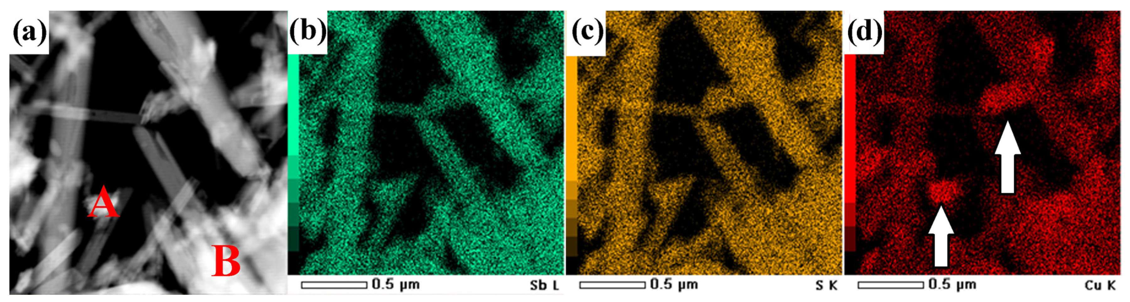
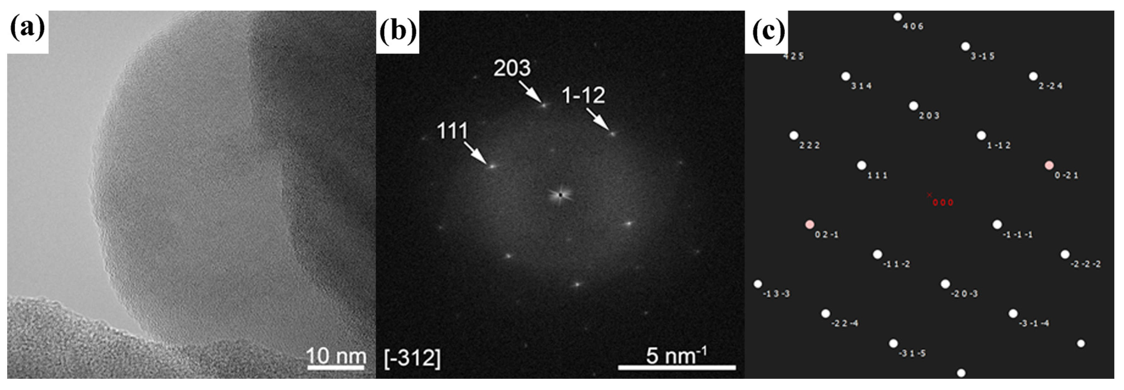
Copper was present in all particles at a similar level, and more than expected based on its doping level (according to EDX analysis presented in Figure S6). It is distributed quite uniformly, but it is possible to notice in the STEM mapping in Figure 13 that there are small regions where it is present in Cu-rich agglomerates (marked with arrows in Figure 13d), but along with Sb and S. The Cu-rich agglomerates are the smaller crystalline platelet-like particles, described as a second morphology. EDX analysis shows they exhibit roughly three times more Cu and somewhat less Sb and S than other particles (Figure S7), implying the presence of a Cu-rich secondary phase and an almost-matching CuSbS2 elemental composition. A well-oriented particle from a Cu-rich agglomerate (Figure 14) was determined to have an interplanar distance corresponding to the following lattice planes of the CuSbS2 crystal: (111) of 3.13 Å, (203) of 2.55 Å and (1−12) of 2.94 Å. The orientation that exhibits these planes is [−312] and the FFT measurement is confirmed by the comparison with the simulated electron diffraction pattern of the CuSbS2 crystal with the same orientation (Figure 14c).
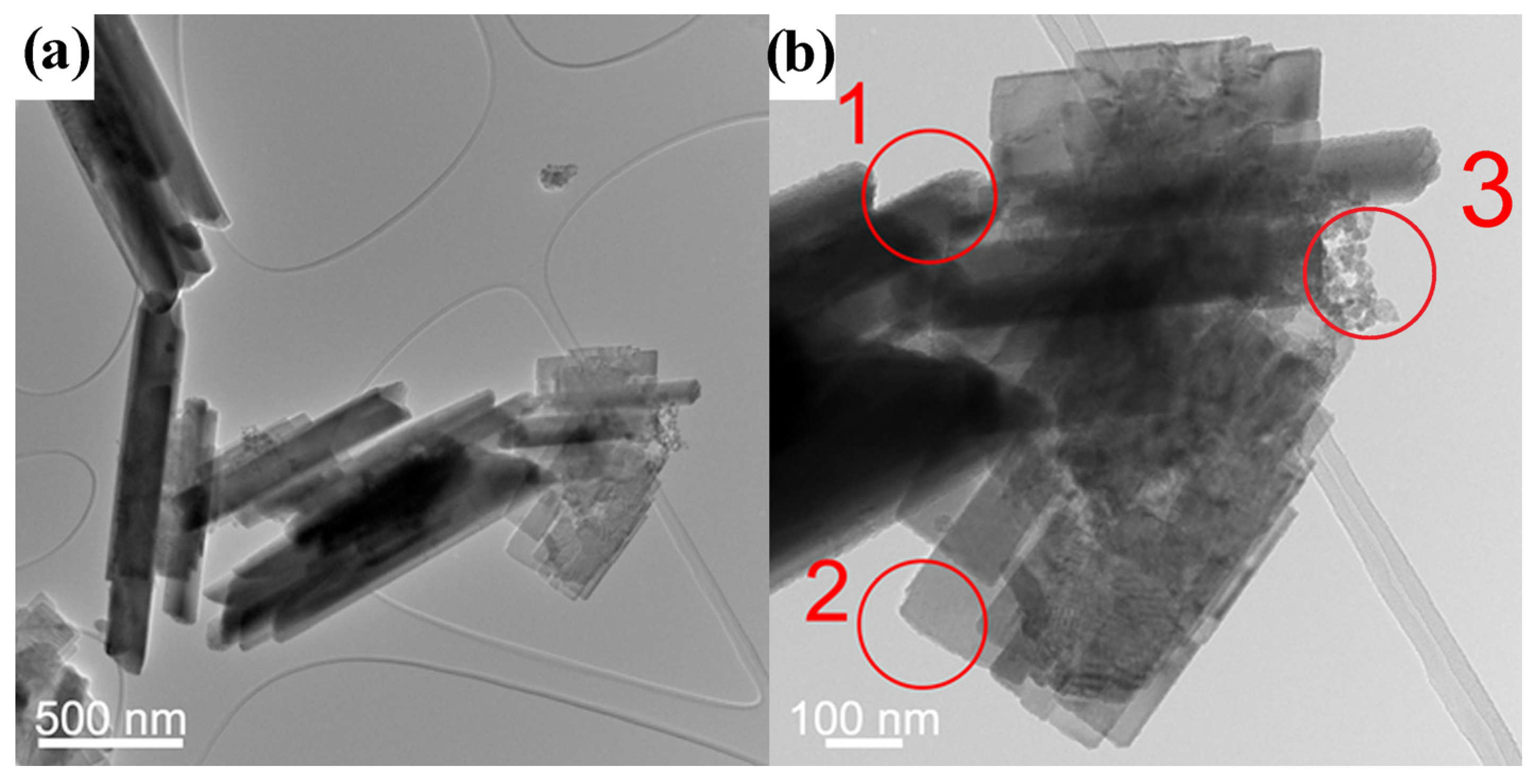
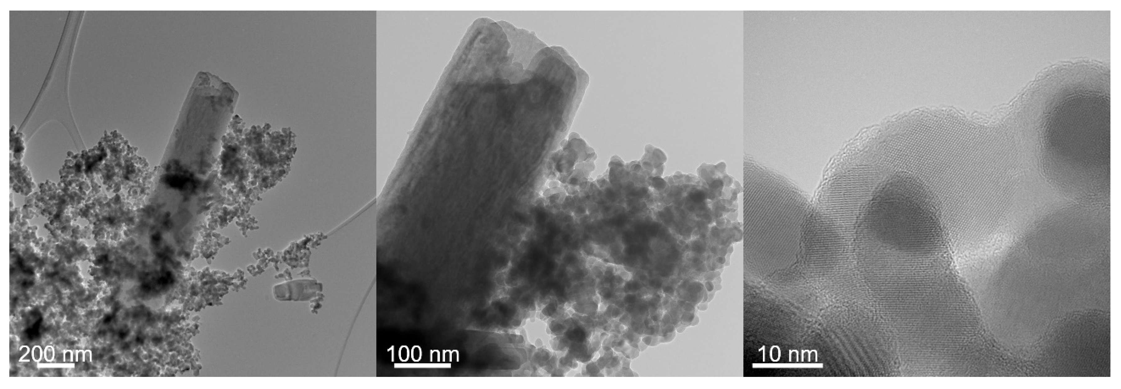
The TEM investigation of C10SS90 powders presented in Figure 15 revealed at least three morphologies. The most abundant are elongated particles (1000 nm × 200 nm), typical for Sb2S3, marked with 1 in Figure 15b, but there are also thicker rods present. The other main morphology (marked with 2 in Figure 15b) can be described as an almost rectangular sheet that has low thickness, which gives it a light contrast. Similar sheets can be seen to clearly overlap, a fact that suggests that its thickness along the view-axis is small. The other two dimensions are quite similar in size, reaching several hundred nanometers.
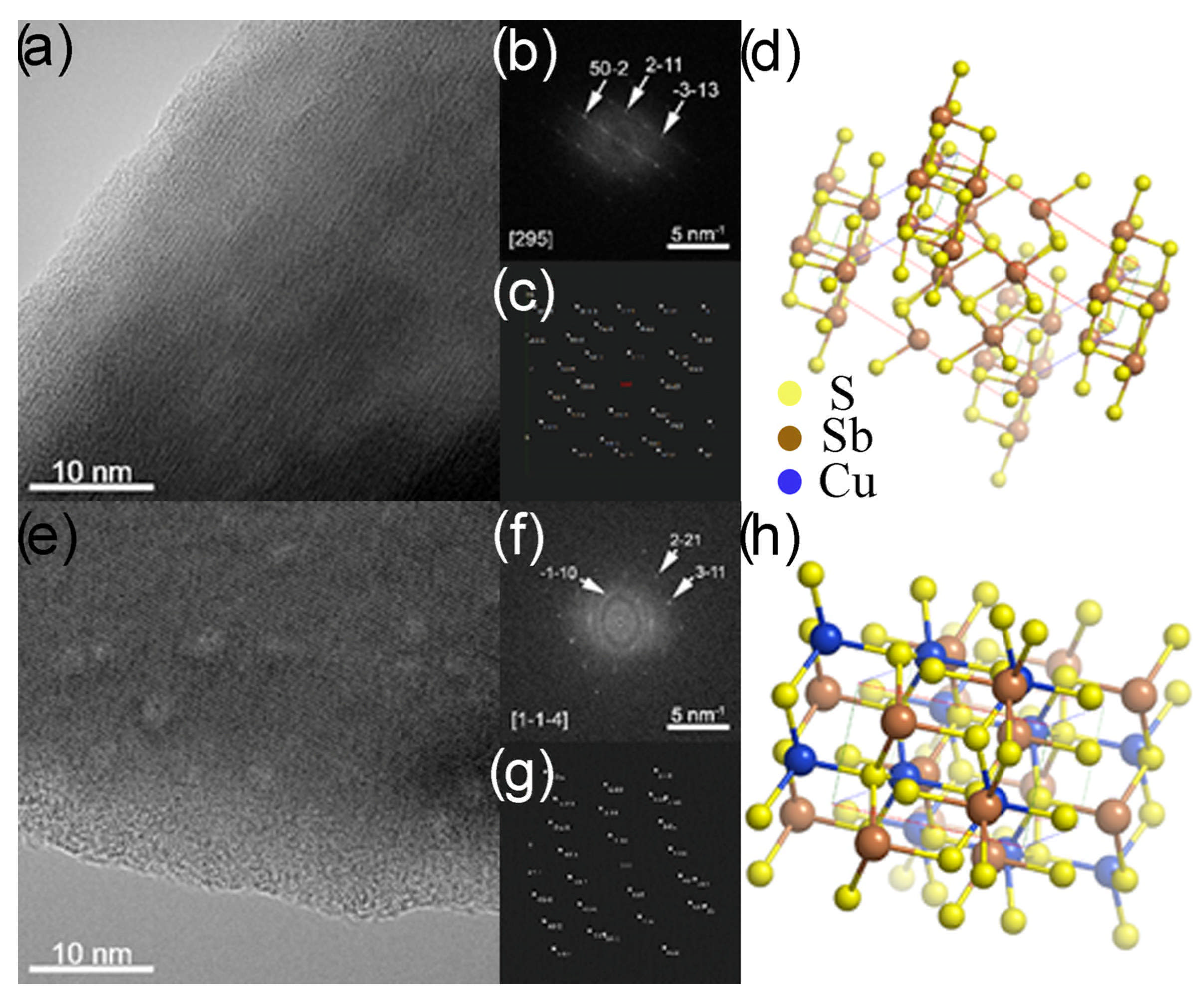
The HRTEM investigation of the two types of particles reveals that type 1 can be identified as Sb2S3, with its HRTEM image presented in Figure 16a. The Fourier transform of the image was performed (Figure 16b) and the spots were measured to correspond to the Sb2S3 lattice interplanar distances. The orientation of the Sb2S3 crystal in the image was deduced to be along the [295] zone axis, meaning it has a [295] Bravais lattice vector parallel to the electron beam. The comparison with the simulated diffraction pattern of a single crystal oriented along the same direction (Figure 16c) confirms that the phase is Sb2S3, with the structure represented in Figure 16d.
The analysis of type 2 sheets on HRTEM (Figure 16e) and the FFT pattern (Figure 16f) correspond to the interplanar distance of the CuSbS2 phase. The FFT pattern is compatible with the simulated diffraction pattern of a single-crystal CuSbS2 phase oriented along the [1−1−4] zone axis (Figure 16g), thus indicating that the type-two sheets are composed of CuSbS2, with the structural model shown in Figure 16h.
Type 3 morphologies are spherical nanoparticles observed in all the samples alongside the long crystalline rods and marked by area 3 in Figure 15b and Figure S8. These nanoparticles were scarcer in this sample and mostly amorphous with some crystallized areas (whose structure could not be determined). The diameter of spherical particles varies a lot, going from 10 to 100 nm.
Another much rarer morphological type (type 4) can be seen in Figure 17. It has an elongated, cylindrical shape with a length much larger than the width. The length has a dimension in the range of hundreds of nanometers while the width does not surpass 100 nm. This shape is similar to the rod-like particles of Sb2S3, though they are smaller and have a somewhat larger aspect ratio. The FFT analysis indicates that this particle has the structure of CuSbS2.
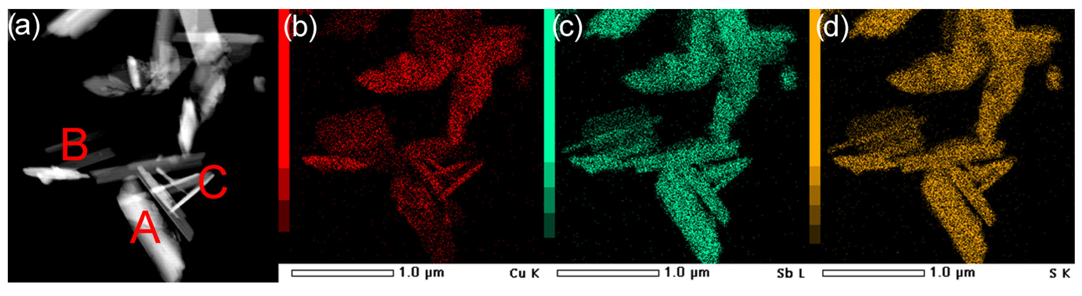
STEM EDX mapping was performed on an area that contained all described crystalline morphologies (Figure 18). The STEM image and the elemental maps corresponding to Cu, Sb and S are shown, confirming the almost completely uniform distribution of all three elements, with copper absent in some parts of the rod-like particles. EDX spectra of selected regions are presented in Figure S9. A type 1 elongated particle is represented in region A and its chemical composition shows that a small quantity of Cu (4.4 at. %) is present. The type 2 sheet particle in region B coincides with the composition of CuSbS2. Type 4 cylindrical CuSbS2 nanoparticles in region C had a somewhat smaller Cu/Sb ratio than the type 2 morphology, probably because the analyzed area was small and it overlapped with the Sb2S3 phase in the surrounding areas.
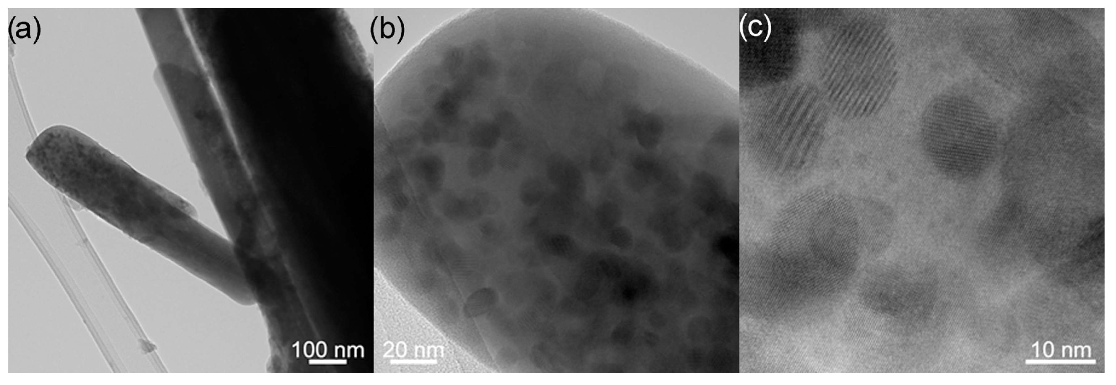
On some of the type 4 cylindrical CuSbS2 particles, interesting nanoparticulate regions were observed, as indicated in Figure 19. Numerous quasi-spherical, unidentified nanoparticles with diameters of around 10 nm are densely distributed over their surface.

2.4. XPS Analysis

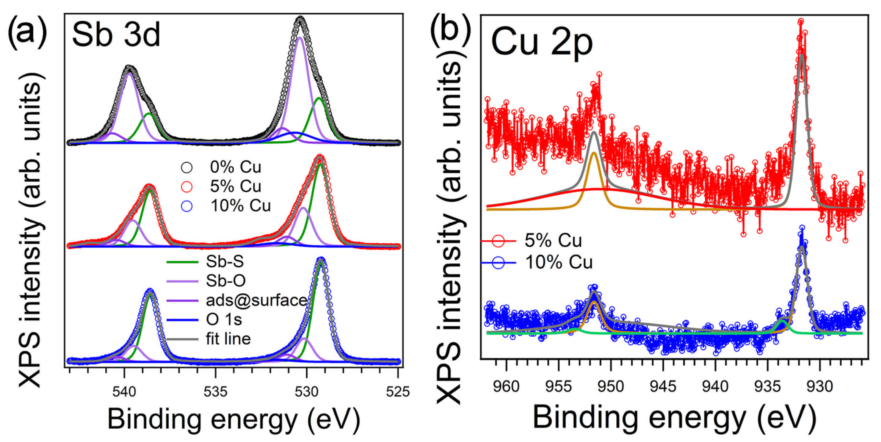
Survey spectra from XPS analysis of the synthesized powders are presented in Figure S10a, confirming the expected chemical composition. Core spectra of Sb 3d (Figure 20a) show that the undoped sample was highly oxidized and S-deficient, with a S/Sb ratio of 0.47. The Cu-substitution process had a beneficial effect in preventing the surface oxidation of the samples, and the S/Sb ratio got closer to the ideal ratios at 1.35 and 1.47 in C5SS90 and C10SS90, respectively. Interestingly, the Cu content in the surface layer was higher at lower substitution level as can be seen in Figure 20b. As oxides were not detected by XRD or Raman analyses, which possess much larger probing depths, it may be concluded that sulfides from a few of the top surface layers may succumb to oxidation, which should not have a drastic impact on the material as a whole, and this type of defects is often reported for Sb2S3 [29].
The presence of Cu on the surface of particles is not a true representation of the chemical composition of the bulk samples. When the substitution level was 5%, most of the Cu stayed close to the surface, while at 10% substitution, the distribution of Cu was mostly in the “bulk” of the powders, as can be seen in Figure 20b. This statement is supported by the VB spectra (Figure S10b), where the probing depth of XPS is the highest (considering the valence electrons have the highest kinetic energy). The shoulder, represented by a vertical gray line, shows Cu 4s states. Regarding the oxidation state of Cu 2p, in both the C5SS90 and C10SS90 samples, the dominant oxidation state of Cu is +1, and Cu2+ reaches the maximum of 15% in C10SS90.
The surfaces of the doped samples exhibit conductive behavior since the Fermi level is in the conduction band (the intersection of the other grey line represents the VB maxima in Figure S10b). The valence band maximum for Sb2S3 is at 0.1 eV, and the orange line represents the Fermi level.

2.5. Is It Possible to Reach a Pure CuSbS2 Composition?

Cu-substituted Sb2S3 powders contained a CuSbS2 secondary phase even when Cu was added in a concentration lower than the stoichiometric amount. This phase is a significant component, so it is more likely for the Sb-Cu-S system to form this phase than for Cu to substitute Sb in Sb2S3, at least by the synthesis method used here. But, what happens if Cu is added in the same amount as Sb? Would it be possible to obtain pure CuSbS2? With similar optical properties to Sb2S3, this phase is another interesting material for absorbers in photovoltaic devices [12,30]. For this purpose, we tried preliminary syntheses with the temperature, time and stoichiometry modified to get information about their influence on the structure. The synthesis was otherwise conducted in the same way as described in the Section 3.
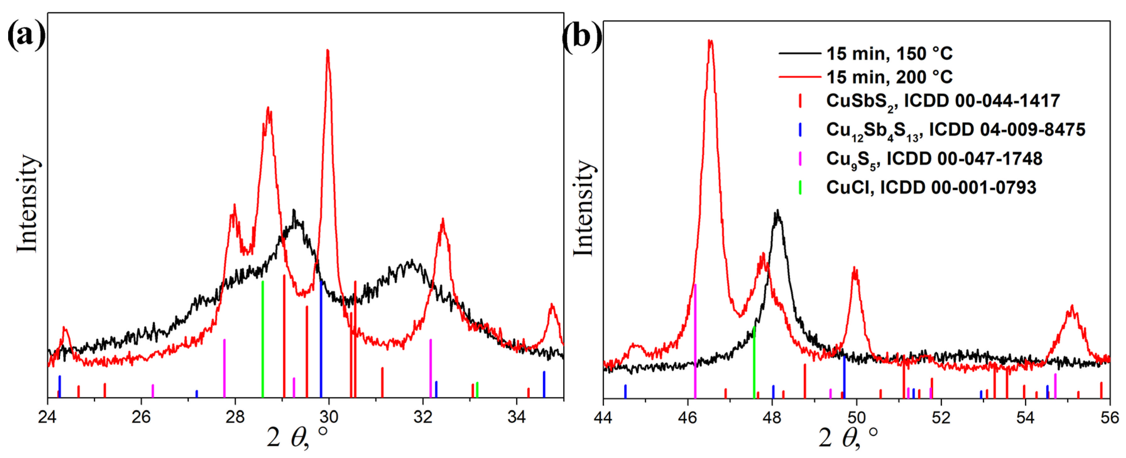
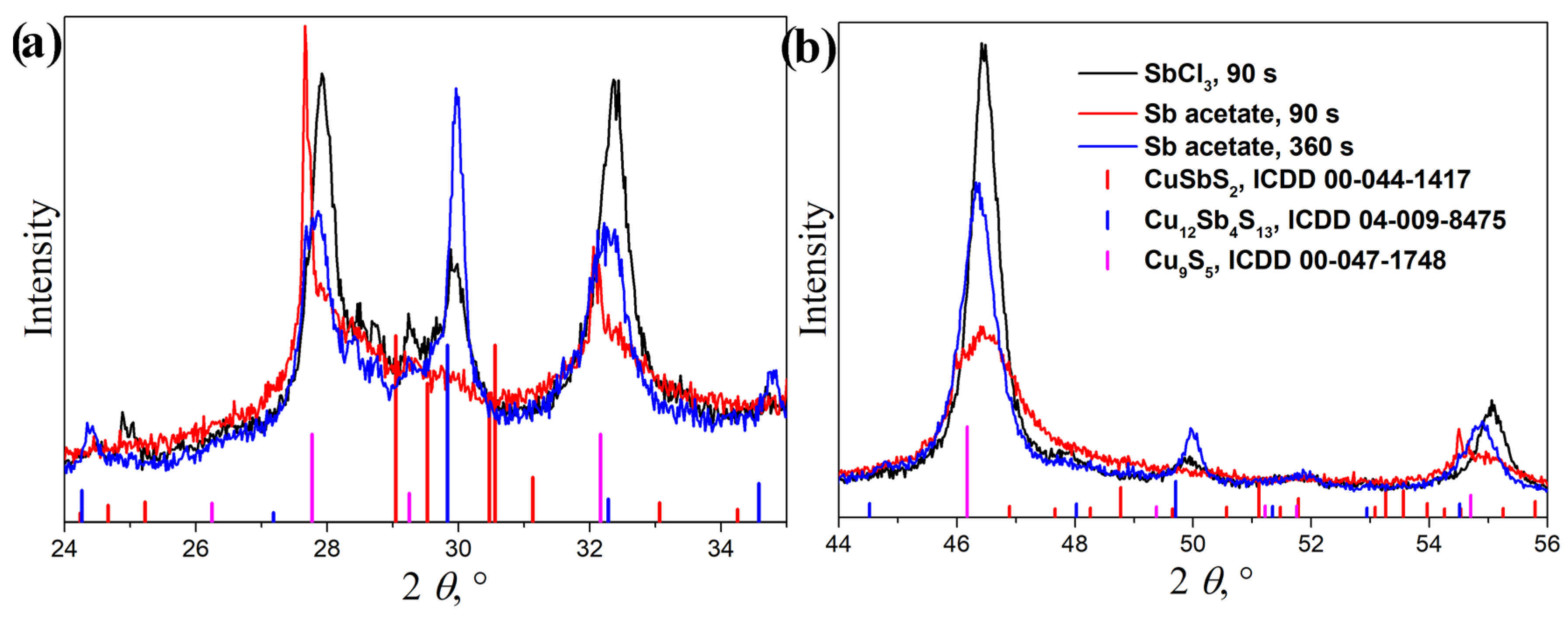
The kinetics of crystallization is similar to the synthesis of Sb2S3, meaning nucleation and growth are slow at 150 °C, where 15 min yields a dominantly amorphous product, while the same time at 200 °C allows a clear formation of CuCl, Cu9S5 and Cu12Sb4S13 as initial crystalline phases (Figure 21). When raising the reaction temperature to 230 °C (as for Sb2S3), the same level of crystallinity is reached in 1.5 min, but without the formation of CuCl, as can be seen in Figure 22.
Antimony acetate used as a Sb source to prevent the formation of chlorides made the crystallization slower and needed 6 min to develop a similar crystallinity result as SbCl3, showing a comparable effect of chloride ions, like that observed during the synthesis of Sb2S3. The results in Figure 22 imply that the absence of chlorides creates conditions where Cu9S5 is the phase that initially crystallizes and, over time, it partially recrystallizes into Cu12Sb4S13. This mechanism agrees with the one proposed by the research of Wang et al. identifying copper sulfide acts like nucleation seeds [31].
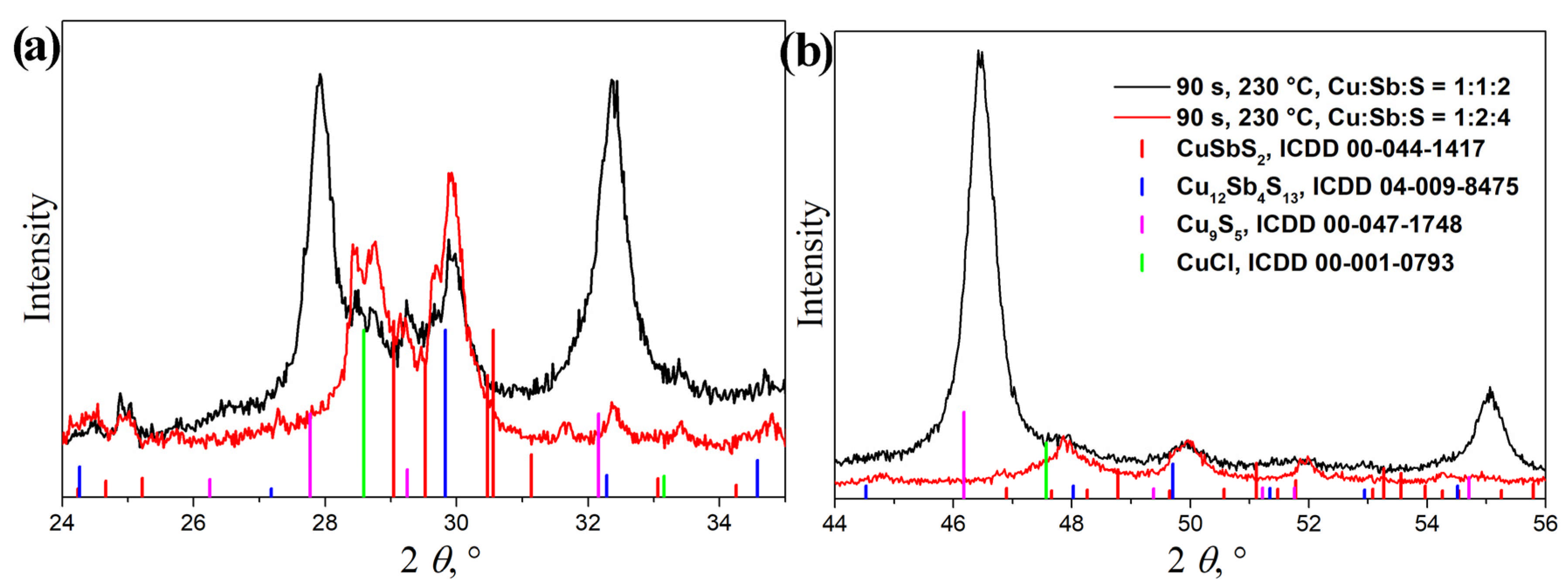
It becomes obvious that stoichiometrical composition (Sb:Cu = 1:1) does not produce CuSbS2, like it did when the Sb:Cu ratio was 9:1 (10% doping) or 19:1 (5% doping). The Cu9S5 phase, which initially crystallizes in Cu-rich conditions, prevents the subsequent development of CuSbS2. The use of deficient Cu(I) (Sb:Cu = 2:1) prevented the formation of the Cu9S5 phase, as seen in the diffraction pattern in Figure 23, but only avoided this step to form Cu12Sb4S13 faster, and did not influence the formation of a significant amount of the desired CuSbS2 phase at a Cu:Sb:S ratio of 1:2:4.
Structural analysis presented in Figure 21, Figure 22 and Figure 23 shows the formation of several crystalline phases, which were not all identified. The content of the desired CuSbS2 phase is very low, while Cu12Sb4S13 and Cu9S5 are the most prominent. The Cu-Sb-S system produces a lot of possible crystalline structures, and additional optimization is needed to define the conditions needed for the crystallization of the desired product. More preferable conditions for CuSbS2 crystallization were present in the non-stoichiometric content of Cu, Sb and S, which existed in 5 or 10% Cu-substituted Sb2S3 systems with Cu:Sb:S ratios of 1:9:15 and 1:19:30, where almost all added Cu was incorporated into CuSbS2. The literature shows that a low Cu content produces a CuSbS2 phase [32]. The study by Popovici et al. reported that the optimal Cu(II):Sb:S ratio to produce the highest CuSbS2 phase purity (73%) in spray-pyrolysis-synthesized films was 1:3.5:13, meaning that not only a 75% surplus Sb, but also a 550% surplus S was needed [7].
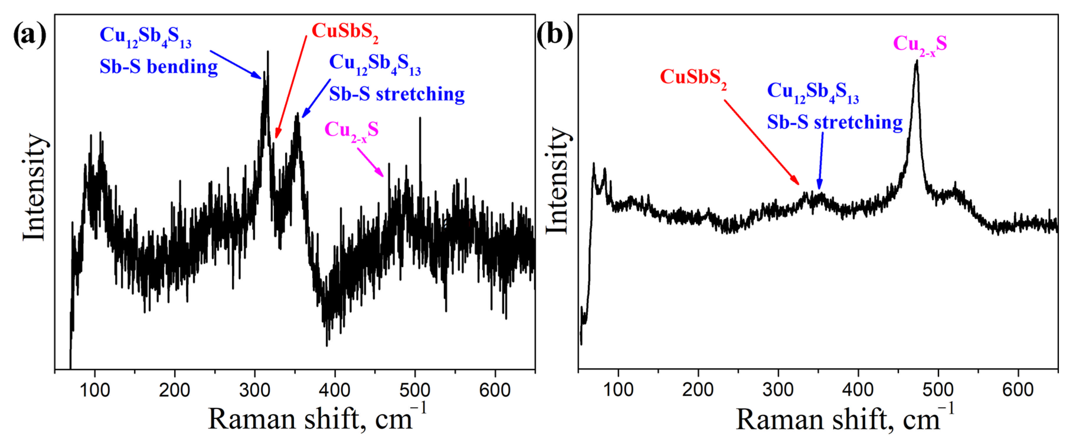
Raman analysis of CuSbS2 samples confirmed the findings of XRD analysis. After synthesis at 200 °C for 15 min, Sb-S stretching and bending peaks of the Cu12Sb4S13 phase at 350 and 315 cm−1 are the most pronounced (Figure 24). It is also possible to notice the Cu2−xS peak at 475 cm−1 [13,14]. Shorter times of synthesis were too amorphous to exhibit any peaks, and only weak contributions of Cu12Sb4S13 and Cu2−xS were noticeable. After 6 min at 230 °C, peaks are also undeveloped, with a dominant Cu2−xS phase but, in some regions, it is possible to notice a low presence of the CuSbS2 phase (peak at 332 cm−1).
The microstructural analysis of the sample synthesized for 6 min at 230 °C using Sb acetate in the stoichiometric mixture is presented in Figure 25. It shows the powder is composed of rod-like particles longer than 1000 nm and around 300 nm in diameter, and spherical nanoparticles of around 20 nm.

2.6. Optical Properties

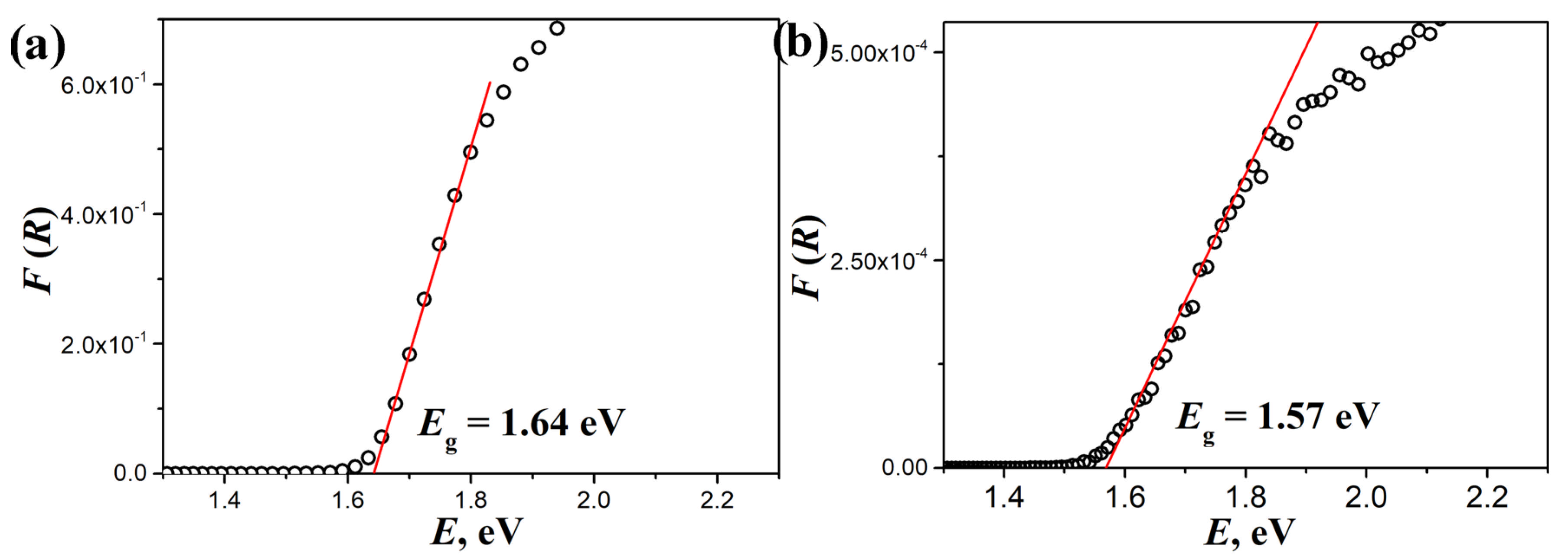
Optical band gaps of synthesized powders derived from the diffuse reflectance spectra are displayed in Table 1, with the fitted graphs presented for the samples SS90 and C10SS90 in Figure 26. Cu substitution has proven to slightly increase the absorption of the lower-energy spectra, so the band gap energy decreases, which is beneficial for sunlight-driven application. Attempts to synthesize CuSbS2 resulted in many phases, resulting in too-complex light-absorption properties to allow band gap determination.

3. Materials and Methods

The used starting chemicals were SbCl3 (99.0%, Alfa Aesar, Ward Hill, MA, USA), Sb(III) acetate (99.99%, Sigma Aldrich, St. Louis, MO, USA), Cu(I) acetate (97.0%, Sigma Aldrich) and elementary sulfur (99.999%, Alfa Aesar) as sources of antimony, copper and sulfur. Oleylamine (OlA) (≥98.0%, Sigma Aldrich), paraffin oil (Sigma Aldrich, puriss.) and ethylhexanoic acid (EHA) (≥99%, Aldrich Chemistry, St. Louis, MO, USA) were used as solvents, and hexane (95%, J.T. Baker, Phillipsburg, NJ, USA), benzene (99.93%, Lach-Ner, Neratovice, Czech Republic) and isopropanole (99.5%, J.T. Baker) were used to stop the reaction, help with precipitation and redispersion and wash the precipitate. Antimony and copper solutions in EHA preheated to 150 °C were injected into a solution of sulfur in paraffin oil and oleylamine preheated to 240 °C (reaction temperature around 230 °C) and precipitated for 45 or 90 s. After the reaction was stopped by the addition of hexane and isopropyl alcohol, the suspensions were cooled down and precipitated overnight. The precipitate was washed out in benzene, hexane and isopropanol to remove the remaining organics; each washing step was followed by centrifuge treatment for 10 min at 600 rpm. The procedure is explained in more detail in our previous studies [33,34]. The obtained powders were dried at 80 °C for 2 h and ground in an agate mortar. The obtained Sb2S3 powder samples were named by the substitution level and synthesis time, so 6 samples were present in total, as presented in Table 2: SS45 (Sb2S3 synthesized for 45 s), SS90 (Sb2S3 synthesized for 90 s), C5SS45 and C5SS90 (5% Cu(I)-doped Sb2S3 synthesized for 45 s and 90 s, respectively) and C10SS45 and C10SS90 (10% Cu(I)-doped Sb2S3 synthesized for 45 s and 90 s, respectively).
X-ray diffraction analysis was conducted using an Automated Multipurpose Powder X-ray Diffractometer XRDynamic 500 by Anton Paar GMBH, Graz, Austria, equipped with a Primux 3000 sealed-tube Cu X-ray source and a Pixos 2000 solid-state hybrid pixel detector. The XRD patterns of the samples were acquired using a Bragg–Brentano geometry in the continuous mode with a scan speed of 0.02°s−1 in a 2θ range from 10° to 140°.
Raman analysis was done employing a LabRAM HR Evolution Raman spectrometer (Horiba Jobin-Yvon, Montpellier, France) with a confocal microscope and a He–Ne laser at an excitation wavelength of 633 nm.
The microstructure and elemental distribution of the nanoparticles were analyzed using a JEOL-F200CF STEM apparatus (JEOL Ltd., Tokyo, Japan) equipped with an EDS system. A diluted particle solution was drop-casted onto nickel grids.
The high-resolution spectra for all of the core levels were measured by X-ray photoelectron spectroscopy (XPS) using a Kratos Ultra DLD spectrometer (Kratos Analytical, Manchester, UK) with a monochromatized Al Kα source (1486.6 eV). The source was operated at 144 W (12 mA and 12 kV), with 20 eV and 50 meV energy step resolutions. The charging effects were compensated using a flood gun and a correction of the binding energies to C=C contamination at 284.8 eV.
Optical properties of the synthesized powders were tested using a Shimadzu UV-2600 spectrophotometer (Shimadzu Corporation, Kyoto, Japan) equipped with an integrated sphere, measuring the reflectance of the layer of powder sample on a barium sulphate bed. Band gap energies were calculated using the Kubelka–Munk approximation (https://mmrc.caltech.edu/FTIR/Literature/Diff%20Refectance/Kubelka-Munk.pdf (accessed on 12 May 2026)).

4. Conclusions

Hot-injection synthesis was employed to synthesize copper-doped Sb2S3 nanoparticles of different morphologies than typical elongated rods of Sb2S3. Obtained powders were characterized to define the influence of the presence of Cu on their structure, microstructure and optical properties. Structural analysis implied that the metallic nature of Cu was too different from metalloid Sb in predominantly covalent Sb-S bonding to successfully substitute it in the Sb2S3 structure, despite suitable ionic radii. Elemental analysis of Cu-substituted samples revealed the spatial distribution of S, Sb and Cu uniformly distributed in all particles, with Cu-rich regions of the CuSbS2 phase existing without a change in S and Sb distributions. This contradicts the XRD results that show the substitution of Sb by Cu does not take place. One explanation may be that Cu is incorporated into the Sb2S3 phase on Sb positions, but sizes of Sb and Cu are similar enough to not disturb the structure at all. Another option is that Cu present in the amorphous phase uniformly covers the surface of Sb2S3 particles, showing a homogeneous distribution of Cu in those regions and a higher content in the particles of in CuSbS2 phase. The dominant microstructure of elongated rod-like particles of Sb2S3 and minor spherical amorphous nanoparticles remained the same in Cu-substituted samples, with the addition of nanoplatelets of CuSbS2. Cu substitution decreased the direct band gap, improving the absorption of the visible spectra. Different stoichiometries of the reactants were tested in the same synthesis method with the idea to obtain a pure CuSbS2 phase, which is another potential absorber material in photovoltaics, but these conditions were less favorable for the crystallization of the desired material. The precipitation of Cu is significantly faster than that of Sb, so excesses of Sb and S are needed to produce the CuSbS2 phase, creating a lot of unreacted dissolved ions in the liquid phase. The poor solubility of copper chlorides in organic solvents introduced another secondary phase, which may be prevented by using Sb acetate as the source of Sb, though the absence of chlorides also has a retarding impact on the kinetics of precipitation. Our future work should optimize synthesis conditions and reactant ratios to explore two possible directions of research: (1) the production of crystalline Sb2S3 particles with a reduced aspect ratio, and (2) the production of pure CuSbS2 powder, both to be tested as a light absorber in photovoltaic devices.

Supplementary Materials

The following supporting information can be downloaded at: https://www.mdpi.com/article/10.3390/ijms27167406/s1.

Author Contributions

Conceptualization, I.V. and N.I.; methodology, N.I., C.R. and A.E.B.; investigation, N.I., C.R. and A.E.B.; resources, I.V. and A.C.G.; data curation, A.C.G.; writing—original draft preparation, N.I., I.V. and C.R.; writing—review and editing, I.V. and A.C.G.; visualization, A.C.G.; supervision, I.V. All authors have read and agreed to the published version of the manuscript.

Funding

This work was supported by the Ministry of Science, Technological Development and Innovation of the Republic of Serbia (Contract No. 451-03-33/2026-03/200017) and Romanian National Authority for Research (Autoritatea Națională pentru Cercetare) through the Core Programme PC3-PN23080303 project, and by UEFISCDI (Unitatea Executivă pentru Finanțarea Învățământului Superior, a Cercetării, Dezvoltării și Inovării) through the ERANET-M-3-ERANET Ligthcell project (contract No. 19/15.03.2024) and PN-IV-PCB-RO-MD Empower project (contract No. 28PCBROMD/22.09.2025). All authors acknowledge the COST Action Research and International Networking project “Emerging Inorganic Chalcogenides for Photovoltaics (Renew-PV),” CA21148, supported by COST (European Cooperation in Science and Technology), and the Renew-PV grant awarded to N.I. to perform a Short-Term Scientific Mission (STSM) at NIMP. The XPS measurements were performed using the Romanian [M85.1] National Interest Setup “System of complex XPS/ESCA installations and research using synchrotron radiation”.

Institutional Review Board Statement

Not applicable.

Informed Consent Statement

Not applicable.

Data Availability Statement

The raw data supporting the conclusions of this article will be made available by the authors on request.

Conflicts of Interest

The authors declare no conflicts of interest.

References

  1. Kondrotas, R.; Chen, C.; Tang, J. Sb2S3 Solar Cells. Joule 2018, 2, 857–878. [Google Scholar] [CrossRef] [Scilit]
  2. Chen, X.; Shu, X.; Zhou, J.; Wan, L.; Xiao, P.; Fu, Y.; Ye, J.; Huang, Y.-T.; Yan, B.; Xue, D.; et al. Additive engineering for Sb2S3 indoor photovoltaics with efficiency exceeding 17%. Light-Sci. Appl. 2024, 13, 281. [Google Scholar] [CrossRef] [Scilit] [PubMed]
  3. Wang, X.; Li, Z.; Kavanagh, S.R.; Ganose, A.M.; Walsh, A. Lone pair driven anisotropy in antimony chalcogenide semiconductors. Phys. Chem. Chem. Phys. 2022, 24, 7195–7202, Correction in Phys. Chem. Chem. Phys. 2023, 25, 25055. [Google Scholar] [CrossRef] [Scilit] [PubMed]
  4. Farhana, M.A.; Manjceevan, A.; Bandara, J. Recent advances and new research trends in Sb2S3 thin film based solar cells. J. Sci. Adv. Mater. Devices 2023, 8, 100533. [Google Scholar] [CrossRef] [Scilit]
  5. Validžić, I.L.; Mitrić, M. Colloidal synthesis of Sb2S3 nanorods/bars with strong preferred orientation. Mater. Lett. 2011, 65, 1919–1922. [Google Scholar] [CrossRef] [Scilit]
  6. Validžić, I.L.; Abazović, N.D.; Mitrić, M. Growth of Sb2S3 Nanowires Synthesized by Colloidal Process and Self-Assembly of Amorphous Spherical Sb2S3 Nanoparticles in Wires Formation. Met. Mater. Int. 2012, 18, 989–995. [Google Scholar] [CrossRef] [Scilit]
  7. Validžić, I.; Popović, M.; Potočnik, J.; Graf, C.; Joschko, M.; Kuznetsova, Y.A.; Zatsepin, D.A. Amorphous non-doped and Se-, Cu-, and Zn-doped Sb2S3 nanoparticles prepared by a hot-injection method: Bandgap tuning and possible observation of the quantum size effect. J. Nanopart. Res. 2023, 25, 48. [Google Scholar] [CrossRef] [Scilit]
  8. Janošević, V.; Mitrić, M.; Bundaleski, N.; Rakočević, Z.; Validžić, I. High-efficiency Sb2S3-based hybrid solar cell at low light intensity: Cell made of synthesized Cu and Se-doped Sb2S3. Prog. Photovolt. Res. Appl. 2016, 24, 704–715. [Google Scholar] [CrossRef] [Scilit]
  9. Salinas-Beltran, S.; Gaitan-Arevalo, J.; Gonzalez, L.A. Improvement of the photoelectrical properties of chemical bath-deposited Sb2S3 thin films with low copper doping. J. Mater. Sci. Mater. Electron. 2024, 35, 458. [Google Scholar] [CrossRef] [Scilit]
  10. Balnan, I. Structural and Photovoltaic Enhancements in Cu-doped Sb2S3 Thin Films via Chemical Bath Deposition. MAS J. Appl. Sci. 2025, 10, 643–655. [Google Scholar]
  11. Popovici, I.; Duta, A. Tailoring the Composition and Properties of Sprayed CuSbS2 Thin Films by Using Polymeric Additives. Int. J. Photoenergy 2012, 2012, 962649. [Google Scholar] [CrossRef] [Scilit][Green Version]
  12. Welch, A.W.; Zawadzki, P.P.; Lany, S.; Wolden, C.A.; Zakutayev, A. Self-regulated growth and tunable properties of CuSbS2 solar absorbers. Sol. Energy Mater. Sol. Cells 2015, 132, 499–506. [Google Scholar] [CrossRef] [Scilit]
  13. Sivagami, A.D.; Biswas, K.; Sarma, A. Orthorhombic CuSbS2 nanobricks: Synthesis and its photo responsive behaviour. Mater. Sci. Semicond. Process. 2018, 87, 69–76. [Google Scholar] [CrossRef] [Scilit]
  14. Prem Kumar, D.S.; Ren, M.; Osipowicz, T.; Mallik, R.C.; Malar, P. Tetrahedrite (Cu12Sb4S13) thin films for photovoltaic and thermoelectric Applications. Sol. Energy 2018, 174, 422–430. [Google Scholar] [CrossRef] [Scilit]
  15. Pal, M.; Torres Luna, Y.; Silva González, R.; Mathews, N.R.; Paraguay-Delgado, F.; Pal, U. Phase controlled synthesis of CuSbS2 nanostructures: Effect of reaction conditions on phase purity and morphology. Mater. Des. 2017, 136, 165–173. [Google Scholar] [CrossRef] [Scilit]
  16. Zhang, M.; Wang, C.; Chen, C.; Tang, J. Recent progress in the research on using CuSbS2 and its derivative CuPbSbS3 as absorbers in case of photovoltaic devices. Front. Optoelectron. 2021, 14, 450–458. [Google Scholar] [CrossRef] [Scilit] [PubMed]
  17. Edley, M.E.; Opasanont, B.; Conley, J.T.; Tran, H.; Smolin, S.Y.; Li, S.; Dillon, A.D.; Fafarman, A.T.; Baxter, J.B. Solution processed CuSbS2 films for solar cell applications. Thin Solid Films 2018, 646, 180–189. [Google Scholar] [CrossRef] [Scilit]
  18. Moosakhani, S.; Alvani, A.A.S.; Mohammadpour, R.; Hannula, P.-M.; Ge, Y.; Hannula, S.-P. Platelet CuSbS2 particles with a suitable conduction band position for solar cell applications. Mater. Lett. 2018, 215, 157–160. [Google Scholar] [CrossRef] [Scilit]
  19. Suehiro, S.; Horita, K.; Yuasa, M.; Tanaka, T.; Fujita, K.; Ishiwata, Y.; Shimanoe, K.; Kida, T. Synthesis of Copper-Antimony-Sulfide Nanocrystals for Solution-Processed Solar Cells. Inorg. Chem. 2015, 54, 7840–7845. [Google Scholar] [CrossRef] [Scilit] [PubMed]
  20. Obare, N.; Isoe, W.; Nalianya, A.; Mageto, M.; Odari, V. Numerical Study of copper antimony sulphide (CuSbS2) solar cell by SCAPS-1D. Heliyon 2024, 10, e26896. [Google Scholar] [CrossRef] [Scilit] [PubMed]
  21. Lian, W.; Jiang, C.; Yin, Y.; Tang, R.; Li, G.; Zhang, L.; Che, B.; Chen, T. Revealing composition and structure dependent deep-level defect in antimony trisulfide photovoltaics. Nat. Commun. 2021, 12, 3260. [Google Scholar] [CrossRef] [Scilit] [PubMed]
  22. Wang, J.; Qiao, Y.; Wang, T.; Yu, H.; Feng, Y.; Li, L. Two-dimensional (2D) amorphous antimony (III) trisulfide nanosheets: Synthesis, photoelectronic property and their transformation to crystalline 1D micro/nanorods. Inorg. Chem. Commun. 2018, 92, 110–114. [Google Scholar] [CrossRef] [Scilit]
  23. Shannon, R.D. Revised Effective Ionic Radii and Systematic Studies of interatomic distances in Halides and chalcogenides. Acta Cryst. 1976, A32, 751–767. [Google Scholar] [CrossRef] [Scilit]
  24. Lebarstard, C.; Hassam, C.; Suzuki, T.; Uchikoshi, T.; Thimont, Y.; Berthebaud, D. Investigation of Silver and Copper Doping on Antimony Sulfide Thin Films Obtained by Electrophoretic Deposition. J. Phys. Chem. C 2024, 128, 18093–18101. [Google Scholar] [CrossRef] [Scilit]
  25. DeAngelis, A.D.; Kemp, K.C.; Gaillard, N.; Kim, K.S. Antimony(III) Sulfide Thin Films as a Photoanode Material in Photocatalytic Water Splitting. ACS Appl. Mater. Interfaces 2016, 8, 8445–8451. [Google Scholar] [CrossRef] [Scilit] [PubMed]
  26. Ismail, M.M.; Vigneshwaran, J.; Arunbalaji, S.; Mani, D.; Arivanandhan, M.; Jose, S.P.; Jayavel, R. Antimonene nanosheets with enhanced electrochemical performance for energy storage applications. Dalton Trans. 2020, 49, 13717. [Google Scholar] [CrossRef] [Scilit] [PubMed]
  27. Efthimiopoulos, I.; Buchan, C.; Wang, Y. Structural properties of Sb2S3 under pressure: Evidence of an electronic topological transition. Sci. Rep. 2016, 6, 24246. [Google Scholar] [CrossRef] [Scilit] [PubMed]
  28. Zhou, W.; Thomas, J.M. HRTEM surface profile imaging of solids. Curr. Opin. Solid State Mater. Sci. 2001, 5, 75–83. [Google Scholar] [CrossRef] [Scilit]
  29. Kavya, D.M.; Sudhakar, Y.N.; Timoumi, A.; Raviprakash, Y. Thickness-dependent performance of antimony sulfide thin films as a photoanode for enhanced photoelectrochemical water splitting. RSC Adv. 2025, 15, 13691–13702. [Google Scholar] [CrossRef] [Scilit] [PubMed]
  30. Yang, B.; Wang, L.; Han, J.; Zhou, Y.; Song, H.; Chen, S.; Zhong, J.; Lv, L.; Niu, D.; Tang, J. CuSbS2 as a Promising Earth-Abundant Photovoltaic Absorber Material: A Combined Theoretical and Experimental Study. Chem. Mater. 2014, 26, 3135–3143. [Google Scholar] [CrossRef] [Scilit]
  31. Wang, W.; Hao, L.; Zhi, G.; Lin, Q.; Tang, Z. Investigation on preparation and formation mechanism of copper antimony sulphide particles by microwave irradiation. Micro Nano Lett. 2018, 13, 1036–1039. [Google Scholar] [CrossRef] [Scilit]
  32. Makin, F.; Alam, F.; Buckingham, M.A.; Lewis, D.J. Synthesis of ternary copper antimony sulfide via solventless thermolysis or aerosol assisted chemical vapour deposition using metal dithiocarbamates. Sci. Rep. 2022, 12, 5627. [Google Scholar] [CrossRef] [Scilit] [PubMed]
  33. Joschko, M.; Wafo, F.Y.F.; Malsi, C.; Kisić, D.; Validžić, I.; Graf, C. Revealing the formation mechanism and band gap tuning of Sb2S3 nanoparticles. Beilstein J. Nanotechnol. 2021, 12, 1021–1033. [Google Scholar] [CrossRef] [Scilit] [PubMed]
  34. Ilić, N.; Validžić, I.; Barudžija, T.; Stevanović, S. Hot injection synthesis parameters effects on the structure, crystallinity, microstructure and optical properties of Sb2S3 nanopowders. Mater. Sci. Eng. B-Adv. 2026, 326, 119165. [Google Scholar] [CrossRef] [Scilit]
Scheme 1. Structures of orthorhombic Pnma: (a) Sb2S3 and (b) CuSbS2 structures drawn using the open access database The materials project (https://next-gen.materialsproject.org/, accessed on 12 August 2026).
Ijms 27 07406 sch001
Figure 1. XRD diffraction patterns of (a) SS45 and (b) SS90 powders.
Ijms 27 07406 g001
Figure 2. XRD patterns of SS45 and C10SS45 (a) and enlarged part of the patterns for 2θ between 27.5 and 30.5° (b).
Ijms 27 07406 g002
Figure 3. XRD patterns of SS90, C5SS90 and C10SS90 powders.
Ijms 27 07406 g003
Figure 4. Enlarged regions of interest of XRD patterns of SS90, C5SS90 and C10SS90 powders with linear (a) and logarithmic (b) intensity scales.
Ijms 27 07406 g004
Figure 5. Raman spectra of (a) SS45; (b) SS90.
Ijms 27 07406 g005
Figure 6. Raman spectra of (a) C5SS90; (b) C10SS90.
Ijms 27 07406 g006
Figure 7. TEM images of SS45 powder at (a) 7000×, (b) 10,000×, and (c) 22,000× magnifications.
Ijms 27 07406 g007
Figure 8. (a) TEM images of the end of the Sb2S3 microrod from the SS45 sample, (b) selected area diffraction pattern and (c) simulated diffraction pattern oriented along the [102] zone axis.
Ijms 27 07406 g008
Figure 9. TEM images of the conjoined spherical nanoparticles in the SS45 sample (a); STEM image and EDX elemental analysis showing the Sb and S distribution (b).
Ijms 27 07406 g009
Figure 10. (a) Low-magnification TEM images of the SS90 sample, (b) HRTEM image of the elongated particle, (c) FFT pattern corresponding to it, (d) simulated diffraction pattern of a Sb2S3 crystal oriented along the [−235] zone axis and (e) structural model of the Sb2S3 crystal oriented as in the HRTEM image.
Ijms 27 07406 g010
Figure 11. (a) TEM images of the spherical particle region of the SS90 nanopowder, with indicated nanocrystalline (red) and porous-like (blue) features; (b) HRTEM image in the red circled area; (c) FFT pattern of the HRTEM image; (d) simulated diffraction pattern of the Sb2S3 crystal oriented along the [2−1−3] crystallographic direction and (e) STEM dark-field image of the SS90 power, with elemental distribution maps of Sb and S.
Ijms 27 07406 g011
Figure 12. (ad) TEM images of the C5SS90 sample at different magnifications with (e) selected area diffraction patterns of regions observed at (d), and (f) simulated diffraction pattern of the Sb2S3 crystal oriented along the [322] zone axis.
Ijms 27 07406 g012
Figure 13. STEM mapping of the C5SS90 powder: the selected area microstructure with marked A and B characteristic regions (a), and mappings of Sb (b), S (c) and Cu (d) (arrows are indicating the Cu-rich regions).
Ijms 27 07406 g013
Figure 14. (a) HRTEM images of a well-oriented particle from the Cu-rich agglomerate, (b) FFT images corresponding to it and (c) simulated diffraction pattern of CuSbS2 crystal oriented along the [−312] zone axis.
Ijms 27 07406 g014
Figure 15. TEM images of C10SS90 powder (a), with enlarged section with marked morphologies of rod particles (1), platelets (2) and spherical nanoparticles (3) (b).
Ijms 27 07406 g015
Figure 16. HRTEM images of the elongated particle (a) and sheet particle (e) of C10SS90 powder; Fourier transform (b,f); simulated diffraction pattern of Sb2S3 along the [295] zone axis (c); structural model of Sb2S3 oriented along the [295] axis (d); simulated diffraction pattern of CuSbS2 along the [1−1−4] zone axis (g) and structural model of CuSbS2 along the [1−1−4] zone axis (h).
Ijms 27 07406 g016
Figure 17. (a) TEM images and (b) HRTEM images of type 4 particles of C10SS90 powder with (c) FFT pattern corresponding to image (b) in which the interplanar distances belonging to the CuSbS2 phase were measured.
Ijms 27 07406 g017
Figure 18. STEM EDX mapping of C10SS90 powder: (a) mapped area with indicated characteristic A, B and C regions; (b) Cu, (c) Sb and (d) S mapping.
Ijms 27 07406 g018
Figure 19. Lower-magnification TEM images of C10SS90 powder (a) and TEM images of the same area at higher magnifications (b,c).
Ijms 27 07406 g019
Figure 20. Core XPS spectra of the Sb 3d (a) and Cu 2p (fitted with orange line) (b) of SS90, C5SS90 and C10SS90 powders.
Ijms 27 07406 g020
Figure 21. Influence of hot-injection temperature: XRD patterns of CuSbS2 samples synthesized for 15 min at 150 °C and 200 °C, presented in two zoomed-in 2θ domains: 24–35° (a) and 44–56° (b).
Ijms 27 07406 g021
Figure 22. XRD patterns of CuSbS2 samples synthesized for 90 s using SbCl3, 90 s using Sb acetate and 360 s using Sb acetate, all at 230 °C, presented in two zoomed-in 2θ domains: 24–35° (a) and 44–56° (b).
Ijms 27 07406 g022
Figure 23. Influence of ion stoichiometry (Cu:Sb:S ratios of 1:1:2 and 1:2:4) on structure, presented in two zoomed-in 2θ domains: 24–35° (a) and 44–56° (b).
Ijms 27 07406 g023
Figure 24. Raman spectra of Sb2S3 synthesized for (a) 15 min at 200 °C (from SbCl3) and (b) 6 min at 230 °C (from Sb acetate).
Ijms 27 07406 g024
Figure 25. TEM images of CuSbS2 powder made from the stoichiometric mixture.
Ijms 27 07406 g025
Figure 26. Kubelka–Munk-function fitted direct band gaps of SS90 (a) and C10SS90 (b).
Ijms 27 07406 g026
Table 1. Direct and indirect band gaps of synthesized materials.
SampleEg, Direct, eVEg, Indirect, eVDirect/Indirect
SS452.041.79Indirect
SS901.641.52Direct
C5SS901.671.50Direct
C10SS901.571.42Direct
“CuSbS2Unreliable, ~2.0Direct
Table 2. Preview of the samples based on synthesis time and copper substitution level.
Time, sCopper Substitution Level, mol %
0510
45SS45C5SS45C10SS45
90SS90C5SS90C10SS90
Disclaimer/Publisher’s Note: The statements, opinions and data contained in all publications are solely those of the individual author(s) and contributor(s) and not of MDPI and/or the editor(s). MDPI and/or the editor(s) disclaim responsibility for any injury to people or property resulting from any ideas, methods, instructions or products referred to in the content.