Review

Recent Advances in Inverted Perovskite Solar Cells: Designing and Fabrication

1
Engineering Research Center for Hydrogen Energy Materials and Devices, College of Rare Earths, Jiangxi University of Science and Technology, Ganzhou 341000, China
2
Faculty of Materials Metallurgy and Chemistry, Jiangxi University of Science and Technology, Ganzhou 341000, China
3
College of Chemistry, Jilin University, Changchun 130012, China
*
Authors to whom correspondence should be addressed.
Int. J. Mol. Sci. 2022, 23(19), 11792; https://doi.org/10.3390/ijms231911792
Submission received: 30 August 2022 / Revised: 25 September 2022 / Accepted: 28 September 2022 / Published: 4 October 2022
(This article belongs to the Special Issue Materials for Energy Applications 2.0)

Abstract

:
Inverted perovskite solar cells (PSCs) have been extensively studied by reason of their negligible hysteresis effect, easy fabrication, flexible PSCs and good stability. The certified photoelectric conversion efficiency (PCE) achieved 23.5% owing to the formed lead−sulfur (Pb−S) bonds through the surface sulfidation process of perovskite film, which gradually approaches the performance of traditional upright structure PSCs and indicates their industrial application potential. However, the fabricated devices are severely affected by moisture, high temperature and ultraviolet light due to the application of organic materials. Depending on nitrogen, cost of protection may increase, especially for the industrial production in the future. In addition, the inverted PSCs are found with a series of issues compared with the traditional upright PSCs, such as nonradiative recombination of carriers, inferior stability and costly charge transport materials. Thus, the development of inverted PSCs is systematically reviewed in this paper. The design and fabrication of charge transport materials and perovskite materials, enhancement strategies (e.g., interface modification and doping) and the development of all−inorganic inverted devices are discussed to present the indicator for development of efficient and stable inverted PSCs.

1. Introduction

At present, humanity is faced with serious energy and environmental issues [1,2]. Even if timely energy conservation measures are taken, the world energy demand is expected to increase triple by 2050 [3]. In addition, the consumption of fossil fuels produces some nasty side effects, including air pollution and greenhouse effects [4,5]. Solar energy is a renewable clean energy [6,7]. Thus, solar cells, as the devices that convert sunlight into electricity directly, are considered as one of the efficient approaches to satisfying the appetite for clean energy in the future [8,9]. Until now, silicon (Si) solar cells possess the best photovoltaic efficiency and dominate the solar panel market [10,11]. Nevertheless, the popularity of Si solar cells is restricted by reason of their huge expense and serious pollution.
Perovskite solar cells (PSCs), as a novel type of solar cells, have received a lot of attention and research because of their wide light absorption range, high optical absorption coefficient and high carrier mobility of metal halide−based perovskite materials. With a few short years, PSCs have made a significant breakthrough, and the certified PCE has already achieved 25.5% [12]. To date, most PSCs have been constructed in the traditional upright structure. However, the traditional upright structure devices suffer from serious hysteresis effects and poor stability. Moreover, most of the traditional upright devices consist of a metal oxides electron−transport layer (ETL) with high sintering temperature, which leads to difficulty in achieving the development of flexible PSCs. Although numerous strategies, including surface passivation [13,14,15], interface engineering [16,17,18,19,20], doping [21,22,23,24,25], cross−linking of the perovskite film [26] and so on, have been developed to mitigate these issues, the PCE of PSCs is still well below the Shockley–Queisser limit efficiency based on theory (30.5%).
The typical inverted PSCs consist of hole−transport layer (HTL)/perovskite absorber layers (ABX3 (e.g., X = I, Br, Cl))/ETL. The hysteresis effect of inverted PSCs can be significant reduced compared to that of traditional upright PSCs. Moreover, the inverted structure possesses good interface stability, fewer defect states between interfaces, and it is beneficial to prepare the flexible devices with low temperature process [27,28,29]. Although development of inverted PSCs is delayed, there is a lot of room for progress. Starting from 2013, Jeng et al. employed the PEDOT:PSS for the hole transport material (HTM), CH3NH3PbI3 (MAPbI3) for the perovskite absorber layer, C60 or C60−derivative as the ETL in PSCs without hysteresis effect, demonstrating the first inverted PSC with a PCE of 3.9% [30]. Although the PCE remains to be further improved, the inverted structure gives researchers some methods for optimizing devices. Therefore, extraordinary effort has been put in to enhance efficiency and property of inverted devices in the last few decades (Figure 1). In 2014, Bai et al. used PCBM/ZnO as the ETL with the optimal annealing process of perovskite layer, and the planar heterojunction MAPbI3−xClx PSC exhibited PCE of 15.9%. In addition, the high PCE of 12.3% with a large−area (1 cm2) device was obtained [31]. In 2016, Chen et al. utilized the photoexcited carrier balance strategy through interface modification to improve the photoexcited charge transport, and a high PCE of 18.72% was achieved with the N,N−Dimethylformamide−treated (DMF−treated) PEDOT:PSS as HTL and poly(methyl methacrylate)−modified (PMMA−modifed) PCBM as ETL [32]. Afterwards, different approaches such as defect passivation, adjusting crystal size and interfacial engineering were intended to fabricate efficient inverted PSCs. In 2017, Zheng et al. treated ionic defects of organic–inorganic halide perovskite materials through quaternary ammonium anions and cations, which could effectively prevent the charge traps, prolong the life span of photoexcited carrier, as well as achieve a certified PCE of 20.59 ± 0.45% [33]. In 2018, Luo et al. reported that the nonradiative recombination of the inverted devices was effectively reduced by using a solution−processed secondary growth technique with bromide guanidine solution, and the maximum PCE of 21.5% with an Voc of 1.21 V was eventually obtained [34]. In 2020, Li et al. reported that their inverted PSC showed the highest PCE of 23.37% (with 22.75% certified) by using the bifunctional molecule, piperazinium iodide (PI), to tailor the end groups on the surface of the absorbing layer and modify surface chemical properties [35]. Until now, Li et al. have fabricated the perovskite heterojunction by surface sulfidation [36]. Furthermore, the firm Pb−S bonds could effectively strengthen the perovskite heterojunction and the stability of the PSCs, which gave rise to an optimal efficiency of 24.3%, and the intensive stability with over 90% of the original efficiency under one thousand hours of illumination at 55 ± 5 °C.
Despite the rapid development of the inverted PSCs, there are a series of issues compared with the traditional upright PSCs, such as nonradiative recombination of carriers, stability issues, costly electron−transporting materials and hole−transporting materials. These issues should be fully solved in the following studies to obtain the excellent performance device. Thus, it is necessary to have a summary of the inverted PSCs. We discuss and summarize the latest research of inverted hybrid PSCs, as well as the all−inorganic inverted PSCs. Firstly, the architecture and working principle of inverted PSCs are presented. Then, the materials about inverted PSCs including charge transport materials and perovskite films are discussed. Since the properties of material change with the interface processing and material modification, we summarize their performance and progress in detail. In the end, the challenges of inverted PSCs and the strategies for improving performance are discussed.

2. Basics of Inverted Perovskite Solar Cells

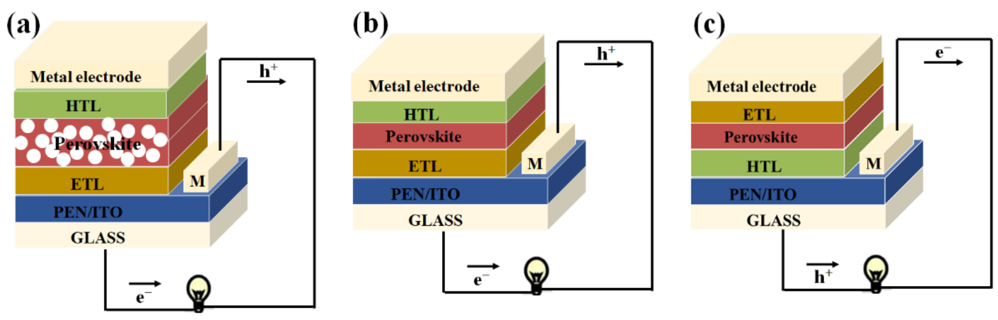
2.1. Architecture of Inverted PSCs

Since PSCs originated from dye−sensitized solar cells (DSSCs), architecture and working principle for devices are similar to those of DSSCs. As shown in Figure 2, the architecture of devices could be categorized into the upright architectures (n−i−p) and the inverted architectures (p−i−n). Moreover, the upright architectures (n−i−p) could be further classified into mesoporous structures and planar structures. Architecture of inverted PSCs consists of transparent conducting oxide (TCO), HTL, an absorption film, ETL and the metal back electrode as counter electrode, which is similar to the architecture of traditional upright PSCs. Normally, the HTL contains conductive polymers and inorganic semiconductor materials. The materials for ETL show less selectivity, mainly the fullerene and fullerene derivatives. The selection of ETL and HTL is based on the accessibility of the alignment of energy structure and preparation process.

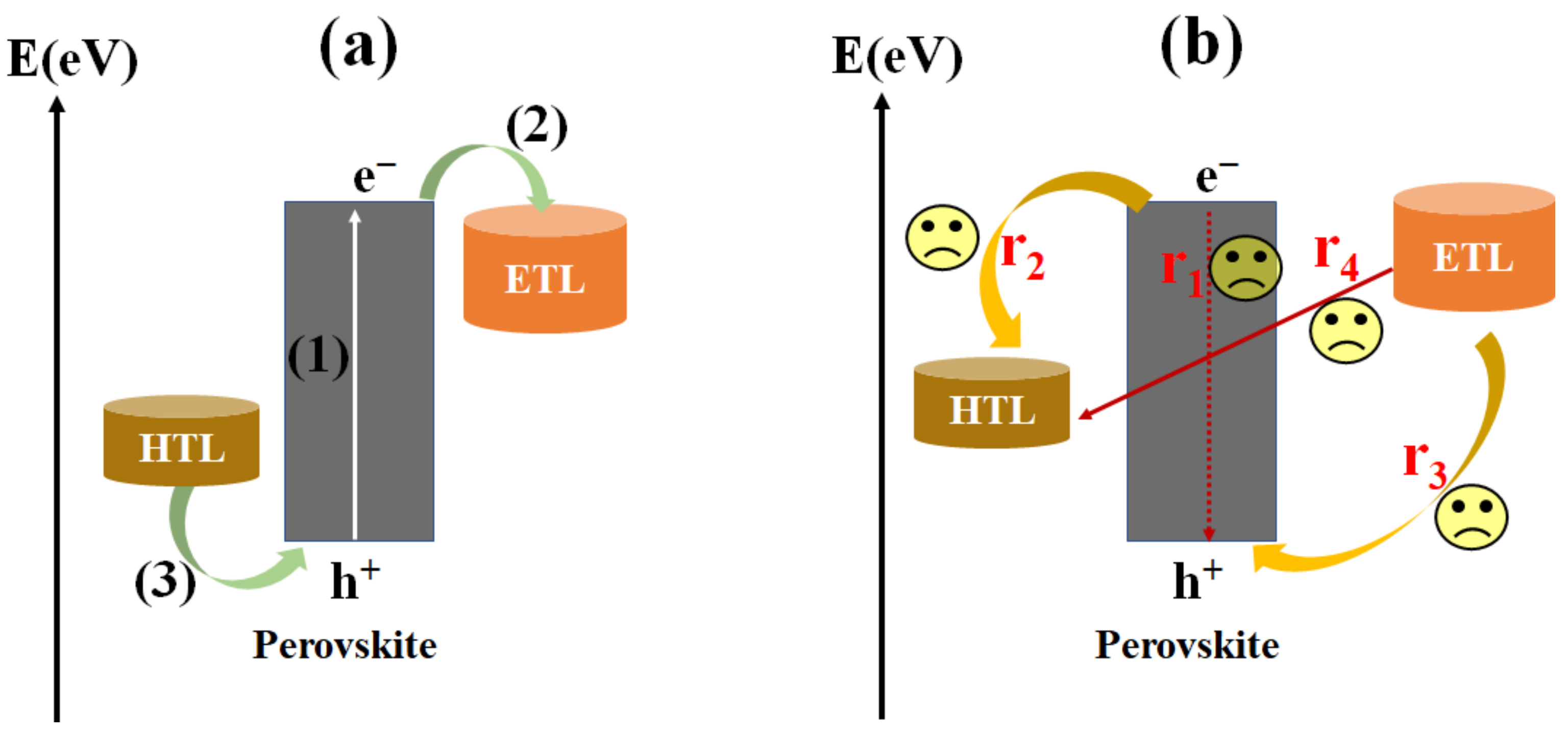
2.2. Working Principle of Inverted PSCs

The working principle of inverted PSCs can be expressed as follows [39,40,41]: (1) The perovskite absorber layer absorbs photons in light and creates electron–hole pairs under the excitation of light with enough energy, and then separates free carriers. The perovskite absorber layer, with a narrower bandgap, can absorb more sunlight and produce a higher photocurrent. However, this will give rise to lower open−circuit voltage due to the discrepancy of quasi−Fermi levels of carriers [39,40]. (2) The photoexcited holes are injected into the valence band (VB) of HTL and transferred to the TCO substrate due to the built−in electric fields, while the photoexcited electrons leap into the conduction band of ETL and transfer to the metal counter electrode for the reason given above. (3) The photoexcited electrons transfer to the cathode and the photoexcited holes are collected through the anode, which forms an electrical circuit. (4) However, the recombination process exists before hole injection to the HTL and electron injection to the ETL. As shown in Figure 3, before electron injection to the ETL, electrons in the absorber layer can recombine directly with holes in the absorption layer (r1) and with holes in the HTL (r2). In addition, the electrons in the ETL can react with holes in the absorption layer (r3), followed by recombination with holes in the HTL (r4).

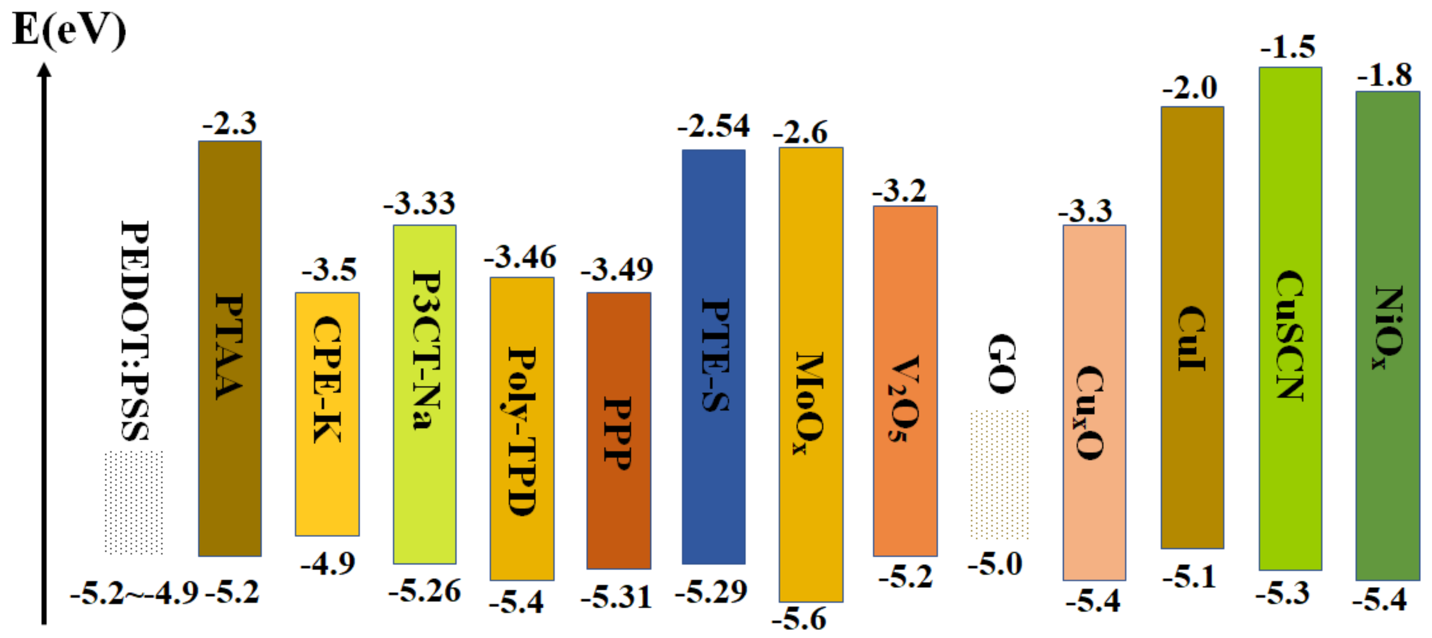
3. Hole−Transport Layer (HTL)

In order to accelerate the extraction of photoexcited holes in the absorption layer and reduce the energy loss, the HTL is introduced on the surface of TCO substrate in the inverted PSCs. The ideal HTL must fulfill the following requirements [41,42,43]: (1) Matched energy level. The highest occupied molecular orbital (HOMO) levels of HTL should be close to the VB of perovskite absorber layer. (2) High hole mobility. The high hole mobility favors the efficient transportation of photoexcited holes from the absorption layer to TCO substrate. (3) Good transmittance. Considering that the sunlight should get through the HTL before being absorbed by perovskite film, reduction of light loss can maximize the absorption and utilization of light. (4) Good film uniformity. The uniform film is beneficial to the generation of the absorption layer, with excellent crystallinity on the HTL. (5) Solution processability. Solution methods should not only simplify the preparation processes, but also be suitable for the commercialization of inverted PSCs in the future. For inverted PSCs, the types of HTL can be divided into conductive−polymer HTL, organic small−molecule HTL and inorganic−semiconductor HTL according to the property of materials. Figure 4 illustrates energy levels of different HTLs in inverted PSCs, including conductive−polymer materials (e.g., polytriarylamine (PTAA)), organic small−molecule materials and inorganic p−type semiconductor materials (e.g., NiOx and CuI) [44,45].

3.1. Conductive Polymers Materials

3.1.1. Poly(3,4−Ethylenedioxythiophene):Poly(Styrenesulfonate) (PEDOT:PSS)

Conductive−polymer materials have turned out to be a type of important p−type semiconductor material and have been used in various categories of thin film photovoltaic devices, such as organic solar cells devices, DSSCs, PSCs and so on. PEDOT:PSS has been extensively explored as HTL for inverted devices because of its excellent electron conductivity, high transmittance, the matched energy level and low temperature annealing process. Thus, great effort has been made to study its application in inverted PSCs. Performances of several representative inverted PSCs on the basis of pure PEDOT:PSS are shown in Table 1 [30,37,46,47,48,49]. In 2013, PEDOT:PSS was first used as hole transport materials in the inverted PSCs by Jeng et al., the efficiency of 3.9% was obtained [30]. However, the PEDOT:PSS−based inverted PSC suffered a poor Voc (0.88 ~ 0.95 V). In order to solve this issue, the pH value of PEDOT:PSS was controlled using imidazole [46,47,48]. Therefore, an improved efficiency of 15.7% with the Voc of 1.06 V was acquired for Wang et al., and an efficiency of 14.25% with the Voc of 0.994 V was acquired for Yi et al. Furthermore, stability of devices for long periods was enhanced due to the change in pH of PEDOT:PSS. Subsequently, Hu et al. prepared a PEDOT:PSS monolayers by using the water rinsing process on the ITO conductive substrate. A directional electric field from PEDOT with a positive charge to PSS with a negative charge was induced due to the Coulomb interaction of PEDOT and PSS, which can boost extraction of photoexcited holes. Furthermore, the PCE of 18.0% was yielded due to the enlarged Voc and fill factor (FF) [49]. Heo et al. prepared the inverted PSC with the PCE of 18.1% by depositing compact pinhole−free MAPbI3 perovskite film on the HTL by the spin−coating process, which was the highest PCE as ever reported with regards to pure PEDOT:PSS−based inverted PSCs until now [37].
Although the pure PEDOT:PSS shows good potential application for photoelectric properties of the inverted PSCs, there are some disadvantages that need to be overcome. First, the Fermi level of pure PEDOT:PSS mismatches with the energy levels of the absorption layer, which leads to the inefficient extraction of photoexcited holes and the low Voc. In addition, the hygroscopic property and acidity of PEDOT:PSS film will affect PSCs for long periods of stability. Numerous strategies, including doping PEDOT:PSS [50,51,52,53,54,55,56,57,58,59,60,61,62,63,64], modified PEDOT:PSS [32,65,66,67,68,69,70,71,72,73,74], interface engineering [75,76,77,78,79,80] and composite hole transport materials [81,82,83,84,85,86,87,88] have been developed to solve these issues.
(1)
Doping PEDOT:PSS
Doping of PEDOT:PSS has been widely employed to improve performance of photovoltaic devices. With regards to the inverted PSCs, the method of doping PEDOT:PSS was also studied to enhance properties of solar cells. Table 2 [50,51,52,53,54,55,56,57,58,59,60,61,62,64] shows the properties of several representative inverted PSCs on the basis of doping PEDOT:PSS with different substances. Doping could be applied to regulate the energy structure of HTL for inverted devices to enhance the hole transport performance of PEDOT:PSS and Voc [50,51,52,53,54,55,56,57]. For example, in 2018, Tang et al. tuned the work function of PEDOT:PSS from −5.02 eV to −5.19 eV by doping the HTL with the perfluorinated ionomer (PFI), and the optimal PCE of 15.85% was obtained [53]. Liu et al. doped rubidium chloride (RbCl) into PEDOT:PSS to elevate the properties of HTL [54]. By controlling the content of RbCl, it could enhance the work function of HTL, electrical conductivity and hole transport capability, which could simultaneously decrease the phase disengagement of PEDOT:PSS and enlarge the grain size, leading to an increased efficiency of 18.3%. In 2019, Jiang et al. enhanced the separation of photoexcited charge and hole transportation through doping PEDOT:PSS with CsI [55]. As a result, the PCE beyond 20% and a better Voc of 1.084 V were received for inverted PSC based on CsI−doped PEDOT:PSS. Meanwhile, doping PEDOT:PSS can improve morphology of the absorption layer [56,57,58]. For example, doping CuSCN into PEDOT:PSS not only led to the improvement of charge extraction efficiency, but also resulted in the rough surface topography of HTL. This induced the enlarged of perovskite crystalline sizes and the enhanced PCE [57].
Organic doping or p−type doping can also help to promote the electrical conductivity of PEDOT:PSS, including RuCl doped [54], Ag nano−particles doped [59], polyethylene oxide (PEO) doped [60], 2,3,5,6−tetrafluoro−7,7,8,8−tetracyanoquinodimethane (F4−TCNQ) doped [61], NaCl doped [62] and so on. In 2016, Hong et al. used the PEO−doped PEDOT:PSS as HTL to construct the inverted PSCs [60]. Doping CuSCN into PEDOT:PSS induced the improvement of its conductivity, which resulted in the effective transfer of photoexcited charge and the enhanced Jsc. Based on the investigation by Liu et al., it is regarded that doping F4−TCNQ into PEDOT:PSS can effectively tune electrical performance and HOMO level of PEDOT:PSS film [61]. As a result, the composite film revealed the improved electrical conductivity and beneficial energy level alignment, and the increased photoelectric performance (including Jsc, Voc, FF and PCE) was observed for inverted PSCs. Doping HTL with certain amount of NaCl could not merely contribute to enhancing the electrical conductivity of PEDOT:PSS, but help to induce the crystal orientation of perovskite layer along the (001) crystal plane on the film of HTL [62]. Recent studies suggest that the moisture stability and long−term stability can be enhanced through PEDOT:PSS [54,63,64]. In 2020, Xu et al. constructed the gradient heterojunction (GHJ) based on PEDOT:PSS/PEDOT:PSS−VOx by doping the content of VOx into PEDOT:PSS, resulting in the improvement of charge extraction and PCE [64]. Moreover, the GHJ−based PSC exhibited outstanding long periods of stability, which remained over 80% or 70% of the original efficiency under illumination in nitrogen atmosphere for 750 h or in the air for 175 h.
(2)
Modified PEDOT:PSS
In addition to the strategy of doping PEDOT:PSS, modification has been proved to be beneficial to solve problems of the inferior Voc and long−term stability. Performances of several representative inverted devices based on modified PEDOT:PSS are displayed in Table 3 [32,65,66,67,68,69,70,71,72,73,74]. Properties of PEDOT:PSS could be treated through solution processing [65,66,67,68]. PEDOT:PSS modified by dimethylformamide (DMF) solvent, Dimethyl sulfoxide (DMSO) solvent and the DMF solution of MAI was first reported by Xia et al., which led to the better electrical conductivity and superior surface of HTL [65]. As a result, it increased the Jsc while lowering FF and PCE of the inverted PSCs. Afterwards, researchers treated the PEDOT:PSS with these solutions by different approaches [32,66,67]. Chen et al. reported that PEDOT:PSS was rinsed with DMF to balance the carrier transport [32]. As a result, the charge transfer of devices was accelerated and balanced, which gave rise to the restraint of charge recombination at perovskite/selective contact interface and an improvement of PCE with 18.72%. Huang et al. modified PEDOT:PSS with certain percentage of DMSO, resulting in the PSC with a high light harvesting, and enhancing charge extraction and long periods of stability [67]. Apart from the common organic solvents, the use of 1−Ethyl−3−methylimidazolium chloride (EMIC) ionic liquids to promote the properties of PEDOT:PSS was reported firstly by Zhou et al. [68]. The treated PEDOT:PSS caused the excellent electrical conductivity, desirable surface morphology and lower work function for HTL, thereby obtaining the inverted PSCs with an increased efficiency.
On the other hand, performances of inverted devices could be promoted by modifying the chemical structure of HTL [69,70,71,72]. For example, in 2017, Huang et al. firstly applied dopamine (DA) to modify PEDOT:PSS to exploit a novel dopamine−copolymerized film [69]. As a consequence, it decreased the acidity of film, and improved the stability and PCE. Then, they further investigated the DA semiquinone radical treated PEDOT:PSS (DA−PEDOT:PSS) film and influence of DA doping on electron donating capability of DA−PEDOT:PSS [70]. The results of studies suggested that the DA−PEDOT:PSS exhibited enhanced charge extraction capability and work function, and the fabricated devices possessed improved Voc and an impressive PCE of 18.5% with high stability. Hydrogen peroxide (H2O2) can also be used to oxidize PEDOT:PSS monolayer to elevate the charge transmission performance for absorption layer to electrode and limit in−plane change transport [71]. As a consequence, the inverted devices based on the oxidized PEDOT:PSS monolayer yielded an enhanced FF of 0.82 and a PCE of 18.8%. In addition, hydroxymethyl (MeOH) can be added as a functional group to modify ethylenedioxythiophene (EDOT) [72]. Therefore, the work function of modified HTL was improved, and the energy level alignment, electrical conductivity and surface topography of PEDOT−MeOH:PSS were enhanced. Recent reports have discovered that the properties of PEDOT:PSS could be modified by using urea and sodium benzenesulfonate (SBS) to tune its morphology and work function [73,74], resulting in an excellent surface morphology and suitable energy level arrangement with the absorption layer, and better crystallinity of the absorption film.
(3)
Interface engineering
Apart from the modification, intercalation of interlayer film into the HTL can enhance the performance of inverted PSCs by interface engineering. Table 4 [75,76,77,78,79,80] shows the performances of several representative inverted PSCs on the basis of interfacial modification of the interlayer. First of all, the perovskite film will be in contact with the interlayer directly after the interlayer deposits on the PEDOT:PSS film, this will efficiently inhibit electron leak to restrain the charge recombination because of the high level of the lowest unoccupied molecular orbital (LUMO) about the interlayer. Jhuo et al. have employed the cross−linked organics N,N′−BIS(4−(6−((3−ethyloxetan−3−y)methox)−hexyloxy)peny−N,N′−bis(4−methoxyphenyl)biphenyl−4,4′−diamin (QUPD) and N,N′−biS(4−(6−((3−ethyloxetan−3−y)methoxy))−hexylpenyl)−N,N′−diphenyl−4,4′−diamn (OTPD) interlayers as electron blocking layers at the interface of HTL and absorption [75]. The HOMO level of cross−linked interlayers does match with that of the absorption layer, and the LUMO energy level of cross−linked interlayer was higher than that of HTL, which is beneficial to the hole collection and electron blocking. Second, the application of the interface between HTL and absorption layer, which can tune the energy structure mismatch, such as polyethyleneglycol (PEG) interlayer and N,N′−Bis−(1−naphthalenyl)−N,N′−bis−phenyl−(1,1′−biphenyl)−4,4′−diamine (NPB) interlayer [76,77,78], and FF can be improved [77]. Third, the inserting of the interlayer can strengthen the contact interface between PEDOT:PSS and absorption film, and then modify morphology of perovskite film [78,79]. Gu et al. applied 3−aminopropanoic acid as a monolayer with self−assembly (C3−SAM) on HTL [79]. As a consequence, C3−SAM could remarkably enhance crystallinity and coverage of the absorption layer. At last, interlayer at the HTL/absorption layer interface can inhibit the corrosion of perovskite precursors on substrates and the decomposition of absorption film due to the hygroscopic property and acidity of HTL, which resulted in an improvement of the stability for solar cells [80]. Luo et al. fabricated a graphene−oxide (GO) coating layer on the HTL [80]. The GO interlayer has been effectively enhanced the morphology of absorption layer and restrained decomposition of absorption layer. As a consequence, the PSC showed a PCE of 15.34% and the stability was obviously enhanced with efficiency remaining at 83.5% of the original value when exposed to the air up to 39 days.
(4)
Composite HTL materials
The photoelectric properties of PEDOT:PSS−based inverted devices could also be strengthened with modifying another p−type hole transport material. Through this process, the other hole transport material can make up the shortcoming of PEDOT:PSS layer and contribute to improvement performance of devices: (1) Adjust the energy level arrangement in the architecture. (2) Promote the film quality of perovskite layer. (3) Accelerate the carriers transport at the HTL/absorption layer. (4) Advance the stability of devices. (5) Enhance the electron−blocking capacity. Performances of several representative inverted devices on the basis of the composite film are shown in Table 5 [81,82,83,84,85,86,87,88]. For example, V2O5 was used as the HTL to tune the energy level alignment in the inverted PSCs, which led to the increase of the work function (from 5.1 to 5.4 eV) and a boosted efficiency of 17.5% [81]. Nickel phthalocyanine (NiPcS4) was incorporated into HTL, resulting in the increase of perovskite crystallinity, charge transfer at HTL/absorption layer interface, and the stability in the air [82]. These factors led to efficiency up to 18.9%. Yoon et al. fabricated a hybrid HTL that consists of the single−walled carbon nanotubes (CNTs) and PEDOT:PSS for inverted PSCs [83]. The hybrid HTL exhibited a superior quality film and the enhanced electron−blocking properties, which increased the PCE from 13.2% to 16.0%. Li et al. developed a hybrid HTL by incorporating the oxidized carbon nanorods (OCNRs) into the HTL [84]. The hybrid HTL could tune energy level alignment between HTL and absorption layer, resulting in an enhanced efficiency of 19.02%. It is worth noting that most of the composite hole transport materials are based on PEDOT:PSS for the inverted PSCs so far.

3.1.2. Poly(Bis(4−Phenyl)(2,4,6−Trimethylphenyl)Amine) (PTAA)

PTAA is regarded as another typical of conductive polymers HTM. These inverted PSCs which recently reported the highest efficiency are on the basis of PTAA. Table 6 [34,89,90,91,92,93,94,95,96,97,98,99,100,101,102] shows the performances of several representative inverted PSCs devices on the basis of the different PTAA HTL structures. On one hand, PTAA is the typical π−conjugated organic polymer material and its non−planar molecular structure is amorphous. This will lead to the dense and uniform film and excellent isotropic hole transport performance. On the other hand, the inferior Voc of inverted PSCs is mainly because of nonradiative recombination. Furthermore there is no microstructural ordering during annealing for PTAA. This will reduce the nonradiative recombination in the interface. In addition, hydrophobic property of PTAA would favor the stability of the devices. However, some articles showed that the UV light can cause the PTAA degradation, which can interfere with the charge transport, as well as increased defect population upon prolonged UV exposure. So, some actions should be taken to improve its resilience, such as doping materials or adding a layer [103].
As early as 2015, Bi et al. systematically researched hydrophobic property of wetting and non−wetting polymer HTLs, such as polyvinyl alcohol (PVA), PEDOT:PSS and PTAA, the growth mechanism of MAPbI3 perovskite crystals on the HTL substrates [89]. The results indicated that MAPbI3 crystals on PTAA have significantly larger grains, higher crystallinity and fewer grain boundaries compared with that on the wetting HTL substrates. This will reduce the crystal defects and the nonradiative recombination in the absorption layer, resulting in the outstanding efficiency of 18.1% for PSC on the basis of the PTAA. Subsequently, in 2017, Serpetzoglou et al. targeted researched the hydrophilic PEDOT:PSS and the hydrophobic PTAA polymer HTLs, along with the corresponding inverted PSCs. The device on the basis of PTAA exhibited the better photoelectric performance with the PCE of 15.67%, but the device on the basis of PEDOT:PSS obtained the efficiency of 12.6% [90]. This is mainly due to the decrease of HTL surface roughness, and the hydrophobic performance of HTLs only explained a little about the difference in the photoelectric performance. By 2018, Luo et al. groundbreaking had reported that the nonradiative recombination of the inverted devices was effectively reduced by using a solution−processed secondary growth technique with bromide guanidine solution, leading to the highest PCE of 21.5% ever up to that time for PTAA/perovskite/PCBM/C60/BCP/Cu device [34].
However, PTAA as a kind of polymer semiconductor is now faced with the problem of poor electrical conductivity. Doping is an efficiently strategy to enhance properties of PTAA. Wang et al. reduced device series resistance by doping F4−TCNQ in PTAA, resulting in an improvement of FF and Voc without sacrificing short circuit current [91]. However, the F4−TCNQ had the problems of poor solubility and high cost. Recently, Liu et al. have introduced a NPB film into PTAA to strengthen the wettability of PTAA and promote the surface topography of the absorption layer [92]. Consequently, the optimal PSC exhibited excellent photoelectric performance and obtained a PCE of 20.15%.
The poor electrical conductivity of PTAA exists not only at the ITO/PTAA interface, but also between the PTAA and perovskite film. Therefore, modification is also an efficient strategy to promote the performance of PTAA [93,94,95,96,97,98]. Reduced graphene oxide (rGO) is also widely doped into HTL by researchers [104]. Zhou et al. employed the stability of reduced graphene oxide (rGO) to construct the ITO/r−GO/PTAA hole−transport bilayer, leading to a decrease of defects in the absorption layer and an increase of PCE with 17.2% for the rigid inverted PSCs [94]. It is well−known that the monomolecular HTL often exhibits superior surface and electronic properties compared with the regular HTL. However, the study showed that the work function and conductivity of monomolecular HTL were decreased [97]. To solve this problem, Chen et al. introduced the 2,3,5,6−tetrafluoro−7,7,8,8−tetracyanoquinodimethane (F4−TCNQ) as the interlayer between PTAA and perovskite film, resulting to an improvement performance of device [97]. Polyelectrolyte is often used as the typical material for interfacial modification to enhance performance. Jung et al. used a series of anionic conjugated polyelectrolytes (CPEs) as the interlayer between PTAA and absorption layer [98]. As a result, the wetting and morphology of the absorption layer were enhanced because of the improved wettability of perovskite on the PTAA, so a large−area solar cell obtained a stable PCE of 18.38%.
In addition, one of the most frequently used methods is interface engineering for improving the properties of HTL, especially for the surface properties of HTL [99,100,101,102]. Though the hydrophobic property of PTAA can promote the stability of the inverted devices, PTAA makes the precursor of absorption layer difficult to cover on the PTAA substrate due to its large surface energy, and many researchers have used the means of interface engineering to improve the surface activity of PTAA toward perovskites [99,100,101,102]. In 2018, oxygen plasma processing is employed to modify the hydrophobicity of HTL by Zhang et al. [99]. The oxygen plasma treatment not merely decreased the surface energy and enhanced work function of HTL but increased electrical conductivity of HTL. As a result of the treatment, the efficiency of charge extraction was enhanced, and the inverted PSCs with oxygen plasma treated PTAA acquired a PCE of 19.0%. The hydrophobicity of PTAA can also be improved via solvent treatment process. In 2020, Li et al. modified the surface of PTAA by toluene during solution processing, resulting in the enhancement of wettability of PTAA and the improvement of morphology [100]. Apart from that, it is conducive to the holes extracted from absorption film to HTL, and the ohm contact between the PTAA and perovskite film has been enhanced. As a consequence, inverted PSCs illustrated an excellent efficiency of 19.13%. Recently, Xu et al. have textured the PTAA by demixing of the mixed polymer solution with PTAA and polystyrene (PS), and obtained a textured PTAA/perovskite interface [102]. By adopting an antireflection coating on ITO substrate, the device based on the textured PTAA exhibited a superior PCE with 21.6%.

3.1.3. Conjugated Polyelectrolyte (CPE)

As the most commonly used material, PEDOT:PSS has unavoidable shortcomings, such as acidity and hygroscopicity. This leads to the poor stability and repeatability for the PSCs. However, CPE with pH−neutral and preparation at low temperature, as a new kind of HTL, avoiding the disadvantages of PEDOT:PSS successfully. More importantly, the energy level of CPE could be adjusted, which is beneficial to reduce interface contact resistance at active layer/electrode interface. In addition, functional group in the side chains of CPE can ensure good solubility in water and alcohol. Table 7 [105,106,107,108] shows the performances of several representative inverted PSCs on the basis of the different CPE HTL structures. In 2015, Choi et al. employed CPE with the decoration of functional group as the HTL to prepare a CPE−K film, which was used in PSCs for the first time [105]. Their devices with the CPE−K resulted in a maximum efficiency of 12.51% with elevated stability. CPE with the decoration of different inorganic ions has an effect on the self−doping capacity, conductivity and the adjustment of work function for HTL. Thus, many CPE based HTLs with the decoration of inorganic alkali metal ions [106,109,110], such as SO3K+, SO3Na+ and COONa+, have been developed since the first report. By contrast, CPE with organic cations has been applied in PSCs by researchers [107]. The results demonstrated that CPE with organic cations shows an excellent wettability to the absorption film, leading to an excellent efficiency with 19.76% [106]. After that, in 2020, Zhang et al. incorporated K+ into the CPE (TB(K)) to enhance the defect−passivation properties [108]. The result is that devices based on TB(K) displayed a superior photoelectric property with an efficiency of 20.1% due to the favorable inhibition of defect state and collection efficiency of photoexcited holes for TB(K).

3.1.4. Polyelectrolyte

The work function of PEDOT:PSS mismatches with energy levels of absorption layer according to previous reports, which leads to the energy loss at HTL/absorption layer interface and lower Voc of solar cells [49,50,51,52,53,54,55,56]. In order to overcome this shortcoming, polyelectrolyte was developed as a substitute of PEDOT:PSS considering its excellent performance in the fields of organic light emitting diodes (OLEDs) and organic solar cells (OSCs). The introduction of polyelectrolyte can lead to the forming of dipole at the ITO/polyelectrolyte interface and regulate work function of ITO, resulting in an improvement of carrier extraction and photoelectric properties. Table 8 [111,112,113,114] shows the performances of several representative inverted PSCs devices on the basis of the polyelectrolyte structures. In 2015, Li et al. used water soluble polyelectrolytes (P3CT−Na) as HTL in PSCs to facilitate the performance for the first time, which resulted in an excellent performance with PCE of 16.6% due to the desirable match of energy structure and favorable crystal of perovskite film [111]. To modify surface wettability of P3CT−K, doping of graphdiyne in P3CT−K was carried by Jiu et al. in PSCs, resulting in an improvement of hole collection efficiency and a decrease of charge recombination [113]. Therefore, Jiu et al. further employed the small molecule ethanediamine to construct a novel polyelectrolyte (P3CT−ED). As a result, application of P3CT−ED can significantly improve the hole transport of P3CT−ED and the crystallinity of perovskite film, as well as reduce surface defects.

3.1.5. Poly[N,N′−Bis(4−Butylphenyl)−N,N′−Bis(Phenyl)Benzidine] (Poly−TPD)

As the typical non−wetting hole transport materials, Poly−TPD possesses the higher LUMO energy level in comparison to PEDOT:PSS material, which give rise to an efficient collection of photoexcited holes and separation efficiency of photoexcited charge, as well as facilitating the crystal growth of perovskite materials. Thus, the large−sized perovskite crystalline and few lattice defects of perovskite films were obtained for PSCs based on Poly−TPD HTL by Zhao et al. [115]. Table 9 [115,116,117,118,119] shows the performances of several representative inverted PSCs devices based on the Poly−TPD HTL structures. Xu et al. adopted ultraviolet−ozone modification method to tune the surface wettability of Poly−TPD to improve the absorption layer with desirable crystallite dimension and favorable coverage, and a highest PCE of 18.19% was acquired [116]. Interface modification is an effective method of improving the interface contact and reducing the defect states between the HTL and the perovskite films [117,119]. You et al. introduced an insulating layer of Al2O3 nanoparticles to decrease the surface energy of hole transport materials, which resulted in perfect optoelectronic properties of HTL and the full Voc [117]. Li et al. used the conjugated polyelectrolyte (PFN−I) to enhance the interface contact and reduce the defects at HTL/absorption layer interface and perovskite/ETL interface simultaneously, leading to the enhancement photoelectric properties and stability of PSCs devices [119]. An outstanding efficiency of 20.47% and over 80% of the original efficiency were observed for the prepared devices with 800 h under humid conditions, with 35–55% at room temperature.

3.1.6. Other Conductive Polymer Materials

High cost is a problem which cannot be ignored for the most popular conductive polymers HTL. For example, PEDOT:PSS and PTAA. With that in mind, other conductive polymers are also used as the HTL of inverted PSCs, such as polythiophene and poly(p−phenylene) (PPP) [120,121]. Table 10 [120,121,122,123,124] shows the performance of several representative inverted PSCs on the basis of other conductive polymers HTL. Yan et al. deposited the prepared the polythiophene on the ITO surface as the HTL via electrochemical polymerization, and the inverted PSC based on polythiophene showed a promising efficiency of 15.4% [120]. They further prepared a sequence of conductive polymers, such as PPP and polythiophene (PT), as the HTL using electrochemical polymerization [121]. The constructed devices based on PPP exhibited an outstanding Voc with 1.05 V and an efficiency of 16.5% due to its work function of −5.31 eV. Wang et al. adopted conjugated polymer poly(9−vinylcarbazole) (PVK) as the HTL, and found that PVK based devices had better stability in contrast to PEDOT:PSS based devices [122]. In addition, a superior charge recombination resistance of PSCs was obtained due to the fact that perovskite film has preferable crystal properties and fewer PbI2 surplus. Liu et al. prepared two new types of nonlinear π−conjugation molecules as the HTL, which were Y−shaped (XSln847) and X−shaped (XSln1453) [123]. Compared to the X−shaped molecule, a Y−shaped molecule has superior charge transfer and reduced charge recombination due to the fact that XSln847 molecule forms a compact stacking arrangement of molecules through short contacts between molecules to achieve a nest−layer in molecules. As a consequence, an efficiency of 17.16% was acquired with XSln847 based PSC.
In addition to them, the method of dopants is considered to be an effective strategy to settle the defects of hole mobility and charge recombination for other conductive polymers materials. Therefore, Shao et al. developed a low−cost in situ electropolymerized polyamines (poly−1) as HTL for inverted PSCs [124]. The results of research suggested that the undoped poly−1 has superior hole collection ability and carriers transport properties, as well as strong hydrophobicity. As a result, the inverted PSCs with the optimal undoped poly−1 exhibit excellent long−term stability and a greatest efficiency of 16.5% compared with that for undoped PTAA.

3.2. Organic Small−Molecule Materials

Compared to the conductive polymer materials with high cost and complex synthesis process, small−molecule hole−transport materials not only have the advantages of simple synthesis, low cost and easy purification, but also can optimize the chemical structure and photoelectric performance by molecular engineering, which has gradually attracted the interest of researchers [125]. With the efforts of researchers, the efficiency of inverted PSCs based on organic small−molecule materials is increasing, and it tends towards catching up with PTAA. Table 11 [126,127,128,129,130,131,132,133,134,135,136,137,138] shows the performances of several representative inverted PSCs based on organic small−molecule HTLs. Instead of PEDOT:PSS, Li et al. employed two kinds of original micro−molecule organics 4,4′−bis(4−(di−p−toyl)aminostyryl)biphenyl (TPASBP) and 1,4′−bis(4−(di−p−toyl)aminostyryl)benzene (TPASB) as the HTL in inverted devices [126]. In comparison with PEDOT:PSS, TPASBP and TPASB with linear π−conjugated structure showed efficient hole transport properties, and the perovskite film on them presented large crystals and reduced grain boundaries. Hence, an efficiency of 17.4% and 17.6% was obtained for inverted devices based on TPASBP and TPASB HTLs. Yang et al. used the micro−molecule organics 4,4′−cyclohexylidenebis[N,N−bis(4−methylphenyl) benzenamine] (TAPC) as HTL in inverted PSCs [127]. Smooth, uniform, and hydrophobic TAPC with π−conjugated structure were achieved with the optimization of solution concentration and annealing temperature, leading to an outstanding efficiency of 18.8%. Zhang et al. prepared and adopted four diphenylamine derivatives with a fluorene core as HTL in inverted PSCs [128]. The insoluble 3D networks can be formed for the synthesized HTL with vinyl crosslinking via a suitable annealing temperature, leading to a low solvent resistance for preparation and a better stability. Hence, the device with the optimized HTL illustrated the prominent efficiency of 18.7% with the highest Voc of 1.15 V. Li et al. used the micro−molecule organics (NPB) without dopants as HTL in MAPbI3 based inverted devices, leading to a prominent absorption layer with better crystallization properties, as well as a best PCE of 19.96% [129]. In 2019, Cao et al. showed an organic micro−molecule with spiro−based dopant−free (DFH) as HTL, which has a suitably positioned HOMO level for effective charge transfer from perovskite and the functional groups to adjust the conductivity and hole mobility [130]. As a result, the charge recombination was inhibited and an outstanding efficiency of 20.6% was achieved. In addition, DFH has an obvious advantage in price compared with other commonly used materials. Soon after, Wang et al. succeeded in increasing the efficiency of the inverted PSCs based small−molecule HTL to over 21% [131]. Not only the reported MPA−BTI and MPA−BTTI molecules have excellent photoelectric properties, but also the Lewis base groups in the molecules could inhibit defect states of absorption layer, which will give rise to enhanced performance of devices. With development of all−organic PSCs, Jiang et al. fabricated a novel 3D micro−molecule organics (TPE−S) as HTL in inverted all−organic CsPbI2Br PSCs, which exhibited a greatest efficiency of 15.4% because of the enhanced photoelectric properties, superior interfacial energetics, matched energy band structures and reduced charge recombination [132]. Furthermore the inverted hybrid PSCs obtained up to a PCE of 21.0%. Therefore, the reasonable design of molecular structure can achieve effective preparation for inverted devices on the basis of small molecules.

3.3. Inorganic Semiconductor Materials

3.3.1. NiOx

NiOx is a typical P−type inorganic material with a wide bandgap, usually representing a mixture of nickel (IV) and nickel (III) oxide (NiOx), which is the focus of current researches among P−type inorganic semiconductors. The researches show that NiOx has high transmissivity, efficient charge extraction capability, and the matched energy level with perovskite [139,140,141]. Table 12 [140,141,142,143,144,145] shows the performances of several representative inverted PSCs based on NiOx. Docampo et al. adopted NiOx as HTL in the inverted PSCs through calcination of nickel acetate tetrahydrate and monoethanolamine on a conductive substrate for the first time [139]. However, the efficiency of constructed device is less than 1%. This can be attributed to that the NiOx in inverted PSCs is difficult to support an enough thick perovskite absorption layer, leading to a relatively inferior covering surface of absorption layer on NiOx substrate. Thus, the enhancement of anchoring capability for NiOx is the key to improving the NiOx based devices. For this matter, Zhu et al. synthesized the NiOx layer with high transparency as HTL via a sol−gel process [140]. The prepared NiOx nanocrystals have a corrugated surface and well contacted with FTO substrates, which could support a sufficiently thick perovskite (300 nm) film. As a result, an excellent efficiency of 9.11% was acquired for the inverted devices on the basis of NiOx nanocrystals HTL. However, the photoelectric performances of inverted PSCs on the basis of the NiOx are still far behind that of inverted PSCs based on polymers materials and PSCs based on n−i−p structure. For this reason, in 2015, Park et al. improved the efficiency to as high as 17.3% with the FF value of 0.813 by preparing a well−ordered nanostructured NiOx with a pulsed laser deposition method, which was the highest efficiency achieved at that time for the inverted PSCs based on P−type inorganic materials [141]. However, the preparation method with pulsed laser deposition method is inapplicable to the fabrication of large−scale devices. Therefore, Yin et al. adopted a small nanocrystal NiOx film with cubic structure as HTL via a solution process with optimized concentration [142]. The obtained NiOx film, with high conduction band, exhibited a superior electron blocking property, leading to a cell with less hysteresis, better air storage stability and 14.42% PCE. Islam et al. employed the sputter−deposited method to prepare the NiOx film as HTL [143]. With optimized preparation condition of NiOx, the inverted devices based on the polycrystalline NiOx film showed a better stability and a high PCE of 15.2%. Tang et al. prepared the NiOx film with superior transmittance via sol−gel method, and its matched energy level and excellent optical transmittance led to a high PCE of 18.15% for the inverted devices [144]. Mali et al. prepared P−type nanoporous NiOx (np−NiOx) film via a coprecipitation process, and an excellent efficiency of 19.1% was acquired for the inverted devices on the basis of np−NiOx [145]. More importantly, more than 80% initial efficiency was restrained with 160 days at the air environment. Therefore, the preparation method played an important part in the properties of nickel oxide and photovoltaic devices, application of appropriate methods and optimization of preparation conditions can fabricate photovoltaic devices with excellent efficiency.
(1)
Doping NiOx
Element doping is one of the most efficient ways to improve photoelectric performance of NiOx HTLs. Doping elements are usually alkali metals (e.g., Li+, K+, Cs4+), alkaline earth metals (e.g., Mg2+), transition metals (e.g., Y3+, Cu2+, Ag+) and micro−molecule organics (F6TCNNQ), as is shown in Table 13 [146,147,148,149,150,151,152]. The advantages of doped NiOx film are as follows: (1) Higher conductivity can effectively accelerate the extraction and transfer of photoexcited charges at NiOx/perovskite interface and reduce the series resistance of devices; (2) The work function of NiOx film is closer to top of the VB of perovskite film, resulting to the higher hole mobility; (3) The transmittance of NiOx film is improved, and absorption layer on NiOx layer has better crystallinity and higher coverage.
Copper (Cu) was incorporated into the NiOx film as a dopant by Kim et al. [146]. Doping of copper ions could efficiently promote the electroconductivity of NiOx, which accelerates extraction of photoexcited holes at NiOx/perovskite interface and reduces the series resistance of PSCs. It turned out that the efficiency of copper (Cu)−doped NiOx (Cu:NiOx) based device was increased to 15.4%, as well as the Jsc and FF. In 2015, Chen et al. added lithium (Li+) and magnesium (Mg2+) to conduct heavily doped the NiOx film to promote photoelectric performance of NiOx. Strategy of lithium−magnesium (Li+ − Mg2+) doping NiOx film (Li0.05Mg0.15Ni0.8O) enhanced the extraction of photoexcited charge, and avoid the morphology of pinholes, as well as the local structural defects of PSCs for the large area devices [147]. In addition, Mg2+ doping compensates the band shift caused by Li+ doping into the lattice, leading to a high PCE of 18.3% and a large−area (˃1 cm2) device with 16.2%. Cesium (Cs2+) doped NiOx film (Cs:NiOx) was conducted to prepare the HTL in inverted PSCs devices by them in 2017 [148]. The introduction of Cs2+ ions improved the conductivity and work function of NiOx film, and finally realized a high PCE of 19.35%. In 2018, Wei et al. reported a novel inorganic HTL based on Ag+ doped NiOx (Ag:NiOx) [149]. Transmittance, work function, electroconductivity and hole mobility of NiOx film could be elevated by replacing Ni site with Ag+ (AgNi) and behaving as the acceptor in NiOx lattice. Absorption layer on Ag:NiOx HTL show superior crystals, preferable covering surface and smoother topography, leading to a PCE of 16.4%, consequently. Yttrium (Y) was incorporated into the NiOx film as a dopant via sol−gel method by Hu et al. [150]. The obtained Y:NiOx HTL exhibited high hole mobility and quality morphology of perovskite film, which promoted interface charge recombination and transfer, and achieved an efficiency of 16.31%. Chen et al. successfully introduced an organic small molecule (F6TCNNQ) into the preparation of NiOx film, which improved Fermi energy level of NiOx and reduced energy level offset between NiOx and absorption layer [151]. Consequently, the efficiency of CsFAMA based devices was raised to as high as 20.86%.
(2)
Interface modification
Interface modification is another efficient way to promote photoelectric properties of NiOx, which can avoid possible uneven doping and unmanageable disorders caused by element doping, as is shown in Table 14 [153,154,155,156,157]. A few years earlier, interfacial layer was employed to promote the deficiency of NiOx film in the inverted devices [153,154]. In 2015, Chen et al. prepared an ultra−thin NiOx film through spray pyrolysis method and introduced an inert mesoporous alumina (Al2O3) with high transmittance as the barrier layer, leading to a higher PCE of 13.5% [153]. However, the obtained photoelectric property of inverted devices is far behind that for other structures HTL. Considering the problem of serious interfacial recombination, Chen et al. employed a potassium chloride (KCl) interface modification to reduce the interfacial recombination [155]. The modification of KCl led to an enhancement of absorption film and decrease of defect/trap density, resulting in an obvious enhancement in the Voc from 1.07 eV to 1.15 eV. Lian et al. used an insulating film of PTAA film to improve the contact at NiOx/absorption film interface to decrease defects, which led to a better energy level arrangement, a deeper HOMO of NiOx/PTAA, less interface energy loss and a superior Voc as high as 1.19 eV [156]. In 2020, Ru et al. employed the contrivable molecules (F2HCNQ) to adjust the conductivity and energy level of NiOx film, resulting in a highest PCE of 22.13% with an FF of 82.8% [157]. Therefore, the designing of appropriate interface modification is an efficient method of acquiring excellent performance of inverted devices.

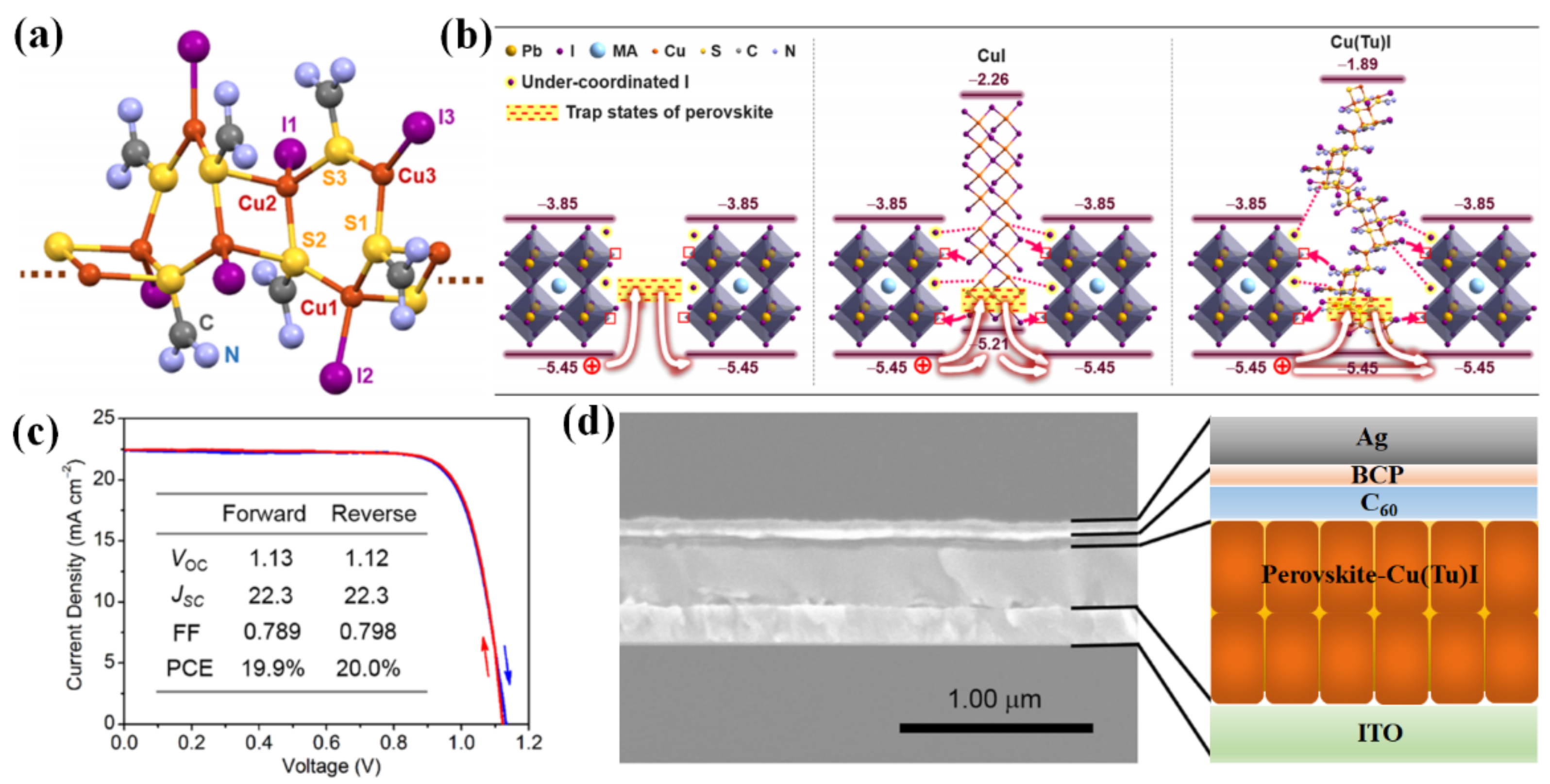
3.3.2. Cu−Based Materials (CuX)

Cu−based materials (CuX), as typical P−type materials, have high carrier mobility and carrier diffusion length. More importantly, the matched energy level of CuX HTLs can effectively prevent the leakage of photoexcited electrons and reduce the energy loss of perovskite solar cells, especially for copper thiocyanate (CuSCN) and copper iodide (CuI). Hence, several representative inverted devices on the basis of the Cu−based HTL structures were reported, as is shown in Table 15 [158,159,160,161,162,163,164,165,166,167,168,169]. In 2014, Subbiah et al. showed the electrodeposited CuSCN as HTL in inverted devices firstly, resulting in the PCE of 3.8% [158]. However, the obtained PCE is far behind that for the organic HTLs based devices. Ye et al. fabricated a high−quality absorption layer on the electrodeposited CuSCN film, which led to a smaller surface roughness of absorption layer and lower interface contact insistence at CuSCN/absorption film interface [159]. It turned out that the average PCE was promoted to 15.6% with the best efficiency of 16.6%. CuI, whose energy level structure was similar to CuSCN, is also used as HTL in inverted PSCs [160,161,162,163]. Chen and Sun et al. used a spin coating CuI as HTLs in inverted devices, leading to the high efficiency of 13.58% and 16.8% [160,161]. Wang et al. exposed the heat evaporated Cu layer to iodine steam to prepare a uniform CuI film, and used the CuI as the HTL of inverted devices, achieving an efficiency of 14.7% in CuI/MAPbI3/PCBM/Au structure [162]. In 2017, Ye et al. first inserted a original p−type Cu(thiourea)I (Cu(Tu)I) as trap state passivators (TSPs) into the absorption film for the inverted PSCs to decrease the trap states of absorption film, as is shown in Figure 5 [163]. The trap states of absorption layer were passivated through interaction of Cu(Tu)I and uncoordinated metal cations and halide anions on the surface of absorption film, and depletion width of p−i bulk heterojunctions was increased, which led to the acceleration of excited hole transfer, the reduction of charge recombination and a breakthrough certificated PCE of 19.9%.
P−type CuxO has a narrower bandgap (2.2 eV) and the work function of −5.4 eV in comparison to CuSCN and CuI. The CuxO crystal with small size is easy to get high quality film with uniform surface topography, which is conducive to the crystalline grow of perovskite film. Wu et el. prepared an ultrathin Cu2O thin films via thermal oxidation method and applied in the inverted devices with CuOx/MAPbI3/PCBM/Ag structure [164]. The photoelectric performance of devices is extremely vulnerable to thickness of Cu2O film, and an efficiency of 11% was acquired with the thickness of 5 nm Cu2O films through precisely optimizing the thickness of Cu2O layer due to the high hole mobility, matched energy structure with perovskite film and long lifespan of photoexcited charges. In 2017, Yu et al. prepared CuOx film as HTLs in inverted PSCs via a solution process, and the high quality of perovskite film was achieved based the CuOx film [165]. As a result, the hole extraction was improved and the stability of devices was enhanced, which lead to the high performance of device with a PCE of 17.43%. In addition to the above commonly used Cu−based materials, other Cu−based materials were also developed as HTLs in inverted devices, for instance CuS and Cu3PS4 [166,167]. Rao et al. firstly applied CuS nanoparticles as HTL in inverted PSCs using the solution processing, which can effectively improve the extraction of photoexcited holes and achieve a PCE of 16.2% with optimization [166]. Yin et al. firstly applied Cu3PS4 nano materials as a novel HTL for inverted devices, which was conducive to growth of absorption film on the Cu3PS4 HTL and leads to a maximum PCE of 18.17% with less hysteresis [167].
Compared with NiOx, Cu−based materials have a relatively narrow band gap (2~3 eV), which is beneficial to inhibit the recombination of photoexcited charge due to the reverse transport of photoexcited holes. However, the Cu−based materials have higher requirements on the quality, thickness and transparency of HTLs. Compared with other hole transport materials, Voc and FF are relatively low, which can be ascribed to low charge collection at HTLs/absorption layer interface and large series resistance at the interface. Hence, interface modification, the hole transport bilayer and ion doping can be used to improve the photoelectric properties of HTL. In 2018, Wang et al. incorporated the CuSCN into the CuI HTL by a solution process method, resulting in high quality HTLs with higher conductivity and an impressive PCE of 18.76% [168]. Javaid et al. employed a hole transport bilayer composed of PTAA and CuI in the inverted PSCs devices, which gave rise to a high grade absorption layer with larger crystals and a highest efficiency of 20.34% [169].

3.3.3. Other Inorganic Semiconductor Materials

In addition to NiOx and Cu−based materials, other inorganic semiconductor materials were used as the HTL for inverted devices, for instance V2O5, MoOx and CoOx, as is shown in Table 16 [170,171,172,173,174,175,176,177,178]. Graphene oxide (GO) with applicable work function (−4.9 eV) is used as a HTL of inverted PSCs, which can effectively improve the film quality of perovskite layer [170,171,172,173,174]. Wu et al. employed GO as a HTL in the inverted devices for the first time, resulting in high grade absorption layer and the PCE of 12.4% [170]. Yeo et al. demonstrated the reduced graphene oxide (RGO) as HTL through a solution and room−temperature process [171]. The inverted devices consisting of a structure of rGO/MAPbI3/PCBM/BCP/Ag exhibited an enhanced PCE of 10.8% with good reproducibility and desirable stability. Chen et al. employed oxo−functionalized (oxo−G1) as HTL in inverted devices by a solution process to solve the stability issues of PSCs [172]. As it turned out, oxo−G1−based inverted devices illustrated an obviously enhanced stability and an efficiency of 15.2% with the outstanding Voc of 1.1 V. Wang et al. treated GO with ammonia via a general strategy to prepare the HTL for the inverted devices, considering the acidic nature of GO [173]. Consequently, the devices fabricated on the basis of ammonia−treated GO (a−GO) obtained enhanced PCE of 14.14% and environmental stability. In 2021, Csatriotta et al. employed potassium−doped graphene oxide (GO−K) as the interlayer between the mesoporous TiO2 and the perovskite layer and used infrared annealing (IRA). The final PCE was 18.30%, and the hysteresis of the devices was significant reduced [179].
V2O5 has a narrow band gap (2.0 eV) and a low work function (−5.2 eV), which could gain the effective hole extraction junction with absorption film and has been investigated to replace the frequently used HTL in inverted PSCs [139,174,175,176]. Docampo et al. used V2O5 as the hole transport materials for inverted devices with the construction of V2O5/MAPbI3−xClx/PCBM/TiOx/Al, and the PCE was less than 1% [139]. Guo et al. fabricated V2O5 thin films through a solution process method and obtained device with PCE of 5.1%. After that, they fabricated thin V2O5/PEDOT nanoribbons via a cocoon−to−silk−fiber reeling process as HTL for inverted devices, resulting in a high PCE of 8.4% [175]. Duan et al. prepared a hole transport bilayer composed of V2O5 and P3CT−K as HTL in the inverted PSCs, which gave rise to the boosting efficiency of 19.7% [176]. Furthermore, bilayer−based PSCs showed prominent stability, which restrained more than 86% of the initial efficiency without encapsulation in N2 for more than one month. Anizelli et al. reported that luminescent−down−shifting quantum dots enable filtering of UV radiation with increased solar cell stability [180]. The PCE of the non−encapsulated device with application of luminescent−down−shifting layer dropped by ~18% over 30 h, which was compared to ~97% for an unfiltered device, also without encapsulation. In addition, Guo et al. reported photoluminescent materials can be directly added to monitor the performance of PSCs [181]. They found that photoluminescent spectroscopy was a more sensitive method than UV visible light absorption for characterizing the initial stages of perovskite degradation. Mahon et al. designed the useful technique of tracing photoluminescence kinetics under continuous illumination at the “seconds−to−minutes” timescale, which was able to apply for analysis of PSCs at various steps of their fabrication and lifespan [182].
To avoid the issue of stability, the thermal evaporated MoOx has been developed as HTL by Tseng et al. [177]. Furthermore, the surface coverage of perovskite film has been enhanced with the ultraviolet−ozone process, which led to a high PCE of 13.1%. Shalan et al. presented an ultrathin CoOx film as the effective HTL in inverted PSCs by using the solution processing [178]. Introduction of a CoOx layer has been used to effectively improve the perovskite layer with uniform and well−packed film and decrease charge recombination synchronously. More importantly, CoOx−based devices exhibited an enhanced efficiency of 14.5% and outstanding long−time stability, which retained a PCE about 12% for over 1000 h.
It is well−known that the HTL are essential interfacial contact layers between perovskite and electrode for inverted devices. Selective transport of holes by HTLs can not only accelerate the extraction of photoexcited holes at HTL/absorption layer interface and reduce the energy loss, but also efficiently inhibit electrons leak for photoexcited carriers. At present, an increasing number of effective and low−cost conductive polymer materials, such as polymethyl methacrylate (PMMA) and self−assembled monolayers (SAM), were developed as alternative HTL for inverted devices, which are wettable with perovskite materials or their precursors and beneficial to the growth of perovskite films with high quality. In addition, their softness makes them more compatible with flexible devices. Compared with conductive polymer materials, most of inorganic P−type semiconductors have low work functions, superior carrier mobility, excellent optical transparency and stability. The extraordinary advantages are conducive to the fabrication of high efficiency inverted PSCs with exceptional stability.

4. Perovskite Absorption Layer

Inverted PSCs and the traditional upright PSCs have the same structure and requirements for the perovskite absorption materials, so the inverted PSCs can adapt to the perovskite absorption materials that the traditional structure can adapt to. The perovskite absorption material of PSCs should satisfy the structure of ABX3, as Figure 6 shows. A cation is situated in the center of a cubic crystal, and 12 halide (X) ions around the A cation to form a coordination cubic octahedron. The B−site metal ion is located at the apex of the cubic crystal and is surrounded by six halide (X) ions as a coordination octahedron. The A ions are usually organic cations or metallic cations in PSCs, such as CH3NH3+ (MA+) and HC(CH2)2+ (FA+), Cs+ and Rb+. B ions are usually divalent metallic ions, including Pb2+ and Ge2+, etc. X ions are halogen ions, including Cl, Br and I. MAPbI3 is the most widely used perovskite material in the early stage. However, MAPbI3 decomposes easily in hot and humid environment, which affects the long−term stability of the device [183]. Instead, FAPbI3 has good resistance to high temperature and humidity, and a narrow band gap can expand the absorption region [184]. However, the issue is that the pure FAPbI3 phase is unstable in the cubic crystal structure and easily transforms into the hexagonal crystal structure, which greatly weakens its capacity of light absorption. Adding some ions with small radius, such as MA+, Cs+ or Rb+, to obtain other combinations, such as RbCsFA, RbMAFA, CsFAMA and RbCsMAFA, is an effective method to stabilize FAPbI3 phase and inhibit the phase transformation [157,185]. Alternatively, the all−inorganic perovskite film could be acquired by completely substituting organic cations with Cs+ ions, such as CsPbI3, CsPbI2Br, CsPbIBr2 and CsPbBrThe best B−site metal ion is Pb2+, but its toxicity is not suitable for commercial production in the future. Replacing the Pb2+ ion with other non−toxic metal ions is an effective method to solve this problem. However, Sn2+ is unstable and can easily be oxidized into Sn4+ in the air to form self−doping, which leads to the decomposition of absorption layer and the low efficiency of the PSCs [186]. If Ge2+ and Bi2+ are used to replace Pb2+, it will lead to the low efficiency due to the serious recombination of carriers. The radius of halide ions can increase the lattice constant of perovskite materials. The diffusion length of carriers can be increased from 100 nm to 1 μm after Cl doping in MAPbI3, and the formation of defects can be reduced [187]. The introduction of Br ions can increase the bandgap of perovskite materials, reduce the Jsc and increase the Voc [188], and a series of perovskite films with different absorption bands could be obtained to regulate the light absorption range and carriers transport of perovskite materials by adjusting the proportion of halogen ions in perovskite materials.
Apart from composition of perovskite film, preparation and processing of perovskite films also play a decisive part in the properties of perovskite film. According to reports, defects on the surface or crystal boundary of perovskite crystals are caused by the solution process, which leads to non−radiative recombination of carriers and degradation of device efficiency [189]. The primary defect states include deep level defects, undercoordinated halide ions, undercoordinated Pb2+ ions, Pb−I anti−site, MA vacancies, halide ions vacancies and shallow level defects. Moreover, surface or grain boundary passivation is a common method to solve above defects of perovskite materials. In addition, various processes have been used to inhibit non−radiative recombination of carriers, such as the increase of grain size, ion compensation, secondary growth, heterojunction engineering and 2D/3D mixing, which are the most common methods [190,191,192]. Therefore, in addition to the superior photoelectric performance of perovskite materials, reasonable interface engineering and interface modification are also important ways to improve photoelectric performance of devices.

5. Electron−Transport Layer (ETL)

In inverted devices, separation and transfer of photoexcited electrons at perovskite/ETL interface play a decisive part in photoelectric properties of devices. In order to meet the development trend of large−area inverted and flexible devices, the ETL ought to conform following conditions: (1) Meet energy level matching of the perovskite/ETL and the ETL/metal electrode to promote the separation and transfer of photoexcited electrons. (2) High electron mobility to promote the fast transfer of electrons. (3) The deposition of ETL does not affect the properties of perovskite layer. Figure 7 shows the electron transport materials commonly used in inverted PSCs devices, including C60 and its derivatives as well as other non−fullerene electron transport materials.

5.1. PCBM

Fullerene (C60) and its derivatives are the most frequently applied ETL materials for inverted PSCs because of their applicable energy levels, excellent electron mobility and simple film forming process, as is shown in Table 17 [89,118,147,193,194,195,196,197,198,199,200,201,202,203,204]. In 2013, Jeng et al. used the C60 and C60−derivatives as ETL in the inverted devices firstly, demonstrating the first inverted PSCs based on PCBM with a PCE of 3.9% [30]. You et al. conducted low−temperature annealing treatment on PC61BM and improved the efficiency of inverted devices from 3.9% to 11.5% [193]. Chiang et al. prepared high grade perovskite layer by two−step solution processing in air atmosphere, and replaced PC61BM with PC71BM, making the PCE up to 16.3% [194]. However, PCBM has the inherent defects as the electron transport materials, for instance poor electrical conductivity and serious charge recombination. According to the reports, interface modification and doping modification are effective methods to solve the problems in PCBM.
Functions of interface modification are follows: (1) Enhancing the ohmic contact at ETL/metal film interface, promoting charge transport of photoexcited electrons. (2) Preventing the leakage of photoexcited holes. (3) Eliminating the local structural defects of PCBM layer to achieve the fast migration of carriers. In 2014, Wang et al. introduced an ultra−thin film of bathocuproine (BCP) at PCBM/metal electrode interface, which could not just improve direct contact between PCBM and metal film, but effectively prevent recombination of holes and electrons at the interface [195]. However, the researches confirmed that compared with BCP, the contact between C60 and PCBM had a more significant improvement in photoelectric properties. Cui et al. inserted a film of C60 between PCBM and Al. A PCE of 16.6% was obtained with the device of P3CT−Na/MAPbI3/PCBM/C60/Al [196]. On the basis of the above researches, Bi et al. obtained the high efficiency of 18.1% by inserting C60 and BCP into the PCBM/Ag [89]. Lee et al. deposited a film of LiF at PCBM/Al interface to promote the electron transfer and facilitate the ohmic contact at the ETL/metal electrode interface [118]. Furthermore, the PCE of 17.2% was obtained with the structure of Poly−TPD/MAPbI3/PCBM/LiF/Al. Chen et al. achieved the rapid migration of carriers and eliminated the local structural defects of the PCBM by inserting a charge extraction layer of Ti(Nb)Ox between PCBM and Al, achieving a PCE of inverted devices up to 18.3% and retaining over ninety percent of initial efficiency under 1000 h of illumination [147]. Ren et al. employed a layer of π−extended phosphoniumfluorene electrolytes (π−PFEs) as hole barrier layer between PCBM and metal electrode, which introduced a dipole momentum between PCBM and metal electrode, and strengthened the built−in field of PSCs [197].
In addition to the interface modification, doping modification, such as n−type dopant and surfactant dopant, is another method to promote the electrical conductivity and electron mobility of electron transport materials, strengthen surface coverage of PCBM on the absorption layer and reduce the charge recombination. Ji et al. used the graphene−doped PCBM as ETL for inverted devices improve the transmission performance of photoexcited electrons for the first time, pursuing the PCE of 14.8% [198]. Afterwards a surfactant, oleamide, was doped into the PCBM to strengthen the surface coverage of PCBM on the absorption film and interfacial contact between absorption film and metal electrode by Xia et al., making an efficiency of inverted devices up to 12.69% [199]. Bin et al. achieved the n−type dopants with low concentration of 13−dimethyl−2−phenyl−2,3−dihydro−1h−benzimidazole (N−BMDI), revealing the enhancement of its conductivity, the filling factor, the Voc and a highest PCE of 18.1% [200]. Chen et al. improved the conductivity and reduced the intensity of photoluminescence by doping PCBM with CoSe, thus enhancing the ability of electron extraction [201]. Kakavelakis et al. doped the PCBM with rGO, enhancing the electrical conductivity of the PCBM fivefold. Moreover, rGO passivated the surface traps of perovskite, which resulted in the reduction of the light−soaking effect by a factor of three. Finally, they obtained the PCE of 14.5%, which was the highest PCE for the hysteresis devices [202]. Wang et al. used the PC61BM:SnO2 as ETL in inverted devices [203]. As a result, an advancement of electron transmission and a decrease of charge recombination were revealed due to the fact that the surface morphology of PCBM film was improved and the deep level defects of SnO2 were inhibited, which led to an outstanding efficiency of 19.7%. Yang et al. doped PCBM with n−type polymer material (F8TBT) to achieve a good coverage of PCBM on the perovskite film, achieving an efficiency up to 20.6% [204]. In another study, Tsikritzis et al. doped PC70BM with ultra−thin Bi2Te3 flakes [205]. The optimal doping of PC70BM with Bi2Te3 flakes was 2% v/v, which resulted in a PCE of 18.0%. After that, they also used Bi2Te3 flakes as the interlayer. They formed two spin coatings of the Bi2Te3 flakes dispersion onto the PC70BM, leading to a PCE of 18.6%. Finally, they combined two engineering approaches, obtaining a PCE of 19.46%. This was the highest record for inverted PSCs at that time. In another study, Rueda−Delgado et al. fabricated C60 interlayers and deposited either at the interface between SnO2 and MAPbI3−xClx absorber layer in a n−i−p architecture. C60 interlayers reduced the charge carrier accumulation at the interface. The final optimal PCE was 17.3% [206]. Compared with the traditional upright PSCs, the inverted PSCs still has a certain gap.

5.2. Organic Small−Molecule Materials

Novel organic small−molecule materials have been developed as ETL even though C60 and its derivatives have been comprehensively applied as electron transport materials for typical configuration of inverted PSCs, as is shown in Table 18 [207,208,209,210]. In 2017, Wu et al. synthesized three perylene diimides (X−PDI, X = H, F, or Br) as the substitution of PCBM in inverted PSCs [207]. With the ZnO nanoparticles cathode buffer layer, the Br−PDI based devices demonstrated an outstanding efficiency of 10.5% because of the high direct current conductivity and electron mobility of Br−PDI. Gu et al. adopted a specific micro−molecule organic (TDTP) to replace PCBM as ETL for inverted devices and achieved an outstanding efficiency of 18.2% due to strengthen interaction of TDTP and perovskite film [208]. In 2018, Jiang et al. synthesized a 3D type perylenediimide−based molecule (TPE−PDI4) with excellent electron mobility and solution workability and applied it as ETL for inverted devices. Electron transport performance of TPE−PDI4 is higher than that of PCBM under the same conditions. Furthermore, the TPE−PDI4 has excellent water resistance, which could protect the perovskite layer more effectively and obtain a PCE up to 18.78% [209]. Wu et al. employed two ITCPTC−based n−type π−conjugated small molecules, namely, ITCPTC−Se and ITCPTC−Th, as electron transport materials for inverted devices [210]. Devices with ITCPTC−Th materials illustrated an excellent PCE of 17.11% due to smoother morphology and the better electron transporting properties of ITCPTC−Th. In addition, the devices with ITCPTC−Th interlayer at perovskite/C60 ETL interface achieved the high PCE nearly 19%. Organic small−molecule material can also tune the energy gap and increase the electron affinity. The small−molecule material is promising in the PSCs [211]. However, there are relatively few researches on organic small−molecule materials. Moreover, the efficiency of the devices cannot be compared with that of fullerenes materials due to the constraints of the solvent and energy level matching of the materials. Therefore, the development of efficient, inexpensive organic materials for electron transport remains a huge challenge in inverted structure.

5.3. Inorganic Electron Transport Materials

The removal of organic components and the application of inorganic ETL are effective methods to improve thermally stable of inverted PSCs. The n−type semiconductor materials were surveyed and employed to replace organic ETL for inverted devices, such as ZnO and CdS, as is shown in Table 19 [212,213,214,215,216,217,218,219,220,221,222,223,224,225,226]. In 2016, You et al. applied the n−type ZnO nanoparticles as ETL to resist the water and oxygen degradation [212]. With the application of ZnO nanoparticles, the devices retained about 90% of initial efficiency in the atmosphere at room temperature. Li et al. prepared a ribboned compound, Bi2S3, as the ETL via a thermal evaporation method for the inverted devices [213]. Moreover, the ambient storage stability was enhanced due to the compact and smooth amorphous because of the hydrophobicity and sealed packaging of absorption film with compact Bi2SIn 2017, Tan et al. introduced the CdSe quantum dots (QDs) as ETL and LiF as buffer to achieve prominent photoelectric properties of inverted PSCs [214]. The introduction of CdSe QDs/LiF double layer could effectively promote the separation and transfer of charge, obtaining a high PCE of 15.1%. In 2018, Hu et al. fabricated a CeOx layer as ETL for the inverted PSCs via a solution process [215]. The dense CeOx could prevent moisture from corroding the perovskite film and the metal electrode, leading to an enhanced stability with more than 90% of initial efficiency under 200 h of illumination. In 2019, Hossain et al. developed a scalable low−temperature TiO2 ETL based on presynthesized crystalline nanoparticle (np−TiO2). Nb5+ doping increased the conductance through the np−TiO2 amd reduced the series resistance. The optimal PCE they obtained was 19.5% [227]. In 2022, Eliwi et al. designed bilayer SnO2 QDs ETLs. They found that the bilayer ETL composed of lithium−doped compact SnO2 (c(Li)−SnO2) at the bottom and potassium−capped SnO2 nanoparticle layers (NP−SnO2) at the top enhanced charge transport properties of PSCs, and significantly reduced the degree of ion migration. This resulted optimal PCE reached 20.4%, and strongly reduced J−V hysteresis for PSCs [228].
In 2021, Jiang et al. adopted a Nb2O5 layer as ETL and the polyacetylene derivatives doped perovskite as a absorber layer to fabricate the inverted PSCs, acquiring an outstanding efficiency of 20.41% and the prominent stability of devices [218]. Yang et al. synthesized the In2O3 and Sn:In2O3 nanoparticles as ETL in inverted PSCs through a low temperature preparation method, which led to an impressive PCE up to 20.65% due to the enhanced built−in field, efficient electron extraction and decreased charge recombination [219]. All−inorganic PSCs can be prepared by combining inorganic ETL with inorganic HTL and inorganic perovskite active layer. Zhang et al. prepared the carbide−metal oxides (C−MOXs) ETL on the inorganic perovskite of CsPbI2Br film to improve long periods of stability, maintaining over 90% of initial PCE at 85 °C without illumination and continuous under 45 °C with 1000 h of illumination [216].

6. All−Inorganic Perovskite Solar Cells

Though the PCE of inverted PSCs has exceeded 23%, it is expected to replace traditional crystalline silicon solar cells. However, the stability of hybrid PSCs has seriously hindered their commercialization. The key element influencing stability is existence of organic cations that decompose easily under high temperature and ultraviolet light. Therefore, the preparation of devices by inorganic materials is the key to solving the problem. Inorganic perovskite materials formed by substituting organic groups with inorganic cations (Cs+) are ideal light absorption materials for the construction of stable PSCs because of their excellent photothermal stability and comparable photoelectric properties to hybrid perovskite materials, including CsPbI3, CsPbI2Br, CsPbIBr2 and CsPbBr. Combined with inorganic charge transport materials, the design and preparation of all−inorganic PSCs are expected to break through the bottleneck of PSCs, as is shown in Table 20 [229,230,231,232,233,234,235,236,237], and the development of high performance all−inorganic inverted PSCs is desirable.
Among the above inorganic perovskite materials, CsPbI3 has a narrow band gap and matched energy level, which is one of the ideal choices for building high efficiency devices [229]. However, CsPbI3 has the problem of unstable perovskite phase at room temperature, and it is easy to decay in atmosphere environment. CsPbIBr2 and CsPbBr3 are more stable in an atmosphere environment. However, the CsPbIBr2 and CsPbBr3 with wide band gap are not conducive to the absorption and utilization of sunlight and the improvement of device performance. For instance, Yang et al. adopted Cs−doped NiOx as hole transport materials and inserted a layer of N749 at the Cs−NiOx/CsPbIBr2 interface for better energy alignment, as is shown in Figure 8a,b [231]. As a result, the device with the construction of Cs−NiOx/N749/CsPbIBr2/PCBM/BCP/Ag illustrated an efficiency of 9.49% and, prominently, moisture stability with over 86% of the initial PCE for 1000 h with 65% relative humidity. Therefore, CsPbI2Br is the most commonly used perovskite material. Furthermore, the commonly used electron−transport materials are fullerenes and their derivatives in all−inorganic inverted devices. In 2018, Liu et al. used NiOx thin film and ZnO@C60 bilayer as HTL and ETL, respectively [232]. PSCs with structure of NiOx/CsPbI2Br/ZnO@C60/Ag exhibited efficient extraction of photoexcited charge, low energy loss and outstanding stability. Zhang et al. fabricated a C−TiO2 ETL and a Sb electrode on the surface of CsPbI2Br absorption layer in order to remove organic components in the devices [223]. Consequently, the designed devices demonstrated a high efficiency of 14.8% and the excellent stability with more than 90% of original efficiency at 60 °C for 1000 h. Chen et al. tailored the crystallinity of CsPbI2Br through F doping, and prepared the ETL with gradient energy alignment, including NiOx/Zn:CuGaO2 HTL and TiO2/PC61BM/ZnO ETL, to construct the high performance device with the structure of NiOx/Zn:CuGaO2/F−CsPbI2Br/TiO2/PC61BM/ZnO [236]. Consequently, the fabricated device illustrated an excellent efficiency of 15.1% with excellent thermal and operational stability. Wang et al. passivated the CsPbIxBr3−x with a Lewis base small molecule (6TIC−4F) to decrease non−radiative recombination, which gave rise to a highest efficiency of 16.1% with enhanced photostability, as is shown in Figure 8c,d [237].

7. Conclusions and Perspectives

The inverted PSCs emerged in with the improvement of traditional upright devices. Properties of inverted devices have also made significant progress in recent years, with more than 24% efficiency being achieved. The architecture and the preparation process of inverted PSCs have been systematically investigated, including electron transport layer, perovskite absorption layer, interface modification layer, doping, etc. With the research of underlying mechanism, the stability of devices has been significantly enhanced in recent years. Furthermore, the photoelectric performance of the device is getting better and better with development of all−inorganic inverted PSCs.
Up to now, the highest PCE of inverted devices has achieved 24.3%, which will catch up with the highest PCE of 25.5% for the traditional upright PSCs, and the hysteresis effect can be reduced with the application of fullerene derivatives ETL, leading to valid and reliable tested results. In addition, most of preparing technology for the inverted PSCs involves a low−temperature preparation process, which is beneficial to reduction of production costs and the preparation of flexible PSCs. Reports of superior PCE, long periods of stability and inexpensive for preparation make the inverted PSCs more competitive during the process of solar cells commercialization. Moreover, the inverted PSCs are more suitable for 2T perovskite−silicon tandem solar cells than the traditional upright PSCs [238]. Because the simulation studies determined strong parasitic absorption loss in UV/Visible region of the spectra by conventional Spiro−OMeTAD, they also show inclusion of these as hole transport material is undesirable in an n−i−p configurations. However, the stability, large area and environmental protection of inverted PSCs are still the bottlenecks restricting its industrialization at present. On the basis of understanding the decomposition mechanism of perovskite and charge transport materials, as well as ion migration and interfacial non−radiative recombination between materials, the improvement of device stability can be carried out in the development and design of better device packaging technology, novel charge transport materials, optimization of interface modification and regulation of interface charge transfer. However, the fabrication of high quality large−area devices remains a serious challenge due to poor property of film forming for perovskite and charge transport material films with large area. As the device area increases, (1) The uniformity of perovskite film will decrease, and the defects will increase. (2) The effective light area associated with device structure will be reduced, resulting in lower Jsc. (3) It is related to the design of the series−parallel structure and the component technology, resulting in an increase in the series resistance of the components and a decrease in the parallel resistance. Now, there are many processing technologies, such as solvent treatment, moisture assisted growth, hot spin−coating and additives, which have been confirmed as an effective way. Exploring new methods or combining these existing technologies to further improve the film quality should be our next direction. Moreover, encapsulation technology is another significant component necessary to enhance the long stability of inverted PSCs. Fullerenes can forbid ion movement and enhance the charge transfer to reduce the hysteresis. A fullerene/metal oxide such as PCBM/ZnO bilayer system shows promise in terms of reduced hysteresis and improved highly stability. Moreover, the small−molecule materials we introduced in front of the review are continuously developed by researchers. They play a significant role in enhancing the performance of the inverted PSCs. So, we think we can pay attention to the small−molecule materials.
In addition, more stable and environmentally friendly PSCs without lead or with less lead can be developed by replacing or reducing the content of Pb in perovskite film with non−toxic metal elements, such as Sn and Bi. Therefore, if the development of new methods, new materials or new ideas can solve the issues of efficiency, stability, large area, inexpensive and environmental protection during the process of commercialization, it will effectively promote the industrial application of inverted PSCs.

Author Contributions

Conceptualization, Q.Q. and T.X.; writing—original draft preparation, Y.Z., J.Y., X.L., Y.L. and T.X.; writing—review and editing, J.Y., X.L., Y.L and Y.Z.; checking and modifying—review, Q.Q., X.L. and Y.L.; supervision, Q.Q. All authors have read and agreed to the published version of the manuscript.

Funding

This work was funded by the National Natural Science Foundation of China (No.61904070) and the Jiangxi University of Science and Technology Science Research Starting Foundation (205200100117).

Acknowledgments

We are grateful to the National Natural Science Foundation of China (No. 61904070), the Jiangxi University of Science and Technology Science Research Starting Foundation (205200100117) and all the journal publishers (e.g., Nature Publishing Group, American Association for the Advancement of Science, Elsevier, American Chemical Society, Wiley and Royal Chemical Society). We are also grateful for the valuable comments from anonymous reviewers.

Conflicts of Interest

The authors declare no conflict of interest.

References

  1. Graetzel, M.; Janssen, R.A.J.; Mitzi, D.B.; Sargent, E.H. Materials Interface Engineering for Solution-Processed Photovoltaics. Nature 2012, 488, 304–312. [Google Scholar] [CrossRef] [PubMed]
  2. Han, B.; Zhu, P.; Liu, Y.; Qiu, Q.; Li, J.; Liang, T.; Xie, T. Enhanced Photocatalytic Degradation Activity Via a Stable Perovskite-Type LaFeO3/In2S3 Z-Scheme Heterostructured Photocatalyst: Unobstructed Photoexcited Charge Behavior of Z-Scheme Photocatalytic System Exploration. J. Alloys Compd. 2022, 901, 163628. [Google Scholar] [CrossRef]
  3. Alivisatos, P.; Buchanan, M. Basic Research Needs for Carbon Capture: Beyond 2020; USDOE Office of Science: Washington, DC, USA, 2010; 196p. [Google Scholar]
  4. Vakulchuk, R.; Overland, I.; Scholten, D. Renewable Energy and Geopolitics: A Review. Renew. Sust. Energ. Rev. 2020, 122, 109547. [Google Scholar] [CrossRef]
  5. Qiu, Q.; Zhu, P.; Liu, Y.; Liang, T.; Xie, T.; Lin, Y. Highly Efficient In2S3/WO3 Photocatalysts: Z-Scheme Photocatalytic Mechanism for Enhanced Photocatalytic Water Pollutant Degradation under Visible Light Irradiation. RSC Adv. 2021, 11, 3333–3341. [Google Scholar] [CrossRef] [PubMed]
  6. Kabir, E.; Kumar, P.; Kumar, S.; Adelodun, A.A.; Kim, K.-H. Solar Energy: Potential and Future Prospects. Renew. Sust. Energ. Rev. 2018, 82, 894–900. [Google Scholar] [CrossRef]
  7. Qiu, Q.; Li, S.; Jiang, J.; Wang, D.; Lin, Y.; Xie, T. Improved Electron Transfer between Tio2 and Fto Interface by N-Doped Anatase Tio2 Nanowires and Its Applications in Quantum Dot-Sensitized Solar Cells. J. Phys. Chem. C 2017, 121, 21560–21570. [Google Scholar] [CrossRef]
  8. Tai, Q.; Tang, K.-C.; Yan, F. Recent Progress of Inorganic Perovskite Solar Cells. Energy Environ. Sci. 2019, 12, 2375–2405. [Google Scholar] [CrossRef]
  9. Qiu, Q.; Wang, P.; Xu, L.; Wang, D.; Lin, Y.; Xie, T. Photoelectrical Properties of Cds/Cdse Core/Shell Qds Modified Anatase Tio2 Nanowires and Their Application for Solar Cells. Phys. Chem. Chem. Phys. 2017, 19, 15724–15733. [Google Scholar] [CrossRef]
  10. Green, M.A.; Hishikawa, Y.; Warta, W.; Dunlop, E.D.; Levi, D.H.; Hohl-Ebinger, J.; Ho-Baillie, A.W.H. Solar Cell Efficiency Tables (Version 50). Prog. Photovolt. 2017, 25, 668–676. [Google Scholar] [CrossRef] [Green Version]
  11. Guerrero-Lemus, R.; Shephard, L.E. (Eds.) Photovoltaics. In Low-Carbon Energy in Africa and Latin America: Renewable Technologies, Natural Gas and Nuclear Energy; Springer International Publishing: Cham, Switzerland, 2017; pp. 149–173. [Google Scholar]
  12. Chao, L.; Niu, T.; Gao, W.; Ran, C.; Song, L.; Chen, Y.; Huang, W. Solvent Engineering of the Precursor Solution toward Large-Area Production of Perovskite Solar Cells. Adv. Mater. 2021, 33, 2005410. [Google Scholar] [CrossRef]
  13. Kang, D.-H.; Park, N.-G. On the Current–Voltage Hysteresis in Perovskite Solar Cells: Dependence on Perovskite Composition and Methods to Remove Hysteresis. Adv. Mater. 2019, 31, 1805214. [Google Scholar] [CrossRef]
  14. Son, D.-Y.; Lee, J.-W.; Choi, Y.J.; Jang, I.-H.; Lee, S.; Yoo, P.J.; Shin, H.; Ahn, N.; Choi, M.; Kim, D.; et al. Self-Formed Grain Boundary Healing Layer for Highly Efficient Ch3nh3pbi3 Perovskite Solar Cells. Nat. Energy 2016, 1, 16081. [Google Scholar] [CrossRef]
  15. Fang, Y.; Bi, C.; Wang, D.; Huang, J. The Functions of Fullerenes in Hybrid Perovskite Solar Cells. ACS Energy Lett. 2017, 2, 782–794. [Google Scholar] [CrossRef]
  16. Cho, A.-N.; Park, N.-G. Impact of Interfacial Layers in Perovskite Solar Cells. ChemSusChem 2017, 10, 3687–3704. [Google Scholar] [CrossRef] [Green Version]
  17. Ye, M.; He, C.; Iocozzia, J.; Liu, X.; Cui, X.; Meng, X.; Rager, M.; Hong, X.; Liu, X.; Lin, Z. Recent Advances in Interfacial Engineering of Perovskite Solar Cells. J. Phys. D Appl. Phys. 2017, 50, 373002. [Google Scholar] [CrossRef] [Green Version]
  18. Bai, Y.; Meng, X.; Yang, S. Interface Engineering for Highly Efficient and Stable Planar P-I-N Perovskite Solar Cells. Adv. Energy Mater. 2018, 8, 1701883. [Google Scholar] [CrossRef]
  19. Wei, Q.; Bi, H.; Yan, S.; Wang, S. Morphology and Interface Engineering for Organic Metal Halide Perovskite–Based Photovoltaic Cells. Adv. Mater. Interfaces 2018, 5, 1800248. [Google Scholar] [CrossRef]
  20. Zhou, Y.; Luo, X.; Yang, J.; Qiu, Q.; Xie, T.; Liang, T. Application of Quantum Dot Interface Modification Layer in Perovskite Solar Cells: Progress and Perspectives. Nanomaterials 2022, 12, 2012. [Google Scholar] [CrossRef]
  21. Zhao, P.; Yin, W.; Kim, M.; Han, M.; Song, Y.J.; Ahn, T.K.; Jung, H.S. Improved Carriers Injection Capacity in Perovskite Solar Cells by Introducing a-Site Interstitial Defects. J. Mater. Chem. A 2017, 5, 7905–7911. [Google Scholar] [CrossRef]
  22. Tang, Z.; Bessho, T.; Awai, F.; Kinoshita, T.; Maitani, M.M.; Jono, R.; Murakami, T.N.; Wang, H.; Kubo, T.; Uchida, S.; et al. Hysteresis-Free Perovskite Solar Cells Made of Potassium-Doped Organometal Halide Perovskite. Sci. Rep. 2017, 7, 12183. [Google Scholar] [CrossRef]
  23. Muzammal uz Zaman, M.; Imran, M.; Saleem, A.; Kamboh, A.H.; Arshad, M.; Khan, N.A.; Akhter, P. Potassium Doped Methylammonium Lead Iodide (Mapbi3) Thin Films as a Potential Absorber for Perovskite Solar Cells; Structural, Morphological, Electronic and Optoelectric Properties. Phys. B Condens. Matter 2017, 522, 57–65. [Google Scholar] [CrossRef]
  24. Abdi-Jalebi, M.; Andaji-Garmaroudi, Z.; Cacovich, S.; Stavrakas, C.; Philippe, B.; Richter, J.M.; Alsari, M.; Booker, E.P.; Hutter, E.M.; Pearson, A.J.; et al. Maximizing and Stabilizing Luminescence from Halide Perovskites with Potassium Passivation. Nature 2018, 555, 497–501. [Google Scholar] [CrossRef] [Green Version]
  25. Zhou, Y.; Yang, J.; Luo, X.; Li, Y.; Qiu, Q.; Xie, T. Selection, Preparation and Application of Quantum Dots in Perovskite Solar Cells. Int. J. Mol. Sci. 2022, 23, 9482. [Google Scholar] [CrossRef]
  26. Li, X.; Zhang, W.; Wang, Y.-C.; Zhang, W.; Wang, H.-Q.; Fang, J. In-Situ Cross-Linking Strategy for Efficient and Operationally Stable Methylammoniun Lead Iodide Solar Cells. Nat. Commun. 2018, 9, 3806. [Google Scholar] [CrossRef] [Green Version]
  27. Meng, L.; You, J.; Guo, T.-F.; Yang, Y. Recent Advances in the Inverted Planar Structure of Perovskite Solar Cells. Acc. Chem. Res. 2016, 49, 155–165. [Google Scholar] [CrossRef]
  28. Lian, X.; Chen, J.; Fu, R.; Lau, T.-K.; Zhang, Y.; Wu, G.; Lu, X.; Fang, Y.; Yang, D.; Chen, H. An Inverted Planar Solar Cell with 13% Efficiency and a Sensitive Visible Light Detector Based on Orientation Regulated 2d Perovskites. J. Mater. Chem. A 2018, 6, 24633–24640. [Google Scholar] [CrossRef]
  29. Lee, J.-W.; Kim, S.-G.; Bae, S.-H.; Lee, D.-K.; Lin, O.; Yang, Y.; Park, N.-G. The Interplay between Trap Density and Hysteresis in Planar Heterojunction Perovskite Solar Cells. Nano Lett. 2017, 17, 4270–4276. [Google Scholar] [CrossRef]
  30. Jeng, J.-Y.; Chiang, Y.-F.; Lee, M.-H.; Peng, S.-R.; Guo, T.-F.; Chen, P.; Wen, T.-C. Ch3nh3pbi3 Perovskite/Fullerene Planar-Heterojunction Hybrid Solar Cells. Adv. Mater. 2013, 25, 3727–3732. [Google Scholar] [CrossRef]
  31. Bai, S.; Wu, Z.; Wu, X.; Jin, Y.; Zhao, N.; Chen, Z.; Mei, Q.; Wang, X.; Ye, Z.; Song, T.; et al. High-Performance Planar Heterojunction Perovskite Solar Cells: Preserving Long Charge Carrier Diffusion Lengths and Interfacial Engineering. Nano Res. 2014, 7, 1749–1758. [Google Scholar] [CrossRef]
  32. Chen, K.; Hu, Q.; Liu, T.; Zhao, L.; Luo, D.; Wu, J.; Zhang, Y.; Zhang, W.; Liu, F.; Russell, T.P.; et al. Charge-Carrier Balance for Highly Efficient Inverted Planar Heterojunction Perovskite Solar Cells. Adv. Mater. 2016, 28, 10718–10724. [Google Scholar] [CrossRef]
  33. Zheng, X.; Chen, B.; Dai, J.; Fang, Y.; Bai, Y.; Lin, Y.; Wei, H.; Zeng, X.C.; Huang, J. Defect Passivation in Hybrid Perovskite Solar Cells Using Quaternary Ammonium Halide Anions And cations. Nat. Energy 2017, 2, 17102. [Google Scholar] [CrossRef]
  34. Luo, D.; Yang, W.; Wang, Z.; Sadhanala, A.; Hu, Q.; Su, R.; Shivanna, R.; Trindade, G.F.; Watts, J.F.; Xu, Z.; et al. Enhanced Photovoltage for Inverted Planar Heterojunction Perovskite Solar Cells. Science 2018, 360, 1442–1446. [Google Scholar] [CrossRef] [PubMed] [Green Version]
  35. Li, F.; Deng, X.; Qi, F.; Li, Z.; Liu, D.; Shen, D.; Qin, M.; Wu, S.; Lin, F.; Jang, S.-H.; et al. Regulating Surface Termination for Efficient Inverted Perovskite Solar Cells with Greater Than 23% Efficiency. J. Am. Chem. Soc. 2020, 142, 20134–20142. [Google Scholar] [CrossRef] [PubMed]
  36. Li, X.; Zhang, W.; Guo, X.; Lu, C.; Wei, J.; Fang, J. Constructing Heterojunctions by Surface Sulfidation for Efficient Inverted Perovskite Solar Cells. Science 2022, 375, 434–437. [Google Scholar] [CrossRef] [PubMed]
  37. Heo, J.H.; Han, H.J.; Kim, D.; Ahn, T.K.; Im, S.H. Hysteresis-Less Inverted Ch3nh3pbi3 Planar Perovskite Hybrid Solar Cells with 18.1% Power Conversion Efficiency. Energy Environ. Sci. 2015, 8, 1602–1608. [Google Scholar] [CrossRef]
  38. Wu, S.; Zhang, J.; Li, Z.; Liu, D.; Qin, M.; Cheung, S.H.; Lu, X.; Lei, D.; So, S.K.; Zhu, Z.; et al. Modulation of Defects and Interfaces through Alkylammonium Interlayer for Efficient Inverted Perovskite Solar Cells. Joule 2020, 4, 1248–1262. [Google Scholar] [CrossRef]
  39. Zaban, A.; Greenshtein, M.; Bisquert, J. Determination of the Electron Lifetime in Nanocrystalline Dye Solar Cells by Open-Circuit Voltage Decay Measurements. ChemPhysChem 2003, 4, 859–864. [Google Scholar] [CrossRef] [PubMed]
  40. Xie, C.; You, P.; Liu, Z.; Li, L.; Yan, F. Ultrasensitive Broadband Phototransistors Based on Perovskite/Organic-Semiconductor Vertical Heterojunctions. Light Sci. Appl. 2017, 6, e17023. [Google Scholar] [CrossRef] [Green Version]
  41. Marchioro, A.; Teuscher, J.; Friedrich, D.; Kunst, M.; van de Krol, R.; Moehl, T.; Grätzel, M.; Moser, J.-E. Unravelling the Mechanism of Photoinduced Charge Transfer Processes in Lead Iodide Perovskite Solar Cells. Nat. Photonics 2014, 8, 250–255. [Google Scholar] [CrossRef] [Green Version]
  42. Liu, F.; Li, Q.; Li, Z. Hole-Transporting Materials for Perovskite Solar Cells. Asian J. Org. Chem. 2018, 7, 2182–2200. [Google Scholar] [CrossRef]
  43. Kahn, A. Fermi Level, Work Function and Vacuum Level. Mater. Horiz. 2016, 3, 7–10. [Google Scholar] [CrossRef]
  44. Yang, Y.; Zhu, C.; Lin, F.; Chen, T.; Pan, D.; Guo, X. Research Progress of Inverted Perovskite Solar Cells. Acta Chim. Sin. 2019, 77, 964–976. [Google Scholar] [CrossRef] [Green Version]
  45. Liu, T.; Chen, K.; Hu, Q.; Zhu, R.; Gong, Q. Inverted Perovskite Solar Cells: Progresses and Perspectives. Adv. Energy Mater. 2016, 6, 1600457. [Google Scholar] [CrossRef]
  46. Mohamad, D.K.; Griffin, J.; Bracher, C.; Barrows, A.T.; Lidzey, D.G. Spray-Cast Multilayer Organometal Perovskite Solar Cells Fabricated in Air. Adv. Energy Mater. 2016, 6, 1600994. [Google Scholar] [CrossRef]
  47. Wang, Q.; Chueh, C.-C.; Eslamian, M.; Jen, A.K.Y. Modulation of Pedot:Pss Ph for Efficient Inverted Perovskite Solar Cells with Reduced Potential Loss and Enhanced Stability. ACS Appl. Mater. Interfaces 2016, 8, 32068–32076. [Google Scholar] [CrossRef]
  48. Yi, M.; Jang, W.; Wang, D.H. Controlled Ph of Pedot:Pss for Reproducible Efficiency in Inverted Perovskite Solar Cells: Independent of Active Area and Humidity. ACS Sustain. Chem. Eng. 2019, 7, 8245–8254. [Google Scholar] [CrossRef]
  49. Hu, L.; Li, M.; Yang, K.; Xiong, Z.; Yang, B.; Wang, M.; Tang, X.; Zang, Z.; Liu, X.; Li, B.; et al. Pedot:Pss Monolayers to Enhance the Hole Extraction and Stability of Perovskite Solar Cells. J. Mater. Chem. A 2018, 6, 16583–16589. [Google Scholar] [CrossRef]
  50. Lim, K.-G.; Kim, H.-B.; Jeong, J.; Kim, H.; Kim, J.Y.; Lee, T.-W. Boosting the Power Conversion Efficiency of Perovskite Solar Cells Using Self-Organized Polymeric Hole Extraction Layers with High Work Function. Adv. Mater. 2014, 26, 6461–6466. [Google Scholar] [CrossRef]
  51. Li, D.; Cui, J.; Li, H.; Huang, D.; Wang, M.; Shen, Y. Graphene Oxide Modified Hole Transport Layer for Ch3nh3pbi3 Planar Heterojunction Solar Cells. Sol. Energy 2016, 131, 176–182. [Google Scholar] [CrossRef]
  52. Niu, J.; Yang, D.; Ren, X.; Yang, Z.; Liu, Y.; Zhu, X.; Zhao, W.; Liu, S. Graphene-Oxide Doped Pedot:Pss as a Superior Hole Transport Material for High-Efficiency Perovskite Solar Cell. Org. Electron. 2017, 48, 165–171. [Google Scholar] [CrossRef]
  53. Tang, H.; Shang, Y.; Zhou, W.; Peng, Z.; Ning, Z. Energy Level Tuning of Pedot:Pss for High Performance Tin-Lead Mixed Perovskite Solar Cells. Sol. RRL 2019, 3, 1800256. [Google Scholar] [CrossRef]
  54. Liu, X.; Li, B.; Zhang, N.; Yu, Z.; Sun, K.; Tang, B.; Shi, D.; Yao, H.; Ouyang, J.; Gong, H. Multifunctional Rbcl Dopants for Efficient Inverted Planar Perovskite Solar Cell with Ultra-High Fill Factor, Negligible Hysteresis and Improved Stability. Nano Energy 2018, 53, 567–578. [Google Scholar] [CrossRef]
  55. Jiang, K.; Wu, F.; Zhang, G.; Chow, P.C.Y.; Ma, C.; Li, S.; Wong, K.S.; Zhu, L.; Yan, H. Inverted Planar Perovskite Solar Cells Based on Csi-Doped Pedot:Pss with Efficiency Beyond 20% and Small Energy Loss. J. Mater. Chem. A 2019, 7, 21662–21667. [Google Scholar] [CrossRef]
  56. Hu, W.; Xu, C.Y.; Niu, L.B.; Elseman, A.M.; Wang, G.; Liu, D.B.; Yao, Y.Q.; Liao, L.P.; Zhou, G.D.; Song, Q.L. High Open-Circuit Voltage of 1.134 V for Inverted Planar Perovskite Solar Cells with Sodium Citrate-Doped Pedot:Pss as a Hole Transport Layer. ACS Appl. Mater. Interfaces 2019, 11, 22021–22027. [Google Scholar] [CrossRef]
  57. Xu, L.; Li, Y.; Zhang, C.; Liu, Y.; Zheng, C.; Lv, W.; Li, M.; Chen, Y.; Huang, W.; Chen, R. Improving the Efficiency and Stability of Inverted Perovskite Solar Cells by Cuscn-Doped Pedot:Pss. Sol. Energy Mater. Sol. Cells 2020, 206, 110316. [Google Scholar] [CrossRef]
  58. Wang, Z.-K.; Li, M.; Yuan, D.-X.; Shi, X.-B.; Ma, H.; Liao, L.-S. Improved Hole Interfacial Layer for Planar Perovskite Solar Cells with Efficiency Exceeding 15%. ACS Appl. Mater. Interfaces 2015, 7, 9645–9651. [Google Scholar] [CrossRef]
  59. Qian, M.; Li, M.; Shi, X.-B.; Ma, H.; Wang, Z.-K.; Liao, L.-S. Planar Perovskite Solar Cells with 15.75% Power Conversion Efficiency by Cathode and Anode Interfacial Modification. J. Mater. Chem. A 2015, 3, 13533–13539. [Google Scholar] [CrossRef]
  60. Huang, X.; Wang, K.; Yi, C.; Meng, T.; Gong, X. Efficient Perovskite Hybrid Solar Cells by Highly Electrical Conductive Pedot:Pss Hole Transport Layer. Adv. Energy Mater. 2016, 6, 1501773. [Google Scholar] [CrossRef]
  61. Liu, D.; Li, Y.; Yuan, J.; Hong, Q.; Shi, G.; Yuan, D.; Wei, J.; Huang, C.; Tang, J.; Fung, M.-K. Improved Performance of Inverted Planar Perovskite Solar Cells with F4-Tcnq Doped Pedot:Pss Hole Transport Layers. J. Mater. Chem. A 2017, 5, 5701–5708. [Google Scholar] [CrossRef]
  62. Hu, L.; Sun, K.; Wang, M.; Chen, W.; Yang, B.; Fu, J.; Xiong, Z.; Li, X.; Tang, X.; Zang, Z.; et al. Inverted Planar Perovskite Solar Cells with a High Fill Factor and Negligible Hysteresis by the Dual Effect of Nacl-Doped Pedot:Pss. ACS Appl. Mater. Interfaces 2017, 9, 43902–43909. [Google Scholar] [CrossRef] [PubMed]
  63. Redondo-Obispo, C.; Ripolles, T.S.; Cortijo-Campos, S.; Álvarez, A.L.; Climent-Pascual, E.; de Andrés, A.; Coya, C. Enhanced Stability and Efficiency in Inverted Perovskite Solar Cells through Graphene Doping of Pedot:Pss Hole Transport Layer. Mater. Des. 2020, 191, 108587. [Google Scholar] [CrossRef]
  64. Xu, L.; Qian, M.; Zhang, C.; Lv, W.; Jin, J.; Zhang, J.; Zheng, C.; Li, M.; Chen, R.; Huang, W. In Situ Construction of Gradient Heterojunction Using Organic Vox Precursor for Efficient and Stable Inverted Perovskite Solar Cells. Nano Energy 2020, 67, 104244. [Google Scholar] [CrossRef]
  65. Xia, Y.; Sun, K.; Chang, J.; Ouyang, J. Effects of Organic Inorganic Hybrid Perovskite Materials on the Electronic Properties and Morphology of Poly(3,4-Ethylenedioxythiophene):Poly(Styrenesulfonate) and the Photovoltaic Performance of Planar Perovskite Solar Cells. J. Mater. Chem. A 2015, 3, 15897–15904. [Google Scholar] [CrossRef]
  66. Li, H.; Zhang, C.; Ma, Y.; Li, Z.; Xu, Y.; Mai, Y. Homogenizing the Sulfonic Acid Distribution of Dmf-Modified Pedot:Pss Films and Perovskite Solar Cells. J. Energy Chem. 2019, 32, 71–77. [Google Scholar] [CrossRef]
  67. Huang, D.; Goh, T.; Kong, J.; Zheng, Y.; Zhao, S.; Xu, Z.; Taylor, A.D. Perovskite Solar Cells with a Dmso-Treated Pedot:Pss Hole Transport Layer Exhibit Higher Photovoltaic Performance and Enhanced Durability. Nanoscale 2017, 9, 4236–4243. [Google Scholar] [CrossRef]
  68. Zhou, X.; Hu, M.; Liu, C.; Zhang, L.; Zhong, X.; Li, X.; Tian, Y.; Cheng, C.; Xu, B. Synergistic Effects of Multiple Functional Ionic Liquid-Treated Pedot:Pss and Less-Ion-Defects S-Acetylthiocholine Chloride-Passivated Perovskite Surface Enabling Stable and Hysteresis-Free Inverted Perovskite Solar Cells with Conversion Efficiency over 20%. Nano Energy 2019, 63, 103866. [Google Scholar]
  69. Huang, J.; Wang, K.-X.; Chang, J.-J.; Jiang, Y.-Y.; Xiao, Q.-S.; Li, Y. Improving the Efficiency and Stability of Inverted Perovskite Solar Cells with Dopamine-Copolymerized Pedot:Pss as a Hole Extraction Layer. J. Mater. Chem. A 2017, 5, 13817–13822. [Google Scholar] [CrossRef]
  70. Xue, Q.; Liu, M.; Li, Z.; Yan, L.; Hu, Z.; Zhou, J.; Li, W.; Jiang, X.-F.; Xu, B.; Huang, F.; et al. Efficient and Stable Perovskite Solar Cells Via Dual Functionalization of Dopamine Semiquinone Radical with Improved Trap Passivation Capabilities. Adv. Funct. Mater. 2018, 28, 1707444. [Google Scholar] [CrossRef]
  71. Hu, L.; Fu, J.; Yang, K.; Xiong, Z.; Wang, M.; Yang, B.; Wang, H.; Tang, X.; Zang, Z.; Li, M.; et al. Inhibition of in-Plane Charge Transport in Hole Transfer Layer to Achieve High Fill Factor for Inverted Planar Perovskite Solar Cells. Sol. RRL 2019, 3, 1900104. [Google Scholar] [CrossRef]
  72. Dong, H.; Zheng, E.; Niu, Z.; Zhang, X.; Lin, Y.-Y.; Jain, P.; Yu, Q. Hydroxymethyl-Functionalized Pedot-Meoh:Pss for Perovskite Solar Cells. ACS Appl. Mater. Interfaces 2020, 12, 17571–17582. [Google Scholar] [CrossRef]
  73. Elbohy, H.; Bahrami, B.; Mabrouk, S.; Reza, K.M.; Gurung, A.; Pathak, R.; Liang, M.; Qiao, Q.; Zhu, K. Tuning Hole Transport Layer Using Urea for High-Performance Perovskite Solar Cells. Adv. Funct. Mater. 2019, 29, 1806740. [Google Scholar] [CrossRef]
  74. Li, W.; Wang, H.; Hu, X.; Cai, W.; Zhang, C.; Wang, M.; Zang, Z. Sodium Benzenesulfonate Modified Poly (3,4-Ethylenedioxythiophene): Polystyrene Sulfonate with Improved Wettability and Work Function for Efficient and Stable Perovskite Solar Cells. Sol. RRL 2021, 5, 2000573. [Google Scholar] [CrossRef]
  75. Jhuo, H.-J.; Yeh, P.-N.; Liao, S.-H.; Li, Y.-L.; Sharma, S.; Chen, S.-A. Inverted Perovskite Solar Cells with Inserted Cross-Linked Electron-Blocking Interlayers for Performance Enhancement. J. Mater. Chem. A 2015, 3, 9291–9297. [Google Scholar] [CrossRef]
  76. Liu, X.; Wang, Y.; Xie, F.; Yang, X.; Han, L. Improving the Performance of Inverted Formamidinium Tin Iodide Perovskite Solar Cells by Reducing the Energy-Level Mismatch. ACS Energy Lett. 2018, 3, 1116–1121. [Google Scholar] [CrossRef]
  77. Zhang, R.; Ling, H.; Lu, X.; Xia, J. The Facile Modification of Pedot:Pss Buffer Layer by Polyethyleneglycol and Their Effects on Inverted Perovskite Solar Cell. Sol. Energy 2019, 186, 398–403. [Google Scholar] [CrossRef]
  78. Ma, S.; Liu, X.; Wu, Y.; Tao, Y.; Ding, Y.; Cai, M.; Dai, S.; Liu, X.; Alsaedi, A.; Hayat, T. Efficient and Flexible Solar Cells with Improved Stability through Incorporation of a Multifunctional Small Molecule at Pedot:Pss/Perovskite Interface. Sol. Energy Mater. Sol. Cells 2020, 208, 110379. [Google Scholar] [CrossRef]
  79. Gu, Z.; Zuo, L.; Larsen-Olsen, T.T.; Ye, T.; Wu, G.; Krebs, F.C.; Chen, H. Interfacial Engineering of Self-Assembled Monolayer Modified Semi-Roll-to-Roll Planar Heterojunction Perovskite Solar Cells on Flexible Substrates. J. Mater. Chem. A 2015, 3, 24254–24260. [Google Scholar] [CrossRef]
  80. Luo, H.; Lin, X.; Hou, X.; Pan, L.; Huang, S.; Chen, X. Efficient and Air-Stable Planar Perovskite Solar Cells Formed on Graphene-Oxide-Modified Pedot:Pss Hole Transport Layer. Nano-Micro Lett. 2017, 9, 39. [Google Scholar] [CrossRef] [Green Version]
  81. Peng, H.; Sun, W.; Li, Y.; Ye, S.; Rao, H.; Yan, W.; Zhou, H.; Bian, Z.; Huang, C. Solution Processed Inorganic V2oxas Interfacial Function Materials for Inverted Planar-Heterojunction Perovskite Solar Cells with Enhanced Efficiency. Nano Res. 2016, 9, 2960–2971. [Google Scholar] [CrossRef]
  82. Zhang, X.-F.; Zhou, X.; Zhang, L.; Xu, B. Facile Phthalocyanine Doping into Pedot Leads to Highly Efficient and Stable Inverted Metal Halide Perovskite Solar Cells. J. Mater. Chem. A 2018, 6, 12515–12522. [Google Scholar] [CrossRef]
  83. Yoon, S.; Ha, S.R.; Moon, T.; Jeong, S.M.; Ha, T.-J.; Choi, H.; Kang, D.-W. Carbon Nanotubes Embedded Poly(3,4-Ethylenedioxythiophene): Poly(Styrenesulfonate) Hybrid Hole Collector for Inverted Planar Perovskite Solar Cells. J. Power Sources 2019, 435, 226765. [Google Scholar] [CrossRef]
  84. Li, Z.; Dong, J.; Han, W.; Ren, G.; Liu, C.; Cui, H.; Shen, L.; Guo, W. Overcoming Intrinsic Defects of the Hole Transport Layer with Optimized Carbon Nanorods for Perovskite Solar Cells. Nanoscale 2019, 11, 8776–8784. [Google Scholar] [CrossRef] [PubMed]
  85. Duan, C.; Liu, Z.; Yuan, L.; Zhu, H.; Luo, H.; Yan, K. Pedot:Pss-Metal Oxide Composite Electrode with Regulated Wettability and Work Function for High-Performance Inverted Perovskite Solar Cells. Adv. Opt. Mater. 2020, 8, 2000216. [Google Scholar] [CrossRef]
  86. Song, J.; Hu, W.; Li, Z.; Wang, X.-F.; Tian, W. A Double Hole-Transport Layer Strategy toward Efficient Mixed Tin-Lead Iodide Perovskite Solar Cell. Sol. Energy Mater. Sol. Cells 2020, 207, 110351. [Google Scholar] [CrossRef]
  87. Li, W.; Cheng, N.; Cao, Y.; Zhao, Z.; Xiao, Z.; Zi, W.; Sun, Z. Boost the Performance of Inverted Perovskite Solar Cells with Pedot:Pss/Graphene Quantum Dots Composite Hole Transporting Layer. Org. Electron. 2020, 78, 105575. [Google Scholar] [CrossRef]
  88. Wang, M.; Wang, H.; Li, W.; Hu, X.; Sun, K.; Zang, Z. Defect Passivation Using Ultrathin PTAA Layers for Efficient and Stable Perovskite Solar Cells with a High Fill Factor and Eliminated Hysteresis. J. Mater. Chem. A 2019, 7, 26421–26428. [Google Scholar] [CrossRef]
  89. Bi, C.; Wang, Q.; Shao, Y.; Yuan, Y.; Xiao, Z.; Huang, J. Non-Wetting Surface-Driven High-Aspect-Ratio Crystalline Grain Growth for Efficient Hybrid Perovskite Solar Cells. Nat. Commun. 2015, 6, 7747. [Google Scholar] [CrossRef] [Green Version]
  90. Serpetzoglou, E.; Konidakis, I.; Kakavelakis, G.; Maksudov, T.; Kymakis, E.; Stratakis, E. Improved Carrier Transport in Perovskite Solar Cells Probed by Femtosecond Transient Absorption Spectroscopy. ACS Appl. Mater. Interfaces 2017, 9, 43910–43919. [Google Scholar] [CrossRef] [PubMed]
  91. Wang, Q.; Bi, C.; Huang, J. Doped Hole Transport Layer for Efficiency Enhancement in Planar Heterojunction Organolead Trihalide Perovskite Solar Cells. Nano Energy 2015, 15, 275–280. [Google Scholar] [CrossRef] [Green Version]
  92. Liu, H.; Liu, H.-R.; Yang, F.; Yang, J.-E.; Song, J.; Li, M.; Li, Z.; Tsoi, W.C.; Chinweokwu Eze, M.; Liu, Z.-Y.; et al. Π-Conjugated Small Molecules Enable Efficient Perovskite Growth and Charge-Extraction for High-Performance Photovoltaic Devices. J. Power Sources 2020, 448, 227420. [Google Scholar] [CrossRef]
  93. Liu, Y.; Liu, Z.; Lee, E.-C. High-Performance Inverted Perovskite Solar Cells Using Doped Poly(Triarylamine) as the Hole Transport Layer. ACS Appl. Energy Mater. 2019, 2, 1932–1942. [Google Scholar] [CrossRef]
  94. Zhou, Z.; Li, X.; Cai, M.; Xie, F.; Wu, Y.; Lan, Z.; Yang, X.; Qiang, Y.; Islam, A.; Han, L. Stable Inverted Planar Perovskite Solar Cells with Low-Temperature-Processed Hole-Transport Bilayer. Adv. Energy Mater. 2017, 7, 1700763. [Google Scholar] [CrossRef]
  95. Yang, Y.; Yuan, Q.; Li, H.; Niu, Y.; Han, D.; Yang, Q.; Yang, Y.; Yi, S.; Zhou, D.-Y.; Feng, L. Dopant Free Mixture of Spiro-Ometad and PTAA with Tunable Wettability as Hole Transport Layer Enhancing Performance of Inverted Cspbi2br Perovskite Solar Cells. Org. Electron. 2020, 86, 105873. [Google Scholar] [CrossRef]
  96. Oo, A.M.; Fan, P.; Zhang, X.; Yu, J. Efficiency Improvement of Planar Inverted Perovskite Solar Cells by Introducing Poly 9,9-Dioctyfluorene-Co-Benzothiazole into Polytriarylamine as Mixed Hole-Transport Layer. Energy Technol. 2020, 8, 1901042. [Google Scholar] [CrossRef]
  97. Chen, K.; Kong, W.; Ali, N.; Song, W.; Wang, Z.; Wang, A.; Yu, Z.; Tao, J.; Yang, S.; Fu, G. Facile Physical Modifications of Polymer Hole Transporting Layers for Efficient and Reproducible Perovskite Solar Cells with Fill Factor Exceeding 80%. Sol. RRL 2020, 4, 2000365. [Google Scholar] [CrossRef]
  98. Jung, E.D.; Harit, A.K.; Kim, D.H.; Jang, C.H.; Park, J.H.; Cho, S.; Song, M.H.; Woo, H.Y. Multiply Charged Conjugated Polyelectrolytes as a Multifunctional Interlayer for Efficient and Scalable Perovskite Solar Cells. Adv. Mater. 2020, 32, 2002333. [Google Scholar] [CrossRef]
  99. Zhang, S.; Stolterfoht, M.; Armin, A.; Lin, Q.; Zu, F.; Sobus, J.; Jin, H.; Koch, N.; Meredith, P.; Burn, P.L.; et al. Interface Engineering of Solution-Processed Hybrid Organohalide Perovskite Solar Cells. ACS Appl. Mater. Interfaces 2018, 10, 21681–21687. [Google Scholar] [CrossRef] [Green Version]
  100. Li, Y.; Liang, C.; Wang, G.; Li, J.; Chen, S.; Yang, S.; Xing, G.; Pan, H. Two-Step Solvent Post-Treatment on PTAA for Highly Efficient and Stable Inverted Perovskite Solar Cells. Photonics Res. 2020, 8, A39–A49. [Google Scholar] [CrossRef]
  101. Bagheri, Z.; Matteocci, F.; Lamanna, E.; di Girolamo, D.; Marrani, A.G.; Zanoni, R.; di Carlo, A.; Moshaii, A. Light-Induced Improvement of Dopant-Free PTAA on Performance of Inverted Perovskite Solar Cells. Sol. Energy Mater. Sol. Cells 2020, 215, 110606. [Google Scholar] [CrossRef]
  102. Xu, C.Y.; Hu, W.; Wang, G.; Niu, L.; Elseman, A.M.; Liao, L.; Yao, Y.; Xu, G.; Luo, L.; Liu, D.; et al. Coordinated Optical Matching of a Texture Interface Made from Demixing Blended Polymers for High-Performance Inverted Perovskite Solar Cells. ACS Nano 2020, 14, 196–203. [Google Scholar] [CrossRef]
  103. Petrović, M.; Maksudov, T.; Panagiotopoulos, A.; Serpetzoglou, E.; Konidakis, I.; Stylianakis, M.M.; Stratakis, E.; Kymakis, E. Limitations of a Polymer-Based Hole Transporting Layer for Application in Planar Inverted Perovskite Solar Cells. Nanoscale Adv. 2019, 1, 3107–3118. [Google Scholar] [CrossRef] [PubMed]
  104. Petridis, K.; Kakavelakis, G.; Stylianakis, M.M.; Kymakis, E. Graphene-Based Inverted Planar Perovskite Solar Cells: Advancements, Fundamental Challenges, and Prospects. Chem. Asian J. 2018, 13, 240–249. [Google Scholar] [CrossRef] [PubMed]
  105. Choi, H.; Mai, C.-K.; Kim, H.-B.; Jeong, J.; Song, S.; Bazan, G.C.; Kim, J.Y.; Heeger, A.J. Conjugated Polyelectrolyte Hole Transport Layer for Inverted-Type Perovskite Solar Cells. Nat. Commun. 2015, 6, 7348. [Google Scholar] [CrossRef] [PubMed] [Green Version]
  106. Zhang, L.; Zhou, X.; Zhong, X.; Cheng, C.; Tian, Y.; Xu, B. Hole-Transporting Layer Based on a Conjugated Polyelectrolyte with Organic Cations Enables Efficient Inverted Perovskite Solar Cells. Nano Energy 2019, 57, 248–255. [Google Scholar] [CrossRef]
  107. Liu, P.-H.; Chuang, C.-H.; Zhou, Y.-L.; Wang, S.-H.; Jeng, R.-J.; Rwei, S.-P.; Liau, W.-B.; Wang, L. Conjugated Polyelectrolytes as Promising Hole Transport Materials for Inverted Perovskite Solar Cells: Effect of Ionic Groups. J. Mater. Chem. A 2020, 8, 25173–25177. [Google Scholar] [CrossRef]
  108. Zhang, L.; Zhou, X.; Xie, J.; Chen, S.; Bae, S.; Kim, J.; Xu, B. Conjugated Polyelectrolyte with Potassium Cations Enables Inverted Perovskite Solar Cells with an Efficiency over 20%. J. Mater. Chem. A 2020, 8, 8238–8243. [Google Scholar] [CrossRef]
  109. Lee, J.-H.; Kim, J.; Kim, G.; Shin, D.; Jeong, S.Y.; Lee, J.; Hong, S.; Choi, J.W.; Lee, C.-L.; Kim, H.; et al. Introducing Paired Electric Dipole Layers for Efficient and Reproducible Perovskite Solar Cells. Energy Environ. Sci. 2018, 11, 1742–1751. [Google Scholar] [CrossRef]
  110. Li, X.; Wang, Y.-C.; Zhu, L.; Zhang, W.; Wang, H.-Q.; Fang, J. Improving Efficiency and Reproducibility of Perovskite Solar Cells through Aggregation Control in Polyelectrolytes Hole Transport Layer. ACS Appl. Mater. Interfaces 2017, 9, 31357–31361. [Google Scholar] [CrossRef]
  111. Li, X.; Liu, X.; Wang, X.; Zhao, L.; Jiu, T.; Fang, J. Polyelectrolyte Based Hole-Transporting Materials for High Performance Solution Processed Planar Perovskite Solar Cells. J. Mater. Chem. A 2015, 3, 15024–15029. [Google Scholar] [CrossRef]
  112. Li, J.; Zhao, M.; Zhao, C.; Jian, H.; Wang, N.; Yao, L.; Huang, C.; Zhao, Y.; Jiu, T. Graphdiyne-Doped P3ct-K as an Efficient Hole-Transport Layer for Mapbi3 Perovskite Solar Cells. ACS Appl. Mater. Interfaces 2019, 11, 2626–2631. [Google Scholar] [CrossRef]
  113. Li, S.; He, B.; Xu, J.; Lu, H.; Jiang, J.; Zhu, J.; Kan, Z.; Zhu, L.; Wu, F. Highly Efficient Inverted Perovskite Solar Cells Incorporating P3ct-Rb as a Hole Transport Layer to Achieve a Large Open Circuit Voltage of 1.144 V. Nanoscale 2020, 12, 3686–3691. [Google Scholar] [CrossRef]
  114. Zhang, G.; Zhang, Y.; Chen, S.; Chen, H.; Liu, L.; Ding, W.; Wang, J.; Zhang, A.; Pang, S.; Guo, X.; et al. Improved Interfacial Property by Small Molecule Ethanediamine for High Performance Inverted Planar Perovskite Solar Cells. J. Energy Chem. 2021, 54, 467–474. [Google Scholar] [CrossRef]
  115. Zhao, D.; Sexton, M.; Park, H.-Y.; Baure, G.; Nino, J.C.; So, F. High-Efficiency Solution-Processed Planar Perovskite Solar Cells with a Polymer Hole Transport Layer. Adv. Energy Mater. 2015, 5, 1401855. [Google Scholar] [CrossRef]
  116. Xu, X.; Ma, C.; Cheng, Y.; Xie, Y.-M.; Yi, X.; Gautam, B.; Chen, S.; Li, H.-W.; Lee, C.-S.; So, F.; et al. Ultraviolet-Ozone Surface Modification for Non-Wetting Hole Transport Materials Based Inverted Planar Perovskite Solar Cells with Efficiency Exceeding 18%. J. Power Sources 2017, 360, 157–165. [Google Scholar] [CrossRef]
  117. You, J.; Guo, F.; Qiu, S.; He, W.; Wang, C.; Liu, X.; Xu, W.; Mai, Y. The Fabrication of Homogeneous Perovskite Films on Non-Wetting Interfaces Enabled by Physical Modification. J. Energy Chem. 2019, 38, 192–198. [Google Scholar] [CrossRef] [Green Version]
  118. Lee, H.K.H.; Barbé, J.; Meroni, S.M.P.; Du, T.; Lin, C.-T.; Pockett, A.; Troughton, J.; Jain, S.M.; de Rossi, F.; Baker, J.; et al. Outstanding Indoor Performance of Perovskite Photovoltaic Cells—Effect of Device Architectures and Interlayers. Sol. RRL 2019, 3, 1800207. [Google Scholar] [CrossRef] [Green Version]
  119. Li, B.; Xiang, Y.; Jayawardena, K.D.G.I.; Luo, D.; Watts, J.F.; Hinder, S.; Li, H.; Ferguson, V.; Luo, H.; Zhu, R.; et al. Tailoring Perovskite Adjacent Interfaces by Conjugated Polyelectrolyte for Stable and Efficient Solar Cells. Sol. RRL 2020, 4, 2000060. [Google Scholar] [CrossRef]
  120. Yan, W.; Li, Y.; Li, Y.; Ye, S.; Liu, Z.; Wang, S.; Bian, Z.; Huang, C. Stable High-Performance Hybrid Perovskite Solar Cells with Ultrathin Polythiophene as Hole-Transporting Layer. Nano Res. 2015, 8, 2474–2480. [Google Scholar] [CrossRef]
  121. Yan, W.; Li, Y.; Li, Y.; Ye, S.; Liu, Z.; Wang, S.; Bian, Z.; Huang, C. High-Performance Hybrid Perovskite Solar Cells with Open Circuit Voltage Dependence on Hole-Transporting Materials. Nano Energy 2015, 16, 428–437. [Google Scholar] [CrossRef]
  122. Yang, L.; Yan, Y.; Cai, F.; Li, J.; Wang, T. Poly(9-Vinylcarbazole) as a Hole Transport Material for Efficient and Stable Inverted Planar Heterojunction Perovskite Solar Cells. Sol. Energy Mater. Sol. Cells 2017, 163, 210–217. [Google Scholar] [CrossRef]
  123. Liu, N.; Zong, X.; Wang, Z.; Cui, T.; Liang, M.; Zhang, Y.; Xue, S. Litfsi/Tbp-Free Hole Transport Materials with Nonlinear Π-Conjugation for Efficient Inverted Perovskite Solar Cells. Electrochim. Acta 2019, 296, 283–293. [Google Scholar] [CrossRef]
  124. Shao, J.-Y.; Yu, B.; Wang, Y.-D.; Lan, Z.-R.; Li, D.; Meng, Q.; Zhong, Y.-W. In-Situ Electropolymerized Polyamines as Dopant-Free Hole-Transporting Materials for Efficient and Stable Inverted Perovskite Solar Cells. ACS Appl. Energy Mater. 2020, 3, 5058–5066. [Google Scholar] [CrossRef]
  125. Rodríguez-Seco, C.; Cabau, L.; Vidal-Ferran, A.; Palomares, E. Advances in the Synthesis of Small Molecules as Hole Transport Materials for Lead Halide Perovskite Solar Cells. Acc. Chem. Res. 2018, 51, 869–880. [Google Scholar] [CrossRef]
  126. Li, Y.; Xu, Z.; Zhao, S.; Qiao, B.; Huang, D.; Zhao, L.; Zhao, J.; Wang, P.; Zhu, Y.; Li, X.; et al. Highly Efficient P-I-N Perovskite Solar Cells Utilizing Novel Low-Temperature Solution-Processed Hole Transport Materials with Linear Π-Conjugated Structure. Small 2016, 12, 4902–4908. [Google Scholar] [CrossRef]
  127. Yang, L.; Cai, F.; Yan, Y.; Li, J.; Liu, D.; Pearson, A.J.; Wang, T. Conjugated Small Molecule for Efficient Hole Transport in High-Performance P-I-N Type Perovskite Solar Cells. Adv. Funct. Mater. 2017, 27, 1702613. [Google Scholar] [CrossRef]
  128. Zhang, Y.; Kou, C.; Zhang, J.; Liu, Y.; Li, W.; Bo, Z.; Shao, M. Crosslinked and Dopant Free Hole Transport Materials for Efficient and Stable Planar Perovskite Solar Cells. J. Mater. Chem. A 2019, 7, 5522–5529. [Google Scholar] [CrossRef]
  129. Li, Y.; Cole, M.D.; Gao, Y.; Emrick, T.; Xu, Z.; Liu, Y.; Russell, T.P. High-Performance Perovskite Solar Cells with a Non-Doped Small Molecule Hole Transporting Layer. ACS Appl. Energy Mater. 2019, 2, 1634–1641. [Google Scholar] [CrossRef]
  130. Cao, Y.; Li, Y.; Morrissey, T.; Lam, B.; Patrick, B.O.; Dvorak, D.J.; Xia, Z.; Kelly, T.L.; Berlinguette, C.P. Dopant-Free Molecular Hole Transport Material That Mediates a 20% Power Conversion Efficiency in a Perovskite Solar Cell. Energy Environ. Sci. 2019, 12, 3502–3507. [Google Scholar] [CrossRef] [Green Version]
  131. Wang, Y.; Chen, W.; Wang, L.; Tu, B.; Chen, T.; Liu, B.; Yang, K.; Koh, C.W.; Zhang, X.; Sun, H.; et al. Dopant-Free Small-Molecule Hole-Transporting Material for Inverted Perovskite Solar Cells with Efficiency Exceeding 21%. Adv. Mater. 2019, 31, 1902781. [Google Scholar] [CrossRef]
  132. Jiang, K.; Wang, J.; Wu, F.; Xue, Q.; Yao, Q.; Zhang, J.; Chen, Y.; Zhang, G.; Zhu, Z.; Yan, H.; et al. Dopant-Free Organic Hole-Transporting Material for Efficient and Stable Inverted All-Inorganic and Hybrid Perovskite Solar Cells. Adv. Mater. 2020, 32, 1908011. [Google Scholar] [CrossRef]
  133. Li, B.; Li, Z.; Xing, J.; Zhu, M.; Zhou, Z. Fused Furan-Based Organic Small Molecules as Dopant-Free Hole Transporting Material for Inverted Perovskite Solar Cells. Sol. RRL 2020, 4, 2000536. [Google Scholar] [CrossRef]
  134. Cao, Y.; Chen, W.; Sun, H.; Wang, D.; Chen, P.; Djurišić, A.B.; Zhu, Y.; Tu, B.; Guo, X.; Tang, B.-Z.; et al. Efficient Perovskite Solar Cells with a Novel Aggregation-Induced Emission Molecule as Hole-Transport Material. Sol. RRL 2020, 4, 1900189. [Google Scholar] [CrossRef]
  135. Ma, S.; Zhang, X.; Liu, X.; Ghadari, R.; Cai, M.; Ding, Y.; Mateen, M.; Dai, S. Pyridine-Triphenylamine Hole Transport Material for Inverted Perovskite Solar Cells. J. Energy Chem. 2021, 54, 395–402. [Google Scholar] [CrossRef]
  136. Yang, X.; Xi, J.; Sun, Y.; Zhang, Y.; Zhou, G.; Wong, W.-Y. A Dopant-Free Twisted Organic Small-Molecule Hole Transport Material for Inverted Planar Perovskite Solar Cells with Enhanced Efficiency and Operational Stability. Nano Energy 2019, 64, 103946. [Google Scholar] [CrossRef]
  137. Chen, R.; Bu, T.; Li, J.; Li, W.; Zhou, P.; Liu, X.; Ku, Z.; Zhong, J.; Peng, Y.; Huang, F.; et al. Efficient and Stable Inverted Planar Perovskite Solar Cells Using a Triphenylamine Hole-Transporting Material. ChemSusChem 2018, 11, 1467–1473. [Google Scholar] [CrossRef]
  138. Park, S.J.; Jeon, S.; Lee, I.K.; Zhang, J.; Jeong, H.; Park, J.-Y.; Bang, J.; Ahn, T.K.; Shin, H.-W.; Kim, B.-G.; et al. Inverted Planar Perovskite Solar Cells with Dopant Free Hole Transporting Material: Lewis Base-Assisted Passivation and Reduced Charge Recombination. J. Mater. Chem. A 2017, 5, 13220–13227. [Google Scholar] [CrossRef]
  139. Docampo, P.; Ball, J.M.; Darwich, M.; Eperon, G.E.; Snaith, H.J. Efficient Organometal Trihalide Perovskite Planar-Heterojunction Solar Cells on Flexible Polymer Substrates. Nat. Commun. 2013, 4, 2761. [Google Scholar] [CrossRef] [Green Version]
  140. Zhu, Z.; Bai, Y.; Zhang, T.; Liu, Z.; Long, X.; Wei, Z.; Wang, Z.; Zhang, L.; Wang, J.; Yan, F.; et al. High-Performance Hole-Extraction Layer of Sol–Gel-Processed Nio Nanocrystals for Inverted Planar Perovskite Solar Cells. Angew. Chem. Int. Ed. 2014, 53, 12571–12575. [Google Scholar]
  141. Park, J.H.; Seo, J.; Park, S.; Shin, S.S.; Kim, Y.C.; Jeon, N.J.; Shin, H.-W.; Ahn, T.K.; Noh, J.H.; Yoon, S.C.; et al. Efficient Ch3nh3pbi3 Perovskite Solar Cells Employing Nanostructured P-Type Nio Electrode Formed by a Pulsed Laser Deposition. Adv. Mater. 2015, 27, 4013–4019. [Google Scholar] [CrossRef]
  142. Yin, X.; Que, M.; Xing, Y.; Que, W. High Efficiency Hysteresis-Less Inverted Planar Heterojunction Perovskite Solar Cells with a Solution-Derived Niox Hole Contact Layer. J. Mater. Chem. A 2015, 3, 24495–24503. [Google Scholar] [CrossRef]
  143. Islam, M.B.; Yanagida, M.; Shirai, Y.; Nabetani, Y.; Miyano, K. Niox Hole Transport Layer for Perovskite Solar Cells with Improved Stability and Reproducibility. ACS Omega 2017, 2, 2291–2299. [Google Scholar] [CrossRef] [Green Version]
  144. Tang, L.J.; Chen, X.; Wen, T.Y.; Yang, S.; Zhao, J.J.; Qiao, H.W.; Hou, Y.; Yang, H.G. A Solution-Processed Transparent Nio Hole-Extraction Layer for High-Performance Inverted Perovskite Solar Cells. Chem. Eur. J. 2018, 24, 2845–2849. [Google Scholar] [CrossRef]
  145. Mali, S.S.; Kim, H.; Kim, H.H.; Shim, S.E.; Hong, C.K. Nanoporous P-Type Niox Electrode for P-I-N Inverted Perovskite Solar Cell toward Air Stability. Mater. Today 2018, 21, 483–500. [Google Scholar] [CrossRef]
  146. Kim, J.H.; Liang, P.-W.; Williams, S.T.; Cho, N.; Chueh, C.-C.; Glaz, M.S.; Ginger, D.S.; Jen, A.K.Y. High-Performance and Environmentally Stable Planar Heterojunction Perovskite Solar Cells Based on a Solution-Processed Copper-Doped Nickel Oxide Hole-Transporting Layer. Adv. Mater. 2015, 27, 695–701. [Google Scholar] [CrossRef]
  147. Chen, W.; Wu, Y.; Yue, Y.; Liu, J.; Zhang, W.; Yang, X.; Chen, H.; Bi, E.; Ashraful, I.; Grätzel, M.; et al. Efficient and Stable Large-Area Perovskite Solar Cells with Inorganic Charge Extraction Layers. Science 2015, 350, 944–948. [Google Scholar] [CrossRef] [Green Version]
  148. Chen, W.; Liu, F.-Z.; Feng, X.-Y.; Djurišić, A.B.; Chan, W.K.; He, Z.-B. Cesium Doped Niox as an Efficient Hole Extraction Layer for Inverted Planar Perovskite Solar Cells. Adv. Energy Mater. 2017, 7, 1700722. [Google Scholar] [CrossRef]
  149. Wei, Y.; Yao, K.; Wang, X.; Jiang, Y.; Liu, X.; Zhou, N.; Li, F. Improving the Efficiency and Environmental Stability of Inverted Planar Perovskite Solar Cells Via Silver-Doped Nickel Oxide Hole-Transporting Layer. Appl. Surf. Sci. 2018, 427, 782–790. [Google Scholar] [CrossRef]
  150. Hu, Z.; Chen, D.; Yang, P.; Yang, L.; Qin, L.; Huang, Y.; Zhao, X. Sol-Gel-Processed Yttrium-Doped Nio as Hole Transport Layer in Inverted Perovskite Solar Cells for Enhanced Performance. Appl. Surf. Sci. 2018, 441, 258–264. [Google Scholar] [CrossRef]
  151. Chen, W.; Zhou, Y.; Wang, L.; Wu, Y.; Tu, B.; Yu, B.; Liu, F.; Tam, H.-W.; Wang, G.; Djurišić, A.B.; et al. Molecule-Doped Nickel Oxide: Verified Charge Transfer and Planar Inverted Mixed Cation Perovskite Solar Cell. Adv. Mater. 2018, 30, 1800515. [Google Scholar] [CrossRef]
  152. Chen, P.-C.; Yang, S.-H. Potassium-Doped Nickel Oxide as the Hole Transport Layer for Efficient and Stable Inverted Perovskite Solar Cells. ACS Appl. Energy Mater. 2019, 2, 6705–6713. [Google Scholar] [CrossRef]
  153. Chen, W.; Wu, Y.; Liu, J.; Qin, C.; Yang, X.; Islam, A.; Cheng, Y.-B.; Han, L. Hybrid Interfacial Layer Leads to Solid Performance Improvement of Inverted Perovskite Solar Cells. Energy Environ. Sci. 2015, 8, 629–640. [Google Scholar] [CrossRef]
  154. Du, Y.; Xin, C.; Huang, W.; Shi, B.; Ding, Y.; Wei, C.; Zhao, Y.; Li, Y.; Zhang, X. Polymeric Surface Modification of Niox-Based Inverted Planar Perovskite Solar Cells with Enhanced Performance. ACS Sustain. Chem. Eng. 2018, 6, 16806–16812. [Google Scholar] [CrossRef]
  155. Chen, W.; Zhou, Y.; Chen, G.; Wu, Y.; Tu, B.; Liu, F.-Z.; Huang, L.; Ng, A.M.C.; Djurišić, A.B.; He, Z. Alkali Chlorides for the Suppression of the Interfacial Recombination in Inverted Planar Perovskite Solar Cells. Adv. Energy Mater. 2019, 9, 1803872. [Google Scholar] [CrossRef]
  156. Lian, X.; Chen, J.; Shan, S.; Wu, G.; Chen, H. Polymer Modification on the Niox Hole Transport Layer Boosts Open-Circuit Voltage to 1.19 V for Perovskite Solar Cells. ACS Appl. Mater. Interfaces 2020, 12, 46340–46347. [Google Scholar] [CrossRef]
  157. Ru, P.; Bi, E.; Zhang, Y.; Wang, Y.; Kong, W.; Sha, Y.; Tang, W.; Zhang, P.; Wu, Y.; Chen, W.; et al. High Electron Affinity Enables Fast Hole Extraction for Efficient Flexible Inverted Perovskite Solar Cells. Adv. Energy Mater. 2020, 10, 1903487. [Google Scholar] [CrossRef]
  158. Subbiah, A.S.; Halder, A.; Ghosh, S.; Mahuli, N.; Hodes, G.; Sarkar, S.K. Inorganic Hole Conducting Layers for Perovskite-Based Solar Cells. J. Phys. Chem. Lett. 2014, 5, 1748–1753. [Google Scholar] [CrossRef]
  159. Ye, S.; Sun, W.; Li, Y.; Yan, W.; Peng, H.; Bian, Z.; Liu, Z.; Huang, C. Cuscn-Based Inverted Planar Perovskite Solar Cell with an Average Pce of 15.6%. Nano Lett. 2015, 15, 3723–3728. [Google Scholar] [CrossRef]
  160. Chen, W.-Y.; Deng, L.-L.; Dai, S.-M.; Wang, X.; Tian, C.-B.; Zhan, X.-X.; Xie, S.-Y.; Huang, R.-B.; Zheng, L.-S. Low-Cost Solution-Processed Copper Iodide as an Alternative to Pedot:Pss Hole Transport Layer for Efficient and Stable Inverted Planar Heterojunction Perovskite Solar Cells. J. Mater. Chem. A 2015, 3, 19353–19359. [Google Scholar] [CrossRef]
  161. Sun, W.; Ye, S.; Rao, H.; Li, Y.; Liu, Z.; Xiao, L.; Chen, Z.; Bian, Z.; Huang, C. Room-Temperature and Solution-Processed Copper Iodide as the Hole Transport Layer for Inverted Planar Perovskite Solar Cells. Nanoscale 2016, 8, 15954–15960. [Google Scholar] [CrossRef]
  162. Wang, H.; Yu, Z.; Jiang, X.; Li, J.; Cai, B.; Yang, X.; Sun, L. Efficient and Stable Inverted Planar Perovskite Solar Cells Employing Cui as Hole-Transporting Layer Prepared by Solid–Gas Transformation. Energy Technol. 2017, 5, 1836–1843. [Google Scholar] [CrossRef] [Green Version]
  163. Ye, S.; Rao, H.; Zhao, Z.; Zhang, L.; Bao, H.; Sun, W.; Li, Y.; Gu, F.; Wang, J.; Liu, Z.; et al. A Breakthrough Efficiency of 19.9% Obtained in Inverted Perovskite Solar Cells by Using an Efficient Trap State Passivator Cu(Thiourea)I. J. Am. Chem. Soc. 2017, 139, 7504–7512. [Google Scholar] [CrossRef]
  164. Yu, W.; Li, F.; Wang, H.; Alarousu, E.; Chen, Y.; Lin, B.; Wang, L.; Hedhili, M.N.; Li, Y.; Wu, K.; et al. Ultrathin Cu2o as an Efficient Inorganic Hole Transporting Material for Perovskite Solar Cells. Nanoscale 2016, 8, 6173–6179. [Google Scholar] [CrossRef]
  165. Yu, Z.-K.; Fu, W.-F.; Liu, W.-Q.; Zhang, Z.-Q.; Liu, Y.-J.; Yan, J.-L.; Ye, T.; Yang, W.-T.; Li, H.-Y.; Chen, H.-Z. Solution-Processed Cuox as an Efficient Hole-Extraction Layer for Inverted Planar Heterojunction Perovskite Solar Cells. Chin. Chem. Lett. 2017, 28, 13–18. [Google Scholar] [CrossRef] [Green Version]
  166. Rao, H.; Sun, W.; Ye, S.; Yan, W.; Li, Y.; Peng, H.; Liu, Z.; Bian, Z.; Huang, C. Solution-Processed Cus Nps as an Inorganic Hole-Selective Contact Material for Inverted Planar Perovskite Solar Cells. ACS Appl. Mater. Interfaces 2016, 8, 7800–7805. [Google Scholar] [CrossRef]
  167. Yin, X.; McClary, S.A.; Song, Z.; Zhao, D.; Graeser, B.; Wang, C.; Shrestha, N.; Wang, X.; Chen, C.; Li, C.; et al. A Cu3ps4 Nanoparticle Hole Selective Layer for Efficient Inverted Perovskite Solar Cells. J. Mater. Chem. A 2019, 7, 4604–4610. [Google Scholar] [CrossRef]
  168. Wang, H.; Yu, Z.; Lai, J.; Song, X.; Yang, X.; Hagfeldt, A.; Sun, L. One Plus One Greater Than Two: High-Performance Inverted Planar Perovskite Solar Cells Based on a Composite Cui/Cuscn Hole-Transporting Layer. J. Mater. Chem. A 2018, 6, 21435–21444. [Google Scholar] [CrossRef]
  169. Javaid, H.; Duzhko, V.V.; Venkataraman, D. Hole Transport Bilayer for Highly Efficient and Stable Inverted Perovskite Solar Cells. ACS Appl. Energy Mater. 2021, 4, 72–80. [Google Scholar] [CrossRef]
  170. Wu, Z.; Bai, S.; Xiang, J.; Yuan, Z.; Yang, Y.; Cui, W.; Gao, X.; Liu, Z.; Jin, Y.; Sun, B. Efficient Planar Heterojunction Perovskite Solar Cells Employing Graphene Oxide as Hole Conductor. Nanoscale 2014, 6, 10505–10510. [Google Scholar] [CrossRef]
  171. Yeo, J.-S.; Kang, R.; Lee, S.; Jeon, Y.-J.; Myoung, N.; Lee, C.-L.; Kim, D.-Y.; Yun, J.-M.; Seo, Y.-H.; Kim, S.-S.; et al. Highly Efficient and Stable Planar Perovskite Solar Cells with Reduced Graphene Oxide Nanosheets as Electrode Interlayer. Nano Energy 2015, 12, 96–104. [Google Scholar] [CrossRef]
  172. Chen, H.; Hou, Y.; Halbig, C.E.; Chen, S.; Zhang, H.; Li, N.; Guo, F.; Tang, X.; Gasparini, N.; Levchuk, I.; et al. Extending the Environmental Lifetime of Unpackaged Perovskite Solar Cells through Interfacial Design. J. Mater. Chem. A 2016, 4, 11604–11610. [Google Scholar] [CrossRef] [Green Version]
  173. Wang, Y.; Hu, Y.; Han, D.; Yuan, Q.; Cao, T.; Chen, N.; Zhou, D.; Cong, H.; Feng, L. Ammonia-Treated Graphene Oxide and Pedot:Pss as Hole Transport Layer for High-Performance Perovskite Solar Cells with Enhanced Stability. Org. Electron. 2019, 70, 63–70. [Google Scholar] [CrossRef]
  174. Pang, S.; Li, X.; Dong, H.; Chen, D.; Zhu, W.; Chang, J.; Lin, Z.; Xi, H.; Zhang, J.; Zhang, C.; et al. Efficient Bifacial Semitransparent Perovskite Solar Cells Using Ag/V2o5 as Transparent Anodes. ACS Appl. Mater. Interfaces 2018, 10, 12731–12739. [Google Scholar] [CrossRef]
  175. Guo, C.X.; Sun, K.; Ouyang, J.; Lu, X. Layered V2o5/Pedot Nanowires and Ultrathin Nanobelts Fabricated with a Silk Reelinglike Process. Chem. Mater. 2015, 27, 5813–5819. [Google Scholar] [CrossRef]
  176. Duan, C.; Zhao, M.; Zhao, C.; Wang, Y.; Li, J.; Han, W.; Hu, Q.; Yao, L.; Jian, H.; Lu, F.; et al. Inverted Ch3nh3pbi3 Perovskite Solar Cells Based on Solution-Processed V2o5 Film Combined with P3ct Salt as Hole Transport Layer. Mater. Today Energy 2018, 9, 487–495. [Google Scholar] [CrossRef]
  177. Tseng, Z.-L.; Chen, L.-C.; Chiang, C.-H.; Chang, S.-H.; Chen, C.-C.; Wu, C.-G. Efficient Inverted-Type Perovskite Solar Cells Using Uv-Ozone Treated Moox and Wox as Hole Transporting Layers. Sol. Energy 2016, 139, 484–488. [Google Scholar] [CrossRef]
  178. Shalan, A.E.; Oshikiri, T.; Narra, S.; Elshanawany, M.M.; Ueno, K.; Wu, H.-P.; Nakamura, K.; Shi, X.; Diau, E.W.-G.; Misawa, H. Cobalt Oxide (Coox) as an Efficient Hole-Extracting Layer for High-Performance Inverted Planar Perovskite Solar Cells. ACS Appl. Mater. Interfaces 2016, 8, 33592–33600. [Google Scholar] [CrossRef] [Green Version]
  179. Castriotta, L.A.; Matteocci, F.; Vesce, L.; Cinà, L.; Agresti, A.; Pescetelli, S.; Ronconi, A.; Löffler, M.; Stylianakis, M.M.; di Giacomo, F.; et al. Air-Processed Infrared-Annealed Printed Methylammonium-Free Perovskite Solar Cells and Modules Incorporating Potassium-Doped Graphene Oxide as an Interlayer. ACS Appl. Mater. Interfaces 2021, 13, 11741–11754. [Google Scholar] [CrossRef]
  180. Anizelli, H.S.; Stoichkov, V.; Fernandes, R.V.; Duarte, J.L.; Laureto, E.; Kettle, J.; Visoly-Fisher, I.; Katz, E.A. Application of Luminescence Downshifting Materials for Enhanced Stability of Ch3nh3pbi3(1-X)Cl3x Perovskite Photovoltaic Devices. Org. Electron. 2017, 49, 129–134. [Google Scholar] [CrossRef] [Green Version]
  181. Guo, R.; Khenkin, M.V.; Arnaoutakis, G.E.; Samoylova, N.A.; Barbé, J.; Lee, H.K.H.; Tsoi, W.C.; Katz, E.A. Initial Stages of Photodegradation of Mapbi3 Perovskite: Accelerated Aging with Concentrated Sunlight. Sol. RRL 2020, 4, 1900270. [Google Scholar] [CrossRef]
  182. Mahon, N.S.; Korolik, O.V.; Khenkin, M.V.; Arnaoutakis, G.E.; Galagan, Y.; Soriūtė, V.; Litvinas, D.; Ščajev, P.; Katz, E.A.; Mazanik, A.V. Photoluminescence Kinetics for Monitoring Photoinduced Processes in Perovskite Solar Cells. Sol. Energy 2020, 195, 114–120. [Google Scholar] [CrossRef]
  183. Han, G.; Koh, T.M.; Lim, S.S.; Goh, T.W.; Guo, X.; Leow, S.W.; Begum, R.; Sum, T.C.; Mathews, N.; Mhaisalkar, S. Facile Method to Reduce Surface Defects and Trap Densities in Perovskite Photovoltaics. ACS Appl. Mater. Interfaces 2017, 9, 21292–21297. [Google Scholar] [CrossRef] [PubMed]
  184. Jeon, N.J.; Noh, J.H.; Yang, W.S.; Kim, Y.C.; Ryu, S.; Seo, J.; Seok, S.I. Compositional Engineering of Perovskite Materials for High-Performance Solar Cells. Nature 2015, 517, 476–480. [Google Scholar] [CrossRef] [PubMed]
  185. Saliba, M.; Matsui, T.; Domanski, K.; Seo, J.-Y.; Ummadisingu, A.; Zakeeruddin Shaik, M.; Correa-Baena, J.-P.; Tress Wolfgang, R.; Abate, A.; Hagfeldt, A.; et al. Incorporation of Rubidium Cations into Perovskite Solar Cells Improves Photovoltaic Performance. Science 2016, 354, 206–209. [Google Scholar] [CrossRef] [PubMed]
  186. Noel, N.K.; Stranks, S.D.; Abate, A.; Wehrenfennig, C.; Guarnera, S.; Haghighirad, A.-A.; Sadhanala, A.; Eperon, G.E.; Pathak, S.K.; Johnston, M.B.; et al. Lead-Free Organic–Inorganic Tin Halide Perovskites for Photovoltaic Applications. Energy Environ. Sci. 2014, 7, 3061–3068. [Google Scholar] [CrossRef]
  187. Stranks Samuel, D.; Eperon Giles, E.; Grancini, G.; Menelaou, C.; Alcocer Marcelo, J.P.; Leijtens, T.; Herz Laura, M.; Petrozza, A.; Snaith Henry, J. Electron-Hole Diffusion Lengths Exceeding 1 Micrometer in an Organometal Trihalide Perovskite Absorber. Science 2013, 342, 341–344. [Google Scholar] [CrossRef] [Green Version]
  188. Noh, J.H.; Im, S.H.; Heo, J.H.; Mandal, T.N.; Seok, S.I. Chemical Management for Colorful, Efficient, and Stable Inorganic–Organic Hybrid Nanostructured Solar Cells. Nano Lett. 2013, 13, 1764–1769. [Google Scholar] [CrossRef]
  189. Yu, W.; Li, F.; Yu, L.; Niazi, M.R.; Zou, Y.; Corzo, D.; Basu, A.; Ma, C.; Dey, S.; Tietze, M.L.; et al. Single Crystal Hybrid Perovskite Field-Effect Transistors. Nat. Commun. 2018, 9, 5354. [Google Scholar] [CrossRef] [Green Version]
  190. Cui, P.; Wei, D.; Ji, J.; Huang, H.; Jia, E.; Dou, S.; Wang, T.; Wang, W.; Li, M. Planar P–N Homojunction Perovskite Solar Cells with Efficiency Exceeding 21.3%. Nat. Energy 2019, 4, 150–159. [Google Scholar] [CrossRef]
  191. Tan, H.; Jain, A.; Voznyy, O.; Lan, X.; García de Arquer, F.P.; Fan James, Z.; Quintero-Bermudez, R.; Yuan, M.; Zhang, B.; Zhao, Y.; et al. Efficient and Stable Solution-Processed Planar Perovskite Solar Cells Via Contact Passivation. Science 2017, 355, 722–726. [Google Scholar] [CrossRef]
  192. Niu, T.; Lu, J.; Munir, R.; Li, J.; Barrit, D.; Zhang, X.; Hu, H.; Yang, Z.; Amassian, A.; Zhao, K.; et al. Stable High-Performance Perovskite Solar Cells Via Grain Boundary Passivation. Adv. Mater. 2018, 30, 1706576. [Google Scholar] [CrossRef]
  193. You, J.; Hong, Z.; Yang, Y.; Chen, Q.; Cai, M.; Song, T.-B.; Chen, C.-C.; Lu, S.; Liu, Y.; Zhou, H.; et al. Low-Temperature Solution-Processed Perovskite Solar Cells with High Efficiency and Flexibility. ACS Nano 2014, 8, 1674–1680. [Google Scholar] [CrossRef]
  194. Chiang, C.-H.; Tseng, Z.-L.; Wu, C.-G. Planar Heterojunction Perovskite/Pc71bm Solar Cells with Enhanced Open-Circuit Voltage Via a (2/1)-Step Spin-Coating Process. J. Mater. Chem. A 2014, 2, 15897–15903. [Google Scholar] [CrossRef]
  195. Wang, K.-C.; Jeng, J.-Y.; Shen, P.-S.; Chang, Y.-C.; Diau, E.W.-G.; Tsai, C.-H.; Chao, T.-Y.; Hsu, H.-C.; Lin, P.-Y.; Chen, P.; et al. P-Type Mesoscopic Nickel Oxide/Organometallic Perovskite Heterojunction Solar Cells. Sci. Rep. 2014, 4, 4756. [Google Scholar] [CrossRef] [Green Version]
  196. Cui, J.; Meng, F.; Zhang, H.; Cao, K.; Yuan, H.; Cheng, Y.; Huang, F.; Wang, M. Ch3nh3pbi3-Based Planar Solar Cells with Magnetron-Sputtered Nickel Oxide. ACS Appl. Mater. Interfaces 2014, 6, 22862–22870. [Google Scholar] [CrossRef]
  197. Ren, L.; Li, H.; Xie, Z.; Ai, D.; Zhou, Y.; Liu, Y.; Zhang, S.; Yang, L.; Zhao, X.; Peng, Z.; et al. High-Temperature High-Energy-Density Dielectric Polymer Nanocomposites Utilizing Inorganic Core–Shell Nanostructured Nanofillers. Adv. Energy Mater. 2021, 11, 2101297. [Google Scholar] [CrossRef]
  198. Ji, S.; Chen, Y.; Wang, X.; Zhang, Z.; Wang, D.; Li, Y. Chemical Synthesis of Single Atomic Site Catalysts. Chem. Rev. 2020, 120, 11900–11955. [Google Scholar] [CrossRef]
  199. Eftekhari, A.; Jian, Z.; Ji, X. Potassium Secondary Batteries. ACS Appl. Mater. Interfaces 2017, 9, 4404–4419. [Google Scholar] [CrossRef]
  200. Bin, Z.; Li, J.; Wang, L.; Duan, L. Efficient N-Type Dopants with Extremely Low Doping Ratios for High Performance Inverted Perovskite Solar Cells. Energy Environ. Sci. 2016, 9, 3424–3428. [Google Scholar] [CrossRef]
  201. Chen, S.; Yang, S.; Sun, H.; Zhang, L.; Peng, J.; Liang, Z.; Wang, Z.-S. Enhanced Interfacial Electron Transfer of Inverted Perovskite Solar Cells by Introduction of Cose into the Electron-Transporting-Layer. J. Power Sources 2017, 353, 123–130. [Google Scholar] [CrossRef]
  202. Kakavelakis, G.; Maksudov, T.; Konios, D.; Paradisanos, I.; Kioseoglou, G.; Stratakis, E.; Kymakis, E. Efficient and Highly Air Stable Planar Inverted Perovskite Solar Cells with Reduced Graphene Oxide Doped PCBM Electron Transporting Layer. Adv. Energy Mater. 2017, 7, 1602120. [Google Scholar] [CrossRef]
  203. Wang, Y.; Duan, C.; Li, J.; Han, W.; Zhao, M.; Yao, L.; Wang, Y.; Yan, C.; Jiu, T. Performance Enhancement of Inverted Perovskite Solar Cells Based on Smooth and Compact Pc61bm:Sno2 Electron Transport Layers. ACS Appl. Mater. Interfaces 2018, 10, 20128–20135. [Google Scholar] [CrossRef] [PubMed]
  204. Yang, D.; Zhang, X.; Wang, K.; Wu, C.; Yang, R.; Hou, Y.; Jiang, Y.; Liu, S.; Priya, S. Stable Efficiency Exceeding 20.6% for Inverted Perovskite Solar Cells through Polymer-Optimized Pcbm Electron-Transport Layers. Nano Lett. 2019, 19, 3313–3320. [Google Scholar] [CrossRef] [PubMed]
  205. Tsikritzis, D.; Rogdakis, K.; Chatzimanolis, K.; Petrović, M.; Tzoganakis, N.; Najafi, L.; Martín-García, B.; Oropesa-Nuñez, R.; Bellani, S.; del Rio Castillo, A.E.; et al. A Two-Fold Engineering Approach Based on Bi2te3 Flakes Towards Efficient and Stable Inverted Perovskite Solar Cells. Mater. Adv. 2020, 1, 450–462. [Google Scholar] [CrossRef]
  206. Rueda-Delgado, D.; Hossain, I.M.; Jakoby, M.; Schwenzer, J.A.; Abzieher, T.; Howard, I.A.; Richards, B.S.; Lemmer, U.; Paetzold, U.W. Solution-Processed and Evaporated C60 Interlayers for Improved Charge Transport in Perovskite Photovoltaics. Org. Electron. 2020, 77, 105526. [Google Scholar] [CrossRef]
  207. Wu, J.-l.; Huang, W.-K.; Chang, Y.-C.; Tsai, B.-C.; Hsiao, Y.-C.; Chang, C.-Y.; Chen, C.-T.; Chen, C.-T. Correction: Simple Mono-Halogenated Perylene Diimides as Non-Fullerene Electron Transporting Materials in Inverted Perovskite Solar Cells with Zno Nanoparticle Cathode Buffer Layers. J. Mater. Chem. A 2017, 5, 13229. [Google Scholar] [CrossRef] [Green Version]
  208. Gu, P.-Y.; Wang, N.; Wang, C.; Zhou, Y.; Long, G.; Tian, M.; Chen, W.; Sun, X.W.; Kanatzidis, M.G.; Zhang, Q. Pushing up the Efficiency of Planar Perovskite Solar Cells to 18.2% with Organic Small Molecules as the Electron Transport Layer. J. Mater. Chem. A 2017, 5, 7339–7344. [Google Scholar] [CrossRef]
  209. Jiang, K.; Wu, F.; Yu, H.; Yao, Y.; Zhang, G.; Zhu, L.; Yan, H. A Perylene Diimide-Based Electron Transport Layer Enabling Efficient Inverted Perovskite Solar Cells. J. Mater. Chem. A 2018, 6, 16868–16873. [Google Scholar] [CrossRef]
  210. Wu, F.; Gao, W.; Yu, H.; Zhu, L.; Li, L.; Yang, C. Efficient Small-Molecule Non-Fullerene Electron Transporting Materials for High-Performance Inverted Perovskite Solar Cells. J. Mater. Chem. A 2018, 6, 4443–4448. [Google Scholar] [CrossRef]
  211. Said, A.A.; Xie, J.; Zhang, Q. Recent Progress in Organic Electron Transport Materials in Inverted Perovskite Solar Cells. Small 2019, 15, 1900854. [Google Scholar] [CrossRef]
  212. You, J.; Meng, L.; Song, T.-B.; Guo, T.-F.; Yang, Y.; Chang, W.-H.; Hong, Z.; Chen, H.; Zhou, H.; Chen, Q.; et al. Improved Air Stability of Perovskite Solar Cells Via Solution-Processed Metal Oxide Transport Layers. Nat. Nanotechnol. 2016, 11, 75–81. [Google Scholar] [CrossRef]
  213. Li, D.-B.; Hu, L.; Xie, Y.; Niu, G.; Liu, T.; Zhou, Y.; Gao, L.; Yang, B.; Tang, J. Low-Temperature-Processed Amorphous Bi2s3 Film as an Inorganic Electron Transport Layer for Perovskite Solar Cells. ACS Photonics 2016, 3, 2122–2128. [Google Scholar] [CrossRef]
  214. Tan, F.; Xu, W.; Hu, X.; Yu, P.; Zhang, W. Highly Efficient Inverted Perovskite Solar Cells with Cdse Qds/Lif Electron Transporting Layer. Nanoscale Res. Lett. 2017, 12, 614. [Google Scholar] [CrossRef]
  215. Hu, T.; Xiao, S.; Yang, H.; Chen, L.; Chen, Y. Cerium Oxide as an Efficient Electron Extraction Layer for P–I–N Structured Perovskite Solar Cells. Chem. Commun. 2018, 54, 471–474. [Google Scholar] [CrossRef]
  216. Zhang, S.; Chen, W.; Wu, S.; Chen, R.; Huang, Y.; Yang, Z.; Li, J.; Han, L.; Chen, W. A General Strategy to Prepare High-Quality Inorganic Charge-Transporting Layers for Efficient and Stable All-Layer-Inorganic Perovskite Solar Cells. J. Mater. Chem. A 2019, 7, 18603–18611. [Google Scholar] [CrossRef]
  217. Tseng, C.-C.; Chen, L.-C.; Chang, L.-B.; Wu, G.-M.; Feng, W.-S.; Jeng, M.-J.; Chen, D.W.; Lee, K.-L. Cu2o-Htm/Sio2-Etm Assisted for Synthesis Engineering Improving Efficiency and Stability with Heterojunction Planar Perovskite Thin-Film Solar Cells. Sol. Energy 2020, 204, 270–279. [Google Scholar] [CrossRef]
  218. Jiang, J.; Lang, X.; Zeng, Q.; Faheem, M.B.; Rong, S.; Zhao, H.; Li, Y. Polyacetylene Derivatives in Perovskite Solar Cells: From Defect Passivation to Moisture Endurance. J. Mater. Chem. A 2021, 9, 13220–13230. [Google Scholar] [CrossRef]
  219. Yang, B.; Ma, R.; Wang, Z.; Ouyang, D.; Huang, Z.; Lu, J.; Duan, X.; Yue, L.; Xu, N.; Choy, W.C.H. Efficient Gradient Potential Top Electron Transport Structures Achieved by Combining an Oxide Family for Inverted Perovskite Solar Cells with High Efficiency and Stability. ACS Appl. Mater. Interfaces 2021, 13, 27179–27187. [Google Scholar] [CrossRef]
  220. Chiang, Y.-H.; Shih, C.-K.; Sie, A.-S.; Li, M.-H.; Peng, C.-C.; Shen, P.-S.; Wang, Y.-P.; Guo, T.-F.; Chen, P. Highly Stable Perovskite Solar Cells with All-Inorganic Selective Contacts from Microwave-Synthesized Oxide Nanoparticles. J. Mater. Chem. A 2017, 5, 25485–25493. [Google Scholar] [CrossRef]
  221. Jia, J.; Wu, J.; Dong, J.; Fan, L.; Huang, M.; Lin, J.; Lan, Z. Cadmium Sulfide as an Efficient Electron Transport Material for Inverted Planar Perovskite Solar Cells. Chem. Commun. 2018, 54, 3170–3173. [Google Scholar] [CrossRef]
  222. Kohnehpoushi, S.; Nazari, P.; Nejand, B.A.; Eskandari, M. Mos2: A Two-Dimensional Hole-Transporting Material for High-Efficiency, Low-Cost Perovskite Solar Cells. Nanotechnology 2018, 29, 205201. [Google Scholar] [CrossRef]
  223. Zhang, S.; Chen, W.; Wu, S.; Chen, R.; Liu, Z.; Huang, Y.; Yang, Z.; Zhu, H.; Li, J.; Han, L.; et al. Hybrid Inorganic Electron-Transporting Layer Coupled with a Halogen-Resistant Electrode in Cspbi2br-Based Perovskite Solar Cells to Achieve Robust Long-Term Stability. ACS Appl. Mater. Interfaces 2019, 11, 43303–43311. [Google Scholar] [CrossRef]
  224. Guo, T.; Yun, S.; Li, Y.; Huang, A.; Kang, L. Magnetron Sputtered All-Metal-Oxide Layers with Balanced Charge Carrier Transport Efficiency for Long-Term Stable Perovskite Solar Cells. Sol. Energy 2020, 208, 652–658. [Google Scholar] [CrossRef]
  225. Tseng, C.-C.; Wu, G.; Chang, L.-B.; Jeng, M.-J.; Feng, W.-S.; Chen, D.W.; Chen, L.-C.; Lee, K.-L. Effects of Annealing on Characteristics of Cu2znsnse4/Ch3nh3pbi3/Zns/Izo Nanostructures for Enhanced Photovoltaic Solar Cells. Nanomaterials 2020, 10, 521. [Google Scholar] [CrossRef] [Green Version]
  226. Hultqvist, A.; Jacobsson, T.J.; Svanström, S.; Edoff, M.; Cappel, U.B.; Rensmo, H.; Johansson, E.M.J.; Boschloo, G.; Törndahl, T. Snox Atomic Layer Deposition on Bare Perovskite—An Investigation of Initial Growth Dynamics, Interface Chemistry, and Solar Cell Performance. ACS Appl. Energy Mater. 2021, 4, 510–522. [Google Scholar] [CrossRef]
  227. Hossain, I.M.; Hudry, D.; Mathies, F.; Abzieher, T.; Moghadamzadeh, S.; Rueda-Delgado, D.; Schackmar, F.; Bruns, M.; Andriessen, R.; Aernouts, T.; et al. Scalable Processing of Low-Temperature Tio2 Nanoparticles for High-Efficiency Perovskite Solar Cells. ACS Appl. Energy Mater. 2019, 2, 47–58. [Google Scholar] [CrossRef]
  228. Eliwi, A.A.; Malekshahi Byranvand, M.; Fassl, P.; Khan, M.R.; Hossain, I.M.; Frericks, M.; Ternes, S.; Abzieher, T.; Schwenzer, J.A.; Mayer, T.; et al. Optimization of Sno2 Electron Transport Layer for Efficient Planar Perovskite Solar Cells with Very Low Hysteresis. Mater. Adv. 2022, 3, 456–466. [Google Scholar] [CrossRef]
  229. Shivarudraiah, S.B.; Ng, M.; Li, C.H.A.; Halpert, J.E. All-Inorganic, Solution-Processed, Inverted Cspbi3 Quantum Dot Solar Cells with a Pce of 13.1% Achieved Via a Layer-by-Layer Fai Treatment. ACS Appl. Energy Mater. 2020, 3, 5620–5627. [Google Scholar] [CrossRef]
  230. Liu, C.; Li, W.; Chen, J.; Fan, J.; Mai, Y.; Schropp, R.E.I. Ultra-Thin Moox as Cathode Buffer Layer for the Improvement of All-Inorganic Cspbibr2 Perovskite Solar Cells. Nano Energy 2017, 41, 75–83. [Google Scholar] [CrossRef]
  231. Yang, S.; Wang, L.; Gao, L.; Cao, J.; Han, Q.; Yu, F.; Kamata, Y.; Zhang, C.; Fan, M.; Wei, G.; et al. Excellent Moisture Stability and Efficiency of Inverted All-Inorganic Cspbibr2 Perovskite Solar Cells through Molecule Interface Engineering. ACS Appl. Mater. Interfaces 2020, 12, 13931–13940. [Google Scholar] [CrossRef]
  232. Liu, C.; Li, W.; Zhang, C.; Ma, Y.; Fan, J.; Mai, Y. All-Inorganic Cspbi2br Perovskite Solar Cells with High Efficiency Exceeding 13%. J. Am. Chem. Soc. 2018, 140, 3825–3828. [Google Scholar] [CrossRef]
  233. Pan, L.; Liu, C.; Zhu, H.; Wan, M.; Li, Y.; Mai, Y. Fine Modification of Reactively Sputtered Niox Hole Transport Layer for Application in All-Inorganic Cspbi2br Perovskite Solar Cells. Sol. Energy 2020, 196, 521–529. [Google Scholar] [CrossRef]
  234. Wang, J.; Chen, L.; Qian, Z.; Ren, G.; Wu, J.; Zhang, H. Optimal Intermediate Adducts Regulate Low-Temperature Cspbi2br Crystallization for Efficient Inverted All-Inorganic Perovskite Solar Cells. J. Mater. Chem. A 2020, 8, 25336–25344. [Google Scholar] [CrossRef]
  235. Han, D.; Yuan, Q.; Slanina, Z.; Tang, X.; Yi, S.; Zhou, D.-Y.; Uhlik, F.; Feng, L. Enhancing Built-in Electric Field and Defect Passivation through Gradient Doping in Inverted Cspbi2br Perovskite Solar Cells. Sol. RRL 2021, 5, 2000629. [Google Scholar] [CrossRef]
  236. Chen, Y.; Tang, W.; Wu, Y.; Yuan, R.; Yang, J.; Shan, W.; Zhang, S.; Zhang, W.-H. Multilayer Cascade Charge Transport Layer for High-Performance Inverted Mesoscopic All-Inorganic and Hybrid Wide-Bandgap Perovskite Solar Cells. Sol. RRL 2020, 4, 2000344. [Google Scholar] [CrossRef]
  237. Wang, J.; Zhang, J.; Zhou, Y.; Liu, H.; Xue, Q.; Li, X.; Chueh, C.-C.; Yip, H.-L.; Zhu, Z.; Jen, A.K.Y. Highly Efficient All-Inorganic Perovskite Solar Cells with Suppressed Non-Radiative Recombination by a Lewis Base. Nat. Commun. 2020, 11, 177. [Google Scholar] [CrossRef] [Green Version]
  238. Akhil, S.; Akash, S.; Pasha, A.; Kulkarni, B.; Jalalah, M.; Alsaiari, M.; Harraz, F.A.; Balakrishna, R.G. Review on Perovskite Silicon Tandem Solar Cells: Status and Prospects 2t, 3t and 4t for Real World Conditions. Mater. Des. 2021, 211, 110138. [Google Scholar] [CrossRef]
Figure 1. Photoelectric performance and the structure of typical inverted PSCs [30,31,32,33,34,35,36,37,38].
Ijms 23 11792 g001
Figure 2. The representative structures of PSCs devices: (a) mesoporous upright structure; (b) upright structure; (c) inverted structure.
Ijms 23 11792 g002
Figure 3. The schematic of energy structure and carriers transfer processes in inverted devices: (a) Desirable charge transfer processes [41]. (b) Undesirable charge recombination processes [41].
Ijms 23 11792 g003
Figure 4. Energy levels of different HTM in inverted PSCs, including conductive polymers materials, organic small−molecule materials and inorganic p−type semiconductor materials [44,45].
Ijms 23 11792 g004
Figure 5. (a) Crystal texture of Cu(Tu)I [163]; (b) Sketch map of probable cause for the trap state suppression [163]; (c) Greatest J−V graph of inverted devices on the basis of Cu(Tu)I [163]; (d) Sectional view and device structure of inverted PSCs [163].
Ijms 23 11792 g005
Figure 6. Crystal structure of perovskite absorption material ABX3 (A: CH3NH3+, CH2(NH2)2+, or Cs+; B: Pb2+ or Sn2+; X: Cl, Br or I).
Ijms 23 11792 g006
Figure 7. Energy levels of electron transport materials in inverted PSCs, including C60 and its derivatives as well as other electron transport materials.
Ijms 23 11792 g007
Figure 8. (a) Device with N749 for moisture stability [231]; (b) Energy structure of PSCs with the construction of Cs−NiOx/N749/CsPbIBr2/PCBM/BCP/Ag [231]; (c) Device structure of devices with the construction of NiOx/CsPbIxBr3−x/ZnO/C60/Ag [237]; (d) J−V graph of PSCs [237].
Ijms 23 11792 g008
Table 1. Performances of several representative inverted PSCs on the basis of pure PEDOT:PSS.
Structure of PSCsAreaVoc (V)Jsc (mA/cm2)FFPCE (%)Ref.
PEDOT:PSS/MAPbI3/PCBM/BCP/Al0.06 cm20.6010.320.633.9[30]
PEDOT:PSS/MAPbI3/PCBM/LiF/Al25 cm20.9318.00.7712.8[46]
PEDOT:PSS/MAPbI3/PCBM/Bis−C60/Ag3.14 mm21.0619.10.7715.7[47]
PEDOT:PSS/MAPbI3/PCBM/TiO2/Al11.8 mm20.99419.80.7214.25[48]
PEDOT:PSS/MAPbI3−xClx/PCBM/
RhB101/LiF/Ag
0.11 cm21.1120.110.8118.0[49]
PEDOT:PSS/MAPbI3/PCBM/Au0.16 cm21.120.90.7918.1[37]
Table 2. Performances of several representative inverted PSCs on the basis of doping PEDOT:PSS with different substances.
Structure of PSCsAreaVoc (V)Jsc (mA/cm2)FFPCE (%)Ref.
PEDOT:PSS−PEI/MAPbI3/PCBM/Al0.06 cm20.98216.70.70511.7[50]
PEDOT:PSS−GO/MAPbI3/PCBM/Al~0.9617.960.7613.1[51]
PEDOT:PSS−GO/MAPbI3/PCBM/BCP/Ag0.09 cm20.9020.010.7914.2[52]
PEDOT:PSS−PFI/FA0.6MA0.4Sn0.6Pb0.4I3/PCBM/BCP/Ag~0.78327.220.74415.85[53]
PEDOT:PSS−RbCl/MA0.7FA0.3Sn0.6Pb(I0.9Br0.1)3/PCBM/C60/BCP/Ag~1.022.410.82418.3[54]
PEDOT:PSS−CsI/MAPbI3/PCBM/Ag~1.08422.580.8320.22[55]
PEDOT:PSS−Sodium Citrate/MAPbI3(Cl)/PCBM/BCP/Ag0.09 cm21.13421.620.7518.39[56]
PEDOT:PSS−CuSCN/MAPbI3/
PCBM/C60/LiF/Al
~1.0219.100.78515.3[57]
PEDOT:PSS−GeO2/MAPbI3−xClx/
PCBM/Ag
7.25 mm20.9621.550.7415.15[58]
PEDOT:PSS−Ag/MAPbI3−xClx/PCBM/
Bphen/Ag
7.25 mm20.9321.510.7915.75[59]
PEDOT:PSS−PEO/MAPbI3/PCBM/Al0.16 cm20.8823.420.80116.52[60]
PEDOT:PSS−F4−TCNQ/MAPbI3−xClx /PCBM/BCP/Ag7.25 mm21.0221.930.7717.22[61]
PEDOT:PSS−NaCl/MAPbI3−xClx/PCBM/RhB101/LiF/Ag0.11 cm21.0820.50.81918.1[62]
GHJ/MAPbI3/PCBM/C60/LiF/Al~1.0222.980.7718.0[64]
Table 3. Performances of several representative inverted PSCs on the basis of the modified PEDOT:PSS.
Structure of PSCsAreaVoc (V)Jsc (mA/cm2)FFPCE (%)Ref.
DMF−PEDOT:PSS/MAPbI3−xClx/PCBM/RhB101/LiF/Ag0.11 cm21.0817.440.6812.9[65]
DMF−PEDOT:PSS
/MAPbI3/PCBM(PMMA)/BCP/Ag
0.09 cm21.0222.380.8218.72[32]
DMF−PEDOT:PSS/MAPbI3/PCBM/BCP/Ag9 mm21.04821.10.7616.8[66]
DMSO−PEDOT:PSS/MAPbI3/PCBM/
BCP/Ag
1.8 mm20.9222.760.8016.7[67]
EMIC−PEDOT:PSS/MAPbI3/Passivation layer/C60/BCP/Ag1 cm21.0823.810.7820.06[68]
DA−PEDOT:PSS/MAPbI3−xClx/PCBM/BCP/Ag~1.0819.40.7816.4[69]
DA−PEDOT:PSS/MAxFA3−xPbI3−xBrx/PCBM/PN4N/Ag~1.0822.00.77518.5[70]
Oxidized PEDOT:PSS/MAPbI3−xClx/PCBM/
RhB 101/LiF/Ag
11 mm21.0721.60.8218.8[71]
PEDOT−MeOH:PSS/MAPbI3/PCBM/
BCP/Ag
3.14 mm21.0115.830.609.56[72]
Urea−PEDOT:PSS/MAPbI3/PCBM/
RhB 101/Ag
0.16 cm21.0322.570.80918.8[73]
SBS−PEDOT:PSS/MA0.8FA0.2PbI3−xClx/PCBM/Ag~1.0821.570.83319.41[74]
Table 4. Performances of several representative inverted PSCs on the basis of interfacial modified PEDOT:PSS.
Structure of PSCsAreaVoc (V)Jsc
(mA/cm2)
FFPCE (%)Ref.
PEDOT:PSS/Cross−linked interlayer/MAPbI3−xClx/PCBM/Al7.5 mm20.9918.070.7313.06[75]
PEG−PEDOT:PSS/FASnI3/PCBM/BCP/Ag~0.3722.060.6275.12[76]
PEDOT:PSS/PEG/MAPbI3/PCBM/Ag0.06 cm20.7923.020.6112.56[77]
PEDOT:PSS/NPB/MAPbI3/PCBM/
BCP/Ag
0.1225 cm21.0522.460.7818.4[78]
PEDOT:PSS/C3−SAM/MAPbI3−xClx/
PCBM/ZnO NPs/Ag
0.055 cm20.8918.90.6911.6[79]
PEDOT:PSS/GO/MAPbI3/PCBM/Ag1 cm20.98521.90.7115.34[80]
Table 5. Performances of several representative inverted PSCs on the basis of the composite HTL.
Structure of PSCsAreaVoc (V)Jsc (mA/cm2)FFPCE (%)Ref.
PEDOT:PSS/V2O5/MAPbI3/C60/
BCP/Ag
0.10 cm21.050.2120.78517.5[81]
NiPcS4−PEDOT:PSS/MAPbI3/C60/PCBM/BCP/Ag0.08 cm21.0823.010.7718.9[82]
CNTs−PEDOT:PSS/MAPbI3/PCBM/Ag~1.0420.350.75416.0[83]
OCNRs−PEDOT:PSS/MAPbI3/
PCBM/BCP/Ag
~1.0122.760.80419.02[84]
MoOx−PEDOT:PSS/MAPbI3/PCBM/
ZnO/Al
0.06 cm21.0822.780.80419.64[85]
CuI/PEDOT:PSS/(FASnI3)0.6(MAPbI3)0.4/C60/BCP/Cu0.1 cm20.7528.50.73715.75[86]
PEDOT:PSS/Graphene quantum dots/MAPbI3/PCBM/Ag0.1 cm21.0021.410.75316.16[87]
PEDOT:PSS/PTAA/MAPbI3−xClx/
PCBM/Ag
0.11 cm21.0721.380.82619.04[88]
Table 6. Performances of several representative inverted PSCs on the basis of the PTAA materials with different structures.
Structure of PSCsAreaVoc
(V)
Jsc
(mA/cm2)
FFPCE (%)Ref.
Pure PTAAPTAA/MAPbI3/PCBM/C60/
BCP/Al
7.25 mm21.0722.00.76818.1[89]
PTAA/MAPbI3/PCBM/PFN/Al4 mm21.0120.240.76715.67[90]
PTAA/(FA0.95PbI2.95)0.85(MAPbBr3)0.5/PCBM/C60/BCP/Cu~1.2122.50.79021.5[34]
Doping PTAAPTAA−F4−TCNQ/MAPbI3/PCBM/C60/BCP/Al~1.0921.60.74017.5[91]
PTAA−NPB/MAPbI3/PCBM/Ag6.25 mm21.1422.60.78420.15[92]
PTAA−CuSCN/MAPbI3/PCBM/
BCP/Ag
0.1 cm21.1221.920.75018.16[93]
Modified PTAArGO/PTAA/MAPbI3/PCBM/
BCP/Ag
1.02 cm21.0920.30.77717.20[94]
Spiro−OMeTAD−PTAA/CsPbI2Br/ZnO:C60/Ag4 mm21.1414.30.76412.52[95]
PTAA/F8BT/MAPbI3/PCBM/Bphen/Ag0.045 cm20.9821.270.71714.88[96]
PTAA/F4−TCNQ/MAPbI3/
PCBM/BCP/Ag
0.09 cm21.1022.60.81119.7[97]
PTAA/CPEs/(FAPbI3)0.83(MAPbBr3)0.17/LiF/C60/Ag1 cm21.1122.180.74718.38[98]
Interface engineeringPTAA/MAPbI3/C60/BCP/Cu6 mm21.0522.70.8019.0[99]
PTAA/(FAPbI3)0.9(MAPbBr3)0.1/
PCBM/BCP/Ag
0.05 cm21.0923.870.80119.51[100]
PTAA/Cs0.05(MA0.17FA0.83)0.95 Pb(I0.83Br0.17)3/PCBM/BCP/Cu0.09 cm21.0822.740.7819.17[101]
PTAA/MAPbI3/PCBM/BCP/Ag6 mm21.1423.260.81521.6[102]
Table 7. Performances of several representative inverted PSCs on the basis of the different CPE HTL structures.
Structure of PSCsAreaVoc
(V)
Jsc
(mA/cm2)
FFPCE
(%)
Ref.
CPE−K/MAPbI3−xClx/PCBM/Al3.30 mm20.8920.10.7712.51[105]
TB(MA)/MAPbI3/PCBM/C60/BCP/Ag0.10 cm21.0823.450.7819.76[106]
BF−NH3/MAPbI3/PC61BM/PEI/Ag~1.0520.10.8417.71[107]
TB(K)/FA0.85MA0.15Pb(Br0.15I0.85)3/
PCBM/C60/BCP/Ag
0.06 cm21.122.720.8020.1[108]
Table 8. Performances of several representative inverted PSCs on the basis of the different polyelectrolyte HTL structures.
Structure of PSCsAreaVoc
(V)
Jsc
(mA/cm2)
FFPCE (%)Ref.
P3CT−Na/MAPbCl3−xIx/PC61BM/C60~1.0721.1473.016.6[111]
P3CT−Na(GD)/MAPbI3/PCBM/ZnO/Al~1.0622.880.819.5[112]
P3CT−Rb/MAPbCl3−xIx/C60/BCP/Ag~1.1421.6782.820.52[113]
P3CT−ED/MAPbI3/PC61BM/ZnO/Al0.06 cm21.0823.380.920.5[114]
Table 9. Performances of several representative inverted PSCs on the basis of the different Poly−TPD HTL structures.
Structure of PSCsAreaVoc (V)Jsc (mA/cm2)FFPCE (%)Ref.
Poly−TPD/MAPbI3/PCBM/C60/BCP/Ag~1.122.00.69715.3[115]
Poly−TPD/MAPbI3/C60/BCP/Ag0.1 cm21.0423.20.75418.19[116]
Poly−TPD/MAPbI3/PCBM/BCP/Ag9 mm21.0720.080.7516.11[117]
Poly−TPD/MAPbI3/PCBM/LiF/Al0.045 cm21.0721.80.73717.2[118]
Poly−TPD/PFN−I/Cs0.05FA0.79MA0.16PbI2.4Br0.6/PFN−I/PC61BM/BCP/Ag~1.1322.470.8120.47[119]
Table 10. Performances of several representative inverted PSCs on the basis of other conductive polymers HTL.
Structure of PSCsAreaVoc
(V)
Jsc
(mA/cm2)
FFPCE (%)Ref.
ITO/polythiophene/MAPbI3/C60/BCP/Ag~0.9920.30.77415.4[120]
ITO/PPP/MAPbI3/C60/BCP/Ag~1.0321.60.7516.5[121]
PVK/MAPbI3/PCBM/Ag4 mm20.9621.90.7515.8[122]
XSln847/MAPbI3/PCBM/Ag~1.0822.340.7117.16[123]
poly−1/MAPbI3/PC61BM/BCP/Ag0.1 cm21.0123.20.7116.5[124]
Table 11. Performances of several representative inverted PSCs on the basis of organic small−molecule HTL.
Structure of PSCsAreaVoc
(V)
Jsc
(mA/cm2)
FFPCE (%)Ref.
TPASB/MAPbI3/PCBM/Al4 mm21.0520.80.8017.6[126]
TAPC/MAPbI3/PCBM/Ag4 mm21.0422.320.8118.8[127]
VB−MeO−FDPA/MAPbI3−xClx/
PCBM/Ag
0.045 cm21.1520.890.7818.7[128]
NPB/MAPbI3/PCBM/PDI−Br/Ag~1.1122.920.7819.96[129]
DFH/MA0.9FA0.1PbI3−xClx/C60/
BCP/Ag
~1.1022.60.8320.6[130]
MPA−BTTI/CsFAMA/C60/BCP/Ag~1.1223.230.81421.17[131]
TPE−S/CsPbI2Br/PCBM/ZnO/Ag~1.2615.60.78515.4[132]
C8−DPNDF/MAPbI3/C60/BCP/Ag9 mm21.0621.050.78417.5[133]
TFM/CsFAMA/C60/BCP/Ag7.5 mm222.70.970.7316.03[134]
H−Pyr/MAPbI3/PCBM/Ag0.1225 cm21.0422.260.74117.09[135]
XY1/CsFAMA/C60/BCP/Cu1 cm21.1122.20.76218.78[136]
m−MTDATA/Cs0.05(FA0.85MA0.15)0.95
Pb(I0.85Br0.15)3/C60/BCP/Cu
0.16 cm21.0422.50.7818.12[137]
TPAC3M/MAPbI3/PC61BM/ZnO/Al4 mm21.0022.110.7817.54[138]
Table 12. Performances of several representative inverted PSCs on the basis of NiOx materials.
Structure of PSCsAreaVoc
(V)
Jsc
(mA/cm2)
FFPCE (%)Ref.
Pure NiOxNiOx/MAPbI3/PCBM/Au~0.88216.270.6359.11[140]
NiOx/MAPbI3/PCBM/LiF/Al~1.0620.20.81317.3[141]
NiOx/MAPbI3/PCBM/Ag~1.0917.930.73814.42[142]
NiOx/MAPbI3−xClx/PC61BM/
AZO/Ag
0.19 cm21.0820.330.6915.2[143]
NiOx/MAI/PCBM/BCP/Ag~0.9922.920.80318.15[144]
np−NiOx/(FAPbI3)0.85−(MAPbBr3)0.15/PCBM/ZnO/Ag0.09 cm21.07622.760.7819.1[145]
Table 13. Performances of several representative inverted PSCs on the basis of doping NiOx HTL.
Structure of PSCsAreaVoc (V)Jsc
(mA/cm2)
FFPCE (%)Ref.
Doping NiOxCu:NiOx/MAPb(I0.8Br0.2)3/
PC61BM/C60/Ag
0.314 cm21.1218.830.7315.4[146]
Li0.05Mg0.15Ni0.8O/MAPbI3/
PCBM/Ti(Nb)Ox/Ag
1.02 cm21.0820.40.82718.3[147]
Cs:NiOx/MAPbI3/PC61BM/
ZrAcac/Ag
10 mm21.1221.770.79319.35[148]
Ag:NiOx/MAPbI3/PCBM/
BCP/Ag
4 mm21.0719.420.7916.4[149]
Y:NiOx/MAPbI3/PC61BM/Au0.08 cm21.023.820.6816.31[150]
F6TCNNQ:NiOx/CsFAMA/
PCBM/ZrAcac/Ag
~1.1223.180.80320.86[151]
K:NiOx/Cs0.05FA0.81MA0.14Pb
(Br0.15I0.85)3/PC61BM/TIPD/Ag
4 mm21.1320.530.7417.05[152]
Table 14. Performances of several representative inverted PSCs on the basis of interfacial modified NiOx.
Structure of PSCsAreaVoc (V)Jsc
(mA/cm2)
FFPCE (%)Ref.
Interface modificationNiO/meso−Al2O3/MAPbI3/PCBM/BCP/Ag0.09 cm21.0418.00.7213.5[153]
NiOx/PTAA/FA1−xMAxPb
(I3−yBry)/PCBM/BCP/Au
~1.0220.80.78316.7[154]
NiOx@KCl/CsFAMA/
PCBM/ZrAcac/Ag
0.1 cm21.1522.210.79520.96[155]
NiOx/PTAA/(MAPbI3)0.95(MAPbBr2Cl)0.05/PCBM/BCP/Ag~1.1922.230.81721.56[156]
NiOx/F2HCNQ/CsFAMA/PCBM/BCP/Ag36.1 cm21.1423.440.82822.13[157]
Table 15. Performances of several representative inverted PSCs on the basis of the Cu−based HTL structures.
Structure of PSCsAreaVoc
(V)
Jsc
(mA/cm2)
FFPCE (%)Ref.
CuSCNCuSCN/MAPbI3−xClx/PCBM/Ag0.07 cm20.688.80.6353.8[158]
CuSCN/MAPbI3/C60/BCP/
Ag
0.10 cm21.021.90.75816.6[159]
CuICuI/MAPbI3/PCBM/Al0.06 cm21.0421.60.6213.58[160]
CuI/MAPbI3/C60/BCP/Ag>1 cm20.9722.70.73816.8[161]
CuI/MAPbI3/PCBM/PEI/Ag0.05 cm21.0420.90.6814.7[162]
PTAA−CuSCN/MAPbI3/PCBM/BCP/Ag0.10 cm21.1322.30.78919.9[163]
CuxOCuOx/MAPbI3/PCBM/Ag~0.95217.50.66211.0[164]
CuOx/MAPbI3/PCBM/ZnO/Al5.5 mm21.0322.420.7617.43[165]
CuSCuS/MAPbI3/C60/BCP/Ag0.10 cm21.0222.30.71216.2[166]
Cu3PS4Cu3PS4/MA0.7FA0.3PbI3/
PCBM/BCP/Ag
0.08 cm21.06920.830.81618.17[167]
ModificationCuI/CuSCN/MAPbI3−xClx/PC61BM/PEI/Ag0.09 cm21.1122.330.7618.76[168]
PTAA/CuI/FA0.05MA0.95PbI3/PCBM/C60−N/Ag5.2 mm21.05724.80.77420.34[169]
Table 16. Performances of several representative inverted PSCs on the basis of other inorganic semiconductor materials.
Structure of PSCsAreaVoc
(V)
Jsc
(mA/cm2)
FFPCE (%)Ref.
GOGO/MAPbI3−xClx/PCBM/ZnO/Al7.25 mm21.017.460.7112.4[170]
rGO/MAPbI3/PC61BM/BCP/Ag0.09 cm20.9815.40.71610.8[171]
oxo−G1/MAPbI3/PCBM/ZnO/Al~1.0818.060.77715.2[172]
a−GO/MAPbI3−xClx/PCBM/BCP/Ag4 mm21.018.40.76814.14[173]
V2O5V2O5/PEDOT/MAPbI3−xClx/PCBM/
RhB101/LiF/Ag
0.11 cm21.0513.590.598.4[175]
V2O5/P3CT−K/MAPbI3/PC61BM/
ZnO/Ag
0.06 cm21.0923.240.77919.7[176]
MoOxMoOx/MAPbI3/PCBM/Ag~0.9918.80.7113.1[177]
CoOxCoOx/MAPbI3/PCBM/Ag0.02 cm20.9520.280.75514.5[178]
Table 17. Performances of several representative inverted PSCs on the basis of C60 and C60−derivatives ETL.
Structure of PSCsAreaVoc
(V)
Jsc
(mA/cm2)
FFPCE (%)Ref.
Pure PCBMPEDOT:PSS/MAPbI3−xClx/PC61BM/Al0.1 cm20.8718.50.7211.5[193]
PEDOT:PSS/MAPbI3/
PCBM/Al
0.1 cm21.0519.980.7816.3[194]
Interface modificationNiOx/NiOnc/MAPbI3/
PCBM/BCP/Al
0.06 cm21.0413.20.699.51[195]
P3CT−Na/MAPbI3/PCBM/C60/Al~1.0721.10.7316.6[196]
PTAA/MAPbI3/PCBM/C60/BCP/Al7.25 mm21.0722.00.76818.1[89]
Poly−TPD/MAPbI3/PCBM/LiF/Al0.045 cm21.0721.80.73717.2[118]
Li0.05Mg0.15Ni0.8O/MAPbI3/PCBM/Ti(Nb)Ox/Ag1.02 cm21.08320.40.82718.3[147]
PEDOT:PSS/MAPbI3/
PCBM/π−PFEs/Ag
~1.0422.110.79918.46[197]
Doping modificationPEDOT:PSS/MAPbI3/
PCBM:GD/C60/Al
0.06 cm20.96923.40.65414.8[198]
PEDOT:PSS/MAPbI3−xClx/Oleamide:PCBM/Ag14.0 mm20.9818.760.69312.69[199]
NiMgLiO/MAPbI3/H3:PCBM/BCP/Ag~1.0621.50.79318.1[200]
NiO/MAPbI3/PCBM:CoSe/Ag0.07 cm21.07319.850.7014.91[201]
PEDOT:PSS/MAPbI3/rGO:PCBM/Ag4 mm20.94223.520.65514.51[202]
P3CT−K/MAPbI3/PC61BM:SnO2/Ag0.06 cm21.1223.150.7619.7[203]
PEDOT:PSS/MAPbI3/
PCBM:F8TBT/Ag
6.25 cm21.1222.430.8220.6[204]
Table 18. Performances of several representative inverted PSCs on the basis of organic small−molecule materials ETL.
Structure of PSCsAreaVoc
(V)
Jsc
(mA/cm2)
FFPCE (%)Ref.
PEDOT:PSS/MAPbI3/Br−PDI/ZnO/Ag0.12 cm20.8318.90.66910.5[207]
PEDOT:PSS/MAPbI3/TDTP/LiF/Ag~1.0522.40.77718.2[208]
P3CT−Na/MAPbI3/TPE−PDI4/
Rhodamine 101/LiF/Ag
~1.05221.980.8118.78[209]
P3CT−Na/MAPbI3/ITCPTC−Th/
Rhodamine 101/LiF/Ag
~1.02921.770.7617.11[210]
Table 19. Performances of several representative inverted PSCs on the basis of inorganic ETL.
Structure of PSCsAreaVoc
(V)
Jsc
(mA/cm2)
FFPCE (%)Ref.
NiOx/MAPbI3/ZnO/Al0.1 cm21.0121.00.76016.1[212]
NiO/MAPbI3/Bi2S3/Au~0.94918.60.74213.1[213]
PEDOT:PSS/MAPbI3/
CdSe QDs/LiF/Ag
0.04 cm20.98521.80.70315.1[214]
NiOx/MAPbI3/CeOx/Ag~1.04720.430.79717.1[215]
NiMgLiO/CsPbI2Br/C−TiO2/
Bi/Ag
0.09 cm21.2614.720.7614.0[216]
Cu2O/MAPbI3/SiO2/GZO/Ag0.1 cm21.1220.90.78618.4[217]
NiOx/P1:FA0.85MA0.15PbI2.55Br0.45/
Nb2O5/Ag
0.16 cm21.09823.590.78820.41[218]
NiOx/MAPbI3/Sn:In2O3/In2O3/Ag~1.1023.220.80920.65[219]
c−NiOx/mp−NiOx/
Cs0.05(FA0.83MA0.17Pb(I0.83Br0.17))0.95/
IZO/Al
0.2 cm21.0222.860.69416.2[220]
Cu:NiOx/MAPbI3/CdS/Au~1.01219.740.66813.36[221]
MoS2/MAPbI3/TiO2/Ag~0.9326.240.8320.43[222]
NiMgLiO/CsPbI2Br/C−TiO2/Sb0.09 cm21.2815.00.7714.8[223]
Cu:NiOx/MAPbI3/ZnO/Ag0.2 cm21.0323.050.6416.51[224]
Mo/Cu2ZnSnSe4/MAPbI3/ZnS/
IZO/Ag
0.1 cm21.120.80.76317.4[225]
NiOx/Cs0.05FA0.79MA0.16PbBr0.51I2.49/
SnOx/Al
0.126 cm21.1218.10.66113.5[226]
Table 20. Performances of several representative all−inorganic inverted PSCs.
Structure of PSCsAreaVoc
(V)
Jsc
(mA/cm2)
FFPCE (%)Ref.
NiO/CsPbI3/C60/ZnO/Ag~1.1914.250.77613.1[229]
NiOx/CsPbIBr2/MoOx/Au9 mm20.8510.560.625.52[230]
Cs−NiOx/N749/CsPbIBr2/
PCBM/BCP/Ag
~1.1911.490.699.49[231]
NiOx/CsPbI2Br/ZnO@C60/Ag~1.1415.20.7713.1[232]
NiMgLiO/CsPbI2Br/
C−TiO2/Sb
0.09 cm21.2815.00.7714.8[223]
NiOx/CsPbI2Br/ZnO@C60/Ag0.09 cm21.115.10.75612.6[233]
NiOx/CsPbI2Br/PCBM/Ag~1.1215.60.76113.3[234]
NiOx/CsPbI2Br/ZnO/C60/Ag0.09 cm21.1516.120.77614.38[235]
NiOx/Zn:CuGaO2/F−CsPbI2Br/TiO2/PC61BM/ZnO0.09 cm21.1715.980.80715.1[236]
NiOx/CsPbI2Br/6TIC−4F/
ZnO/C60/Ag
0.0672 cm21.1617.70.78616.1[237]
Publisher’s Note: MDPI stays neutral with regard to jurisdictional claims in published maps and institutional affiliations.

