2. Results and Discussion
By using ab initio simulations, we have calculated the electrochemical potential, work function and density of states of ITO and FTO,
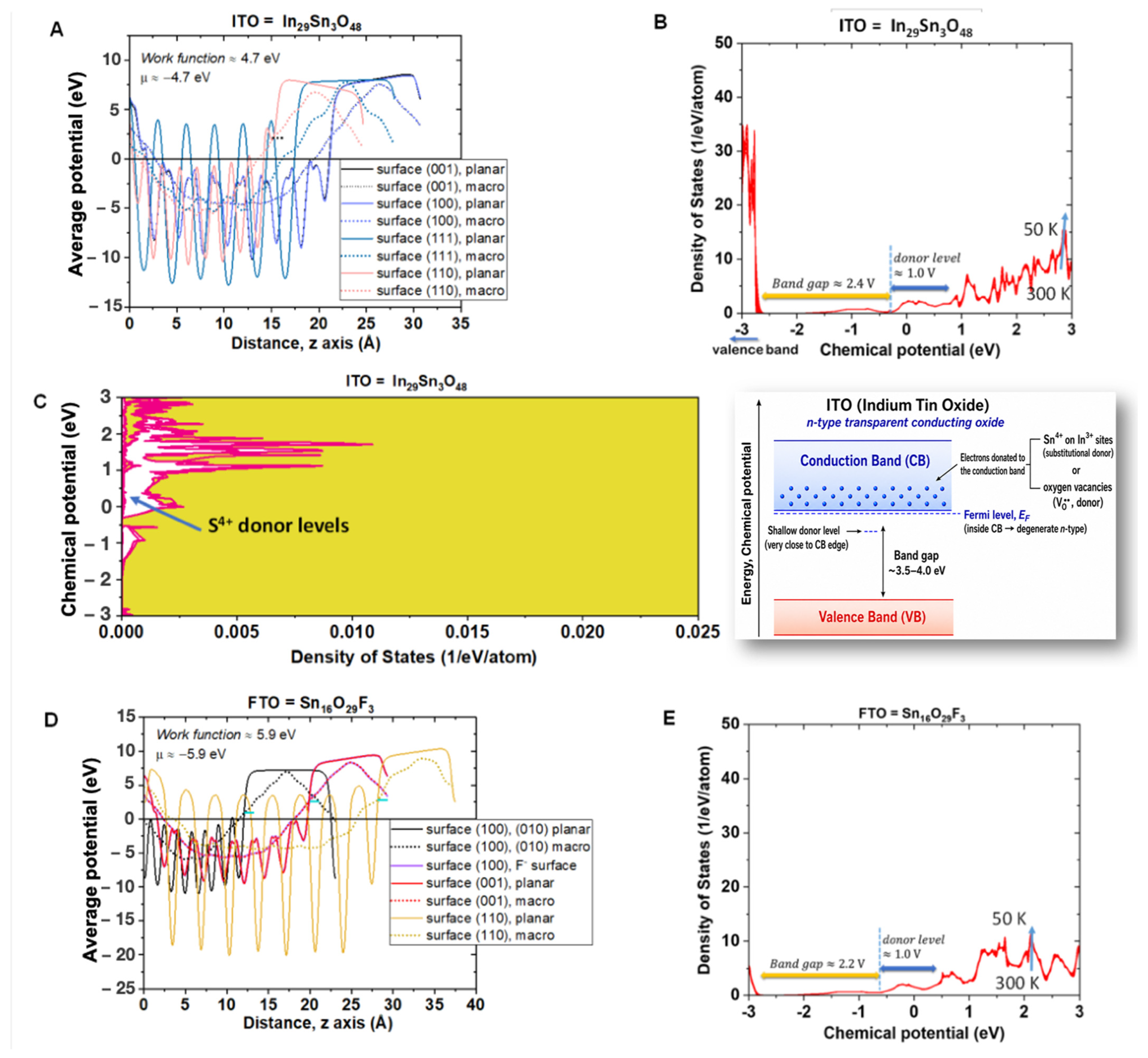
Figure 1. The calculated surface electrostatic potentials and electronic density of states show differences between ITO (In
29Sn
3O
48), and FTO (Sn
16O
29F
3), despite both behaving as degenerately doped n-type transparent semiconductor oxides,
Figure 1.
For ITO, the planar averaged potential exhibits pronounced oscillations across the slab, reflecting the atomic-scale variation in the ionic and electronic charge densities. The macroscopically averaged potential smooths these oscillations and allows the vacuum level to be identified. From the vacuum alignment, a work function of approximately 4.7 eV is obtained, corresponding to an electronic chemical potential of µ ≈ −4.7 eV relative to electrons at rest in a vacuum,
Figure 1A,C. The (001) and (100) surfaces yield broadly similar vacuum levels, although the microscopic potential profiles may differ due to their distinct atomic stacking and terminations, as evidenced by the ITO calculations presented in
Figure 1A, where the most reliable simulated work function is obtained; consequently, chemical potential is the one given by the stack containing a surface dopant (Sn
4+). The work function is determined not only by the bulk Fermi level but also by the surface dipole associated with each crystallographic orientation.
FTO exhibits a higher calculated work function of approximately 5.9 eV, corresponding to µ ≈ −5.9 eV. The (100)/(010), (001), and (110) surfaces show visibly different planar and macroscopic potential profiles, indicating a stronger dependence on facet and surface termination,
Figure 1D. This behavior is consistent with the rutile SnO
2 structure, in which the coordination and density of exposed Sn, O, and F species vary significantly between surfaces. The approximately 1.2 eV difference between the work functions of FTO and ITO places the FTO Fermi level at a deeper absolute energy and may reflect an inadequate positioning of the F
− dopant regarding the surface, in agreement with similar verification for ITO and experimental data. Consequently, the two transparent electrodes are expected to establish different interfacial potential barriers and charge-transfer driving forces when contacted with ZnO or TiO
2.
The total density of states of ITO gives a calculated valence to conduction band separation of approximately 2.4 eV (
Figure 1B,C). This is lower than the commonly reported experimental optical gap of ITO, as expected from the underestimation of semiconductor bandgaps by semilocal density functional approximations. Nevertheless, the calculation reproduces the essential characteristics of the doped oxide. Weak Sn-derived donor states appear close to the conduction band edge, extending over an energy interval of approximately 1.0 eV. These states are more clearly visible in the enlarged low electronic density of states (DOS) representation (
Figure 1B,C).
Substitutional Sn
4+ on In
3+ sites contributes one excess electron per dopant, shifting the Fermi level toward or into the In (5s)-derived conduction band (
Figure 1C). Oxygen vacancies may provide additional donor contributions depending on their local environment and charge state. The finite density of states close to the Fermi level is therefore consistent with the degenerate n-type character of ITO. In this regime, the lowest conduction band states are partially occupied, which may also shift the apparent optical absorption edge to higher energies through the Burstein–Moss effect. Oxygen vacancies are discussed here only as a possible additional donor mechanism in experimental ITO; they were not included in the In
29Sn
3O
48 computational model used in this work.
The widely used 90 wt.% In2O3/10 wt.% SnO2 ITO formulation corresponds to approximately 9.3 at.% Sn on the cation sublattice, closely matching the 9.4 at.% represented by In29Sn3O48 and is, therefore, used herein for simulations of the ITO.
A similar electronic structure was obtained for FTO. The calculated valence to conduction band separation is approximately 2.2 eV, again lower than the experimental optical gap generally reported for fluorine-doped SnO
2 (
Figure 1E). Fluorine substitution on oxygen sites,
, provides one excess electron per substitution and generates donor-related states close to the Sn (5s)-dominated conduction band edge. These donor states extend over an interval of approximately 1.0 eV, while the finite DOS around the Fermi level confirms that the simulated FTO composition is also degenerately n-type (
Figure 1E).
Although the calculated electronic gaps of ITO and FTO are similar, their absolute energy-level positions differ. FTO combines a deeper chemical potential and larger work function with a donor-rich conduction band region, whereas ITO displays a shallower chemical potential and lower work function. This distinction is highly relevant for transparent-electrode/electron-transport-layer heterojunctions. The lower work function of ITO should favor electron donation to an adjacent electron-accepting oxide more strongly than FTO, although the final interfacial charge redistribution will also depend on the electron affinity, surface defects, morphology, and chemical potential of the deposited ZnO or TiO2 layer.
The DOS and surface potential energy calculations are therefore complementary. The DOS describes the distribution of available electronic states relative to the Fermi level, whereas the vacuum-referenced surface calculations establish their absolute energetic position. Together, the results show that ITO and FTO are both degenerate n-type transparent conducting oxides, but they are not electronically equivalent. Their distinct work functions, facet-dependent surface dipoles, and donor-state distributions are expected to produce different band alignment, charge accumulation, and transport behavior at the corresponding oxide interfaces.
To investigate the influence of ETL on TCOs, ZnO and TiO
2 were deposited onto ITO and FTO substrates by drop coating. SEM imaging of the bare substrates, prior to ETL deposition, can be found in
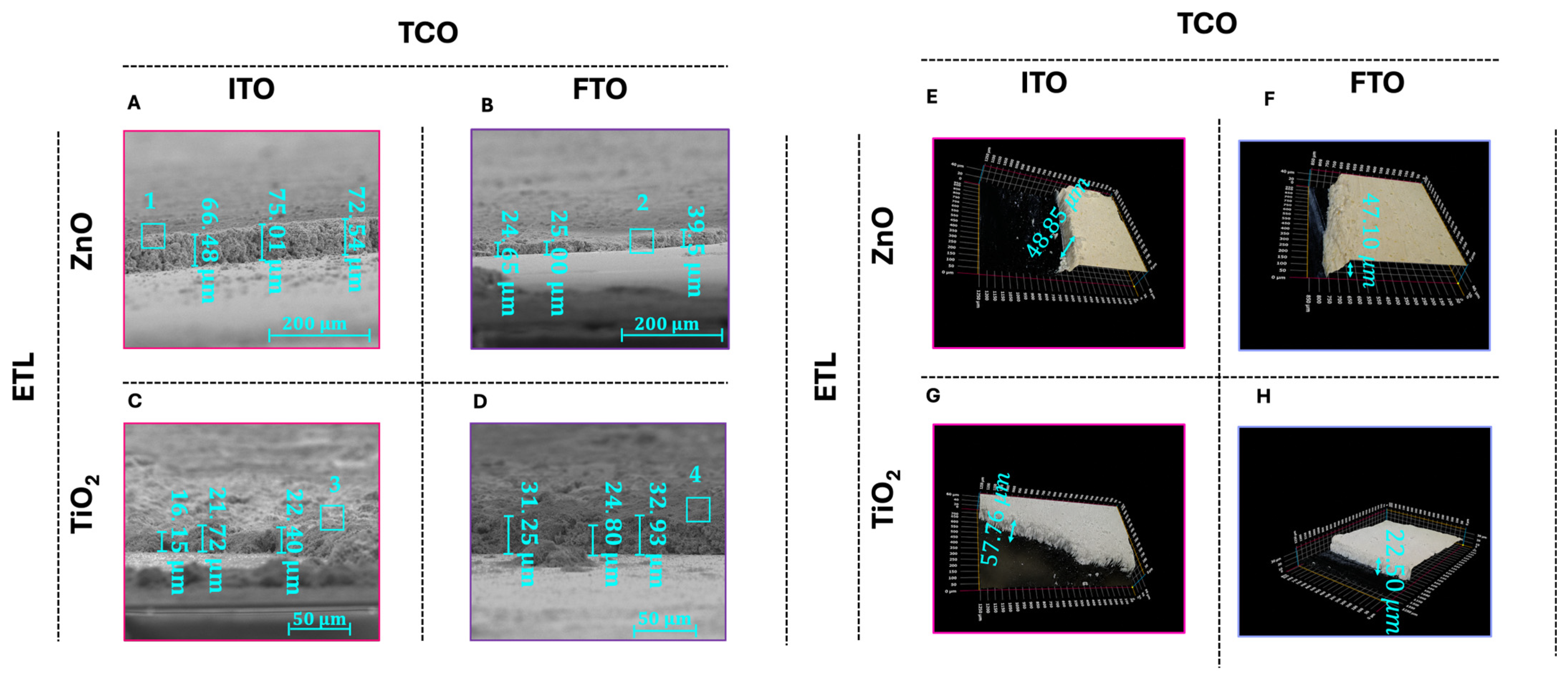
Figure S1A,B, Supplementary Information. Since the thickness of the ETL strongly influences the optical and electrical performance of the final device, the deposited layers were characterized by SEM,
Figure 2A–D, and surface reconstruction using a motorized digital microscope,
Figure 2E–H and
Figure S1C–F, Supplementary Information. For comparison, an additional flexible PET-ITO substrate was also characterized and is presented in
Figure S2, Supplementary Information.
In both cases, ZnO-coated and TiO
2-coated TCOs show comparable layer thicknesses (between 20 and 75
,
Figure 2 and
Figure S2B–E, Supplementary Information), although the TiO
2 coatings were consistently thinner than the ZnO coatings. Furthermore, the SEM images reveal significant differences in the morphology of the deposited layers. The ZnO coating (
Figure 2A,B) exhibits a denser, more compact and robust microstructure, whereas the TiO
2 layer (
Figure 2C,D) appears less consolidated, presenting a rougher surface morphology and a less homogeneous structure. Energy-dispersive X-ray spectroscopy (EDX) analysis of the deposited oxide layers confirmed the absence of detectable contamination (
Table S1, Supplementary Information).
Sheet resistance and Hall effect measurements were performed on the ETL-coated TCOs using a four-point gold probe configuration. From these measurements, the sheet resistance, charge carrier concentration, and carrier mobility were determined for all samples (
Figure 3,
Figures S3 and S4, Supplementary Information). ITO and FTO exhibited the expected behavior of conductive materials, with sheet resistance increasing as the temperature increased (ITO:
Figure S3A–C and FTO:
Figure S3D–F, Supplementary Information). The average sheet resistance calculated over the temperature range from −40 to 100
was approximately 8 Ω/0.12 µm ≈ 67 × 10
6 Ωm
−1 for ITO during both heating and cooling (
Figure S3A, Supplementary Information) and 19 Ω/0.330 µm ≈ 58 × 10
6 Ωm
−1 for FTO,
Figure S3D, Supplementary Information. These values are consistent with the nominal sheet resistance specified by the manufacturer (ITO < 10 Ω and FTO ≈ 15 Ω. Manufacturer information in
Section 3). The calculated charge carrier concentration was negative (e
−) for both materials, corresponding to −5.68 × 10
20 cm
−3 for ITO during both heating and cooling (
Figure S3B, Supplementary Information) and −4.05 × 10
20 cm
−3 for FTO during both heating and cooling,
Figure S3E, Supplementary Information. These results lead measured mobility values, which were also negative for both substrates, as expected, averaging approximately −40 cm
2 V
−1 s
−1 for ITO (
Figure S3C, Supplementary Information) and −23 cm
2 V
−1 s
−1 for FTO,
Figure S3F, Supplementary Information.
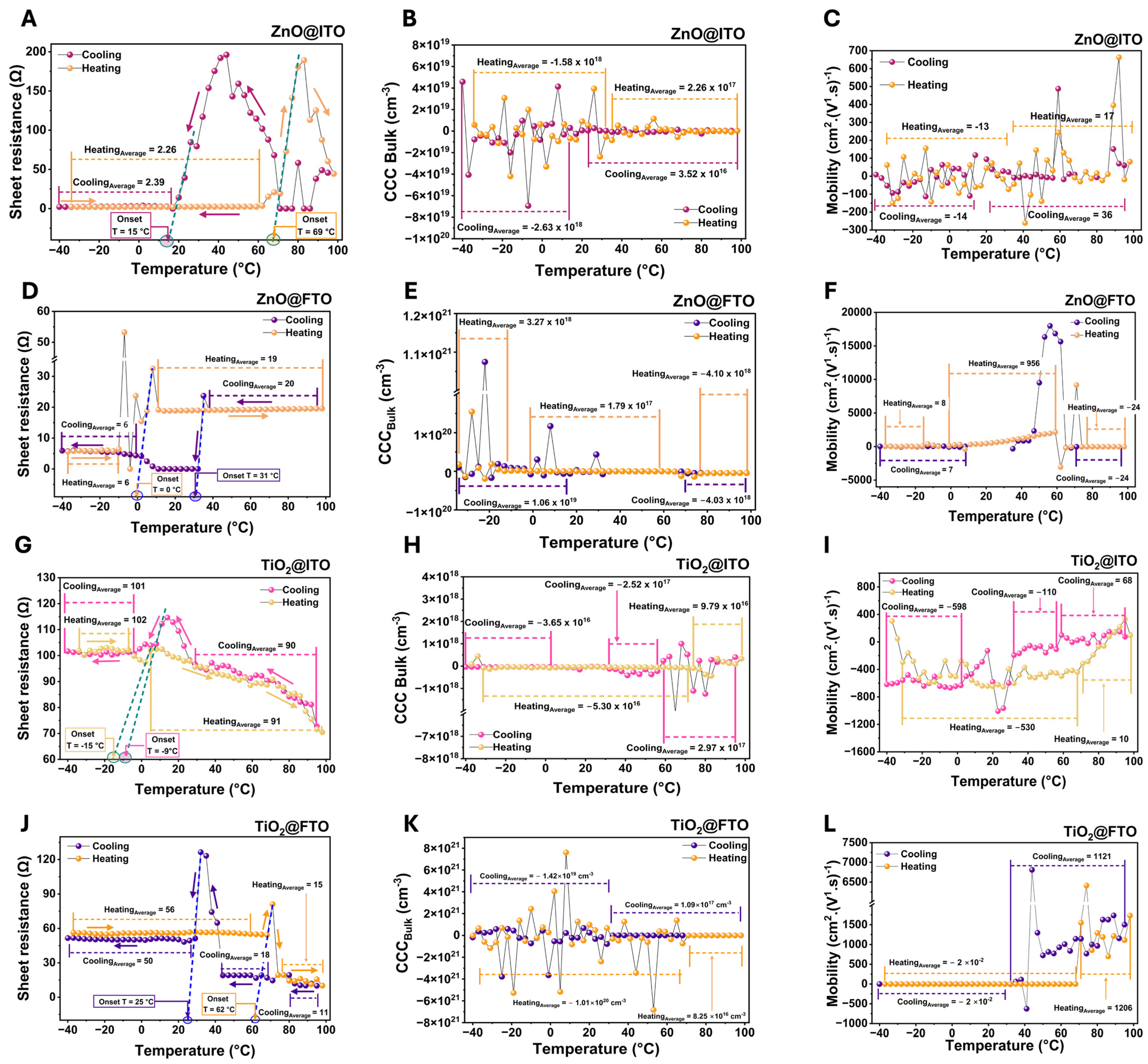
The sheet resistance, charge carrier concentration, and carrier mobility of ZnO-coated ITO are presented in
Figure 3A–C, respectively. During heating, the average sheet resistance remained approximately constant at 2.26 Ω between −40 and 60 °C,
Figure 3A. Since ZnO is a wide-bandgap semiconductor, the dependence of sheet resistance on temperature contrasts with that of the bare TCO substrate (a conductor—with linear dependency between sheet resistance and temperature,
Figure S3A, Supplementary information). At 69 °C, a phase transition induces a sudden shift from a low- to a high-resistance state (
Figure 3A). The sheet resistance reaches a maximum of 200 Ω at 80 °C, subsequently decaying to a value of roughly 50 Ω around 100 °C (
Figure 3A). During cooling, the sheet resistance abruptly increases at 71 °C, reaching a peak of 200 Ω at 45 °C (
Figure 3A). Below 45 °C, the resistance drops sharply, stabilizing at an average of 2.39 Ω between 15 °C and −40 °C (
Figure 3A). The charge carrier concentration and mobility exhibited two distinct temperature regimes during both heating and cooling. During heating, from −40 to 25 °C, the average charge carrier concentration was −1.58 × 10
18 cm
−3, with a corresponding mobility of −13 cm
2 V
−1 s
−1,
Figure 3B,C, confirming n-type conduction dominated by e
−. Above this interval (35 to 100 °C), the average charge carrier concentration changed to 2.26 × 10
17 cm
−3, while the average mobility increased to 17 cm
2 V
−1 s
−1, confirming p-type conduction dominated by h
+. A similar behavior was observed during cooling. From 100 to 30 °C, the average charge carrier concentration and mobility were 3.52 × 10
16 cm
−3 and 36 cm
2 V
−1 s
−1, respectively, whereas from 10 to −40 °C, the values changed to −2.63 × 10
18 cm
−3 and −14 cm
2 V
−1 s
−1,
Figure 3B,C.
In contrast, ZnO-coated FTO (
Figure 3D–F) exhibited a significantly different temperature-dependent response. Compared with its ITO-based counterpart (
Figure 3A), the FTO-based sample exhibited a much more pronounced sheet resistance hysteresis (
Figure 3D). The hysteresis observed for the ZnO-coated ITO sample was less pronounced, consisting of sharp resistance peaks rather than a well-defined hysteresis loop (
Figure 3A). A similarly less defined hysteresis was also observed for the ZnO-coated PET/ITO sample (
Figure S3J, Supplementary Information). These differences can be attributed to the greater thermal stability of the FTO substrate relative to ITO and PET/ITO, which allows the temperature-dependent electrical response of the ZnO@FTO interface to remain more clearly distinguishable throughout the heating and cooling cycles.
The ZnO@FTO system exhibited two distinct transport regimes separated by a clear thermal hysteresis (
Figure 3D). During heating, the sheet resistance remained near 6 Ω between −40 and −10 °C, increased abruptly around 0 °C, and stabilized at approximately 19 Ω from 10 to 100 °C (
Figure 3D). During cooling, it remained close to 20 Ω down to 35 °C before decreasing sharply near 31 °C and returning to approximately 6 Ω below 0 °C (
Figure 3D). Hall measurements confirmed corresponding changes in the dominant carriers (
Figure 3E,F). During heating, hole-dominated conduction was observed below 60 °C, followed by a transition to electron-dominated transport above 75 °C (
Figure 3E,F). During cooling, electron-dominated conduction persisted from 100 to 70 °C, while a pronounced mobility peak appeared between 65 and 45 °C without a comparable increase in carrier concentration (
Figure 3E,F). Below 5 °C, hole-dominated transport was recovered.
For the ZnO-coated TCO substrates, the resistance of the heterojunction decreases at low temperatures (
Figure 3A,E and
Figure S3M, Supplementary Information). This behavior is related to the greater tendency of ZnO to accept electrons from the TCO. The TCO ZnO-coated heterojunction exhibits a more conductor-like temperature dependence, characterized by higher resistance at elevated temperatures and lower resistance at reduced temperatures (
Figure 3A,E and
Figure S3M, Supplementary Information). The resulting charge transfer from the TCO to the ZnO layer increases the electron concentration in the latter, while simultaneously modifying the electrical properties of the ZnO@TCO interface. This process may also be associated with an increased concentration of oxygen vacancies and/or the formation of a Zn-containing alloy or interfacial phase.
A possible microscopic origin of the apparent carrier-type reversal is the temperature-dependent redistribution and charge-state evolution of native and surface defects. In ZnO, oxygen vacancies and Zn-related donor defects may contribute electron states, whereas chemisorbed oxygen and surface hydroxyl species can trap or release carriers as temperature changes. Their relative populations and ionization states can therefore shift the balance of the Hall response and modify the effective interfacial carrier density. In TiO2, thermally activated oxygen-vacancy states provide an analogous donor contribution. Because these processes are coupled to adsorption/desorption and interfacial charge redistribution, they may also produce path-dependent behavior during heating and cooling. This mechanism is proposed as an interpretation of the Hall and resistance data rather than as direct identification of a specific defect species.
For the TiO
2-coated ITO (
Figure 3G–I), the average sheet resistance during heating was 102 Ω between −30 and −10 °C, followed by a phase transition at −15 °C. From 5 to 100 °C, the sheet resistance stabilized with an average value of 91 Ω,
Figure 3G. During cooling, the average sheet resistance was 90 Ω between 100 and 30 °C, followed by a phase transition at −9 °C,
Figure 3G. Between −10 and −40 °C, the sheet resistance stabilized with an average value of 101 Ω,
Figure 3G.
During heating, the average charge carrier concentration between −30 and 70 °C was −5.3 × 10
16 cm
−3, confirming n-type semiconductor conduction dominated by e
−, with a corresponding negative mobility of −530 cm
2 V
−1 s
−1 (
Figure 3H,I). Between 70 and 100 °C, the average charge carrier concentration was 9.69 × 10
16 cm
−3, confirming p-type semiconductor conduction dominated by h
+, with a corresponding mobility of 10 cm
2 V
−1 s
−1,
Figure 3H,I. The average charge carrier concentration during cooling between 100 and 60 °C was 2.97 × 10
17 cm
−3, confirming p-type semiconductor conduction dominated by h
+, with a corresponding positive mobility of 68 cm
2 V
−1 s
−1,
Figure 3H,I. From 60 to 30 °C, the average charge carrier concentration was −2.52 × 10
17 cm
−3, showing n-type semiconductor conduction dominated by e
−, with a corresponding mobility of −110 cm
2 V
−1 s
−1,
Figure 3H,I. From 5 to −40 °C, the average charge carrier concentration was −3.65 × 10
16 cm
−3, with a corresponding mobility of −598 cm
2 V
−1 s
−1,
Figure 3H,I. For comparison, a TiO
2-coated PET/ITO substrate was also characterized by sheet resistance and Hall effect measurements showing very similar behavior,
Figure S3J–L.
Contrary to the behavior observed for the ZnO-coated substrates, all TiO
2-coated substrates exhibited an increase in sheet resistance at low temperatures (
Figure 3G,J and
Figure S3J, Supplementary Information). This trend was consistently observed for the ITO- FTO-, and PET/ITO-based samples, despite the corresponding bare substrates exhibiting a decrease in resistance upon cooling (
Figure S3A–I, Supplementary Information). Therefore, unlike the ZnO-coated systems, the temperature-dependent electrical response of the TiO
2-coated heterojunctions is governed primarily by the TiO
2 layer. As a non-degenerate semiconductor, TiO
2 relies on thermally activated defects, such as oxygen vacancies, to donate electrons to the conduction band. Cooling suppresses this thermal activation, reducing carrier mobility and consequently increasing the resistivity (
Figure 3G,J and
Figure S3J, Supplementary Information). Similarly to the ZnO-coated substrates, the TiO
2-coated FTO sample exhibited a more clearly defined sheet resistance hysteresis than the corresponding ITO- and PET/ITO-based samples, consistent with the greater thermal stability of the FTO substrate. During heating, the TiO
2-coated FTO sheet resistance remained approximately 56 Ω from −40 to 60 °C, before decreasing sharply near 62 °C and reaching an average of 15 Ω, between 75 and 100 °C (
Figure 3J). During cooling, values of approximately 11 and 18 Ω were obtained over the intervals of 100–80 °C and 70–45 °C, respectively. Below the transition near 25 °C, the resistance increased and stabilized at approximately 50 Ω down to −40 °C. The Hall effect results reveal a corresponding reversal in the dominant transport mechanism (
Figure 3K,L). For the heating process, electron-dominated conduction prevailed between −40 and 65 °C, with an average carrier concentration of −1.01× 10
20 cm
−3 and mobility of −2 × 10
−2 cm
2 V
−1 s
−1. Above 70 °C, both parameters became positive, reaching 8.25 × 10
16 cm
−3 and 1206 cm
2 V
−1 s
−1, respectively, indicating hole-dominated transport. For the cooling part, this p-type regime persisted from 100 to 30 °C, with average values of 1.09 × 10
17 cm
−3 and 1121 cm
2 V
−1 s
−1. Below 25 °C, electron-dominated conduction was recovered, with a carrier concentration of −1.42 × 10
19 cm
−3 and mobility of −2 × 10
−2 cm
2 V
−1 s
−1 (
Figure 3K,L).
To investigate the electrochemical behavior of these systems, the chemical potential of the materials was determined using μm-resolution scanning Kelvin probe (μm-SKP) measurements and nm-resolution SKPM. For the μm-resolution measurements, samples with a Cu/ETL-coated TCO/Al architecture were analyzed. The ETL-coated TCO region, approximately 5 mm in length, was exposed to the SKP tip, while the Cu electrode provided the electrical connection to the instrument. The scan was performed from the Cu electrode, across the ETL-coated TCO region, and toward the Al electrode. For the nm-resolution SKP measurements, a 20 × 20 μm2 area of the ETL-coated TCO surface was analyzed.
To establish a reference, the surface chemical potentials of bare ITO, FTO, and PET/ITO were firstly characterized using the same approach (
Figure S5, Supplementary Information). The μm-resolution measurements were performed in a Cu/TCO/Al configuration, whereas the nm-resolution measurements were carried out directly on the bare TCO surfaces (
Figure S5, Supplementary Information).
When incorporated into the Cu/ITO/Al configuration, electron transfer occurs from Al toward ITO and Cu (
Figure S5A, Supplementary Information). The Cu electrode is electrically connected to the SKP, allowing electron transfer through Cu and from Cu to the SKP. In the 1st frame, the chemical potentials of ITO and Cu align at an average value of approximately −0.19 V vs. SHE (−4.25 eV), while the Al potential remains at −0.82 V vs. SHE (−3.62 eV) (
Figure S5A, Supplementary Information). In the third frame, the ITO and Cu potentials align at approximately −0.05 V vs. SHE (−4.39 eV), approaching the chemical potential of bare ITO measured by nm-resolution SKP (−0.01 V vs. SHE, −4.43 eV,
Figure S5B, Supplementary Information, in agreement with the literature as reported in
Table 1), while the Al potential shifts to −0.60 V vs. SHE (−3.84 eV). These results indicate that electrons are transferred from Al through ITO toward Cu and subsequently from Cu to the SKP.
For the Cu/FTO/Al configuration, the Al potential remains at −0.65 V vs. SHE (−3.79 eV) across all frames. Meanwhile, the chemical potentials of FTO and Cu align at approximately 0.15 V vs. SHE (−4.59 eV) in the first measurement and 0.04 V vs. SHE (−4.48 eV) in the third (
Figure S5C, Supplementary Information). In the nm-SKP measurements, bare FTO exhibits a potential of 0.30 V vs. SHE (−4.74 eV) (
Figure S5D, Supplementary Information). Considering that Cu also has an individual potential of approximately 0.30 V vs. SHE (−4.74 eV) [
31,
39,
48], their shift to 0.04 V vs. SHE (−4.48 eV) in the Cu/FTO/Al heterojunction indicates electron transfer from Al to Cu and FTO. The Al chemical potential shows periodic oscillations with a wavelength (
) of approximately 1350 μm,
Figure S5C Supplementary Information. A similar phenomenon has previously been reported for Al in a Cu/SiO/Al configuration, exhibiting a comparable oscillation wavelength [
45]. FTO consists predominantly of F-doped SnO
2 and therefore contains a substantially higher SnO
2 fraction than ITO. Since Sn and Si belong to the same group of the periodic table and both SnO
2 and SiO behave as n-type semiconductors, the similarity between these systems may account for the comparable oscillatory behavior. Furthermore, the metallic nature of Al, together with its high and flat electronic density of states above and below the Fermi level, enables efficient charge exchange with the adjacent semiconductor while accommodating a broad range of measured chemical potentials, from approximately −1 V vs. SHE (−3.44 eV) to +0.3 V vs. SHE (−4.74 eV) [
31,
39,
48].
The Cu/PET/ITO/Al system exhibited a progressive shift in the PET/ITO chemical potential toward more negative values over successive measurements, reaching approximately −0.30 V vs. SHE (−4.14 eV) in the final measurement (
Figure S5E, Supplementary Information). Electrons flow from Al through PET/ITO toward Cu, as indicated by the Al potential becoming considerably more positive than its expected value of approximately −1 V vs. SHE (−3.44 eV). However, the absence of potential alignment between PET/ITO and Cu suggests that electron transport from PET/ITO to the Cu electrode is limited. Consequently, electrons accumulate on the PET/ITO surface, shifting its potential from the bare value of 0.57 V vs. SHE (−5.01 eV) to increasingly negative values (
Figure S5F, Supplementary Information). This behavior is associated with the higher effective resistance of the flexible conductive layer, as supported by the sheet resistance measurements (PET/ITO, ITO thickness: 800 Ω/0.200 µm = 4000 × 10
6 Ωm
−1,
Figure S3G; ITO: 8 Ω/0.140 µm = 67 × 10
6 Ωm
−1,
Figure S3A; and FTO: 58 × 10
6 Ωm
−1,
Figure S3D, Supplementary Information) and coating discontinuities or inhomogeneities observed by SEM (
Figure S2A, Supplementary Information).
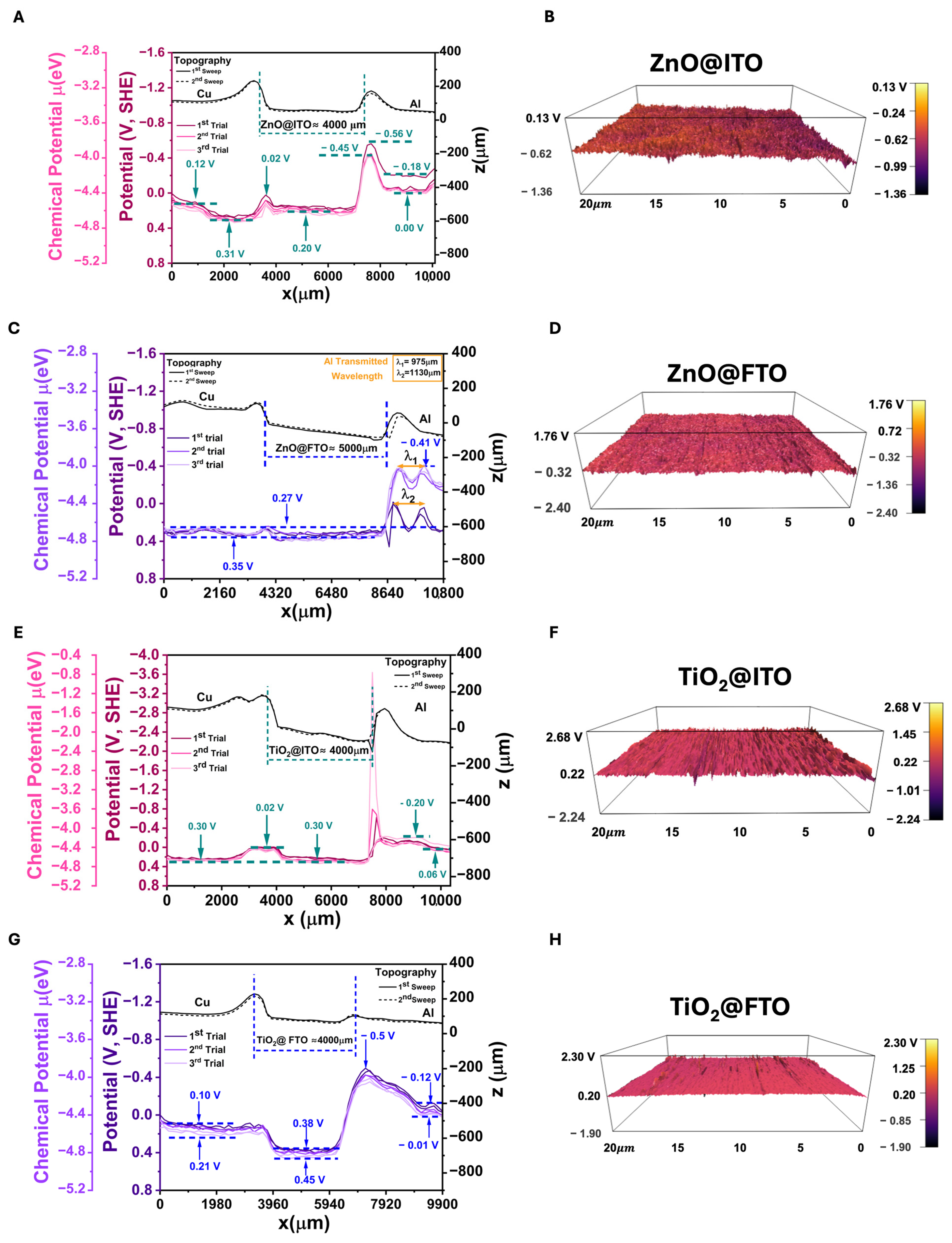
In the Cu/ZnO@ITO/Al architecture, the Cu potential initially measures approximately 0.12 V vs. SHE (−4.56 eV), due to the electrical connection between the Cu electrode and the SKP system, which promotes charge exchange as the electrode and instrument approach potential equilibration (
Figure 4A). The Cu chemical potential then stabilizes at approximately 0.31 V vs. SHE (−4.75 eV), consistent with the expected value for Cu chemical potential [
31,
39,
48],
Figure 4A. At nanometer resolution, ZnO@ITO displays a chemical potential of −0.62 V vs. SHE (−3.82 eV) (
Figure 4B), substantially more negative than the values of bare ITO (0.30 V vs. SHE, −4.74 eV) and ZnO (0.40 V vs. SHE, −4.84 eV [
31]). This shift suggests that contact between ZnO and ITO promotes electron transfer from ITO to ZnO, leading to electron accumulation and negative charging at the ZnO surface, when bare,
Figure 4B. When the ZnO@ITO heterojunction is incorporated into the Cu/ZnO@ITO/Al architecture, electron tunneling occurs among the three components until their chemical potentials approach “equilibrium”. The resulting redistribution of charge explains the approximately 0.8 eV difference between the chemical potential of the isolated ZnO@ITO interface and that measured in the complete Cu/ZnO@ITO/Al architecture.
In the Cu/ZnO@ITO/Al configuration, additional charge redistribution occurs with ZnO@ITO exhibiting an average potential of approximately 0.20 V vs. SHE (−4.64 eV),
Figure 4A. Distinct negative potential peaks are observed at both the Cu/ZnO@ITO and Al/ZnO@ITO interfaces, indicating localized electron accumulation,
Figure 4A. The most pronounced accumulation occurs at the Al/ZnO@ITO interface, where the potential reaches −0.56 V vs. SHE (−3.88 eV) during the first measurement and stabilizes at approximately −0.45 V vs. SHE (−3.99 eV) in the second and third measurements,
Figure 4A. Likewise, the Al potential initially stabilizes at approximately −0.18 V vs. SHE (−4.26 eV) before progressively approaching 0.00 V vs. SHE (−4.44 eV) in subsequent measurements. This evolution suggests gradual equilibration among the chemical potential of the electrode, sample, and SKP system (
Figure 4A), with electrons flowing, from Al and ZnO@ITO toward the SKP through the Cu connection.
For the Cu/ZnO@FTO/Al configuration, the chemical potentials of Cu and ZnO@FTO were aligned throughout the sample, reaching a common value of approximately 0.35 V vs. SHE (−4.79 eV) in the first measurement and 0.27 V vs. SHE (−4.71 eV) in subsequent measurements (
Figure 4C). Although the initial potential alignment across the sample suggests that the components approached electrochemical equilibrium at approximately 0.35 V vs. SHE (−4.79 eV), the strong electron-accepting character of ZnO promotes electron transfer from the FTO to the ZnO layer, driving the potential toward more negative values (
Figure 4C). This process is further assisted by charge exchange between the sample and the SKP during the measurement. Consistent with this interpretation, the
nm-SKPM measurements show that ZnO@FTO exhibits a potential of −0.32 V vs. SHE (−4.12 eV) (
Figure 4D), which is more negative than both bare FTO and bare ZnO, providing independent evidence of charge redistribution within ZnO@FTO, as previously observed in the ZnO@ITO system (
Figure 4B). A small peak of potential was observed at the Cu/ZnO@FTO interface (
Figure 4C), although its amplitude was lower than that observed for ZnO@ITO (
Figure 4A). In contrast, a pronounced potential wall appeared at the ZnO@FTO/Al interface (
Figure 4C), accompanied by periodic oscillations extending across the Al region, as previously observed in the bare FTO,
Figure S5C, Supplementary Information. The wavelengths of Al oscillations in Cu/ZnO@FTO/Al were similar across the measurements, ranging from approximately 975 μm in the first measurement to 1130 μm in the second and third measurements (
Figure 4C).
In the case of the Cu/TiO
2@ITO/Al configuration (
Figure 4E), a similar tendency to that observed for the ZnO@ITO system is found (
Figure 4A), with the chemical potentials of the TiO
2@ITO layer and Cu aligning. The Cu chemical potential averages approximately 0.27 V vs. SHE (−4.71 eV), while the TiO
2@ITO layer exhibits an average chemical potential of 0.30 V vs. SHE (−4.74 eV) (
Figure 4E). At the nanoscale SKP, measurements show that the TiO
2@ITO surface exhibits a potential of 0.22 vs. SHE (−4.66 eV) (
Figure 4F). Unlike the ZnO@ITO system, the absence of a pronounced shift in the TiO
2 surface potential indicates that no significant electron transfer occurs from the ITO to the TiO
2 layer. Consequently, the measured surface potential remains close to the intrinsic chemical potential of TiO
2 rather than exhibiting the negative shift associated with interfacial charge redistribution (
Figure 4F). This interpretation is further supported by the agreement between the measured surface potential and values reported in the literature for TiO
2 [
39]. Additionally, as observed for the previous systems, charge accumulation regions are detected at both the Cu/TiO
2@ITO and Al/TiO
2@ITO interfaces, with the most pronounced potential peak occurring at the Al/TiO
2@ITO interface (
Figure 4E). Unlike ZnO, TiO
2 exhibits a lower ability to conduct electrons across its surface. Consequently, TiO
2 cannot efficiently channel the electrons originating from the Al substrate through its surface toward the remaining layers, resulting in enhanced charge accumulation at the Al/TiO
2@ITO interface (
Figure 4E). The ZnO@ITO/PET and TiO
2@ITO/PET systems exhibit the same behavior, with ZnO showing a greater ability to conduct electrons across its surface than TiO
2 (
Figure S6A–D, Supplementary Information).
For the Cu/TiO
2@FTO/Al configuration, the TiO
2@FTO layer exhibited a potential of approximately 0.45 V vs. SHE (−4.89 eV) (
Figure 4G), whereas the nanometric measurement holds a lower value of 0.20 V vs. SHE (−4.64 eV) (
Figure 4H). Once again, the SKP measurement predominantly reflects the TiO
2 surface, as this value corresponds to that expected for TiO
2 alone [
36]. Compared with the potential of bare FTO 0.33 V vs. SHE (−4.77 eV) (
Figure S5D, Supplementary Information), the nanometric result 0.20 V vs. SHE (−4.64 eV) (
Figure 4H) indicates only a small contribution from the underlying FTO and limited electron transfer to TiO
2. Across successive SKP measurements, the chemical potentials of all components shifted downward, corresponding to increasingly positive potentials: from 0.10 to 0.21 V vs. SHE (−4.54 to −4.65 eV) for Cu, from 0.38 to 0.45 V vs. SHE (−4.82 to −4.89 eV) for TiO
2@FTO, and from −0.12 to −0.01 V vs. SHE (−4.32 to −4.43 eV) for Al,
Figure 4G. This coordinated shift is consistent with progressive electron transfer towards the Cu/SKP connection as the system becomes more positive and tries to align the potentials. Compared with ZnO, TiO
2 appears less effective at accepting and retaining electrons from FTO, limiting negative surface charging and interfacial charge redistribution (
Figure 4G). The more pronounced resistive character of the TiO
2@FTO junction, shown in sheet resistance measurements (
Figure 3G,J), may restrict lateral charge transport toward the other materials.
The optical response of the bare TCO substrates is presented in
Figure S7A–C (Supplementary Information). PET/ITO, ITO and FTO glass exhibit high transparency throughout the visible region, with average transmittance values of approximately 84.2%, 83.2% and 79.4%, respectively, while maintaining low average reflectance (~10%) and absorptance below 11%. Within the UV region of the measured spectral range, all three substrates show a pronounced variation in absorptance and transmittance, consistent with the wide optical bandgaps reported for ITO and FTO, typically around 3.82–4.35 eV [
5,
7,
8], which shift their fundamental absorption toward shorter wavelengths.
Following the deposition of TiO
2 and ZnO, the optical response changed considerably (
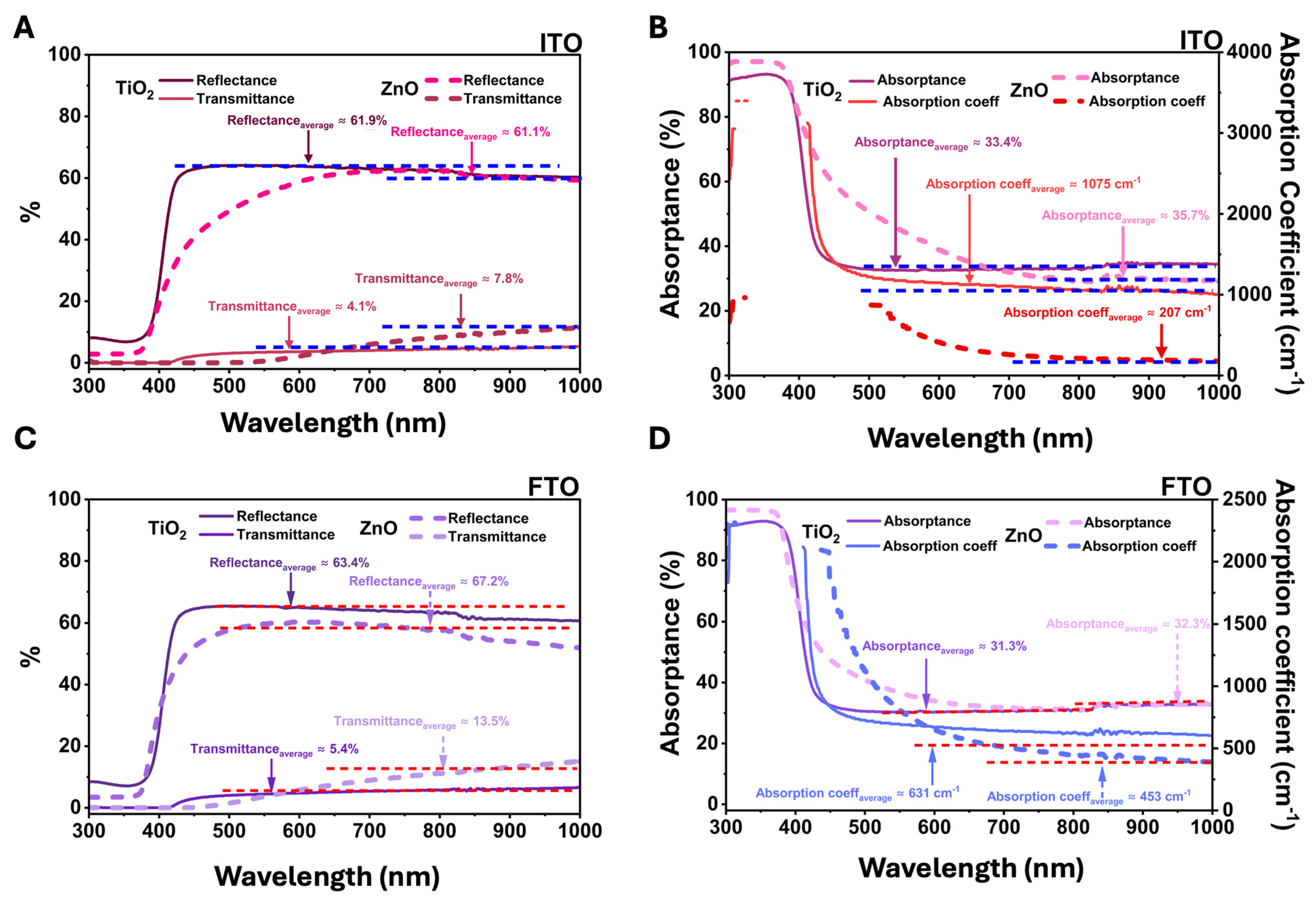
Figure 5). All three substrates exhibited a significant reduction in transmittance and a simultaneous increase in reflectance (
Figure 5) compared with their corresponding bare substrates,
Figure S7A–C (Supplementary Information). The average reflectance increased to approximately 55–67% (
Figure 5A,B and
Figure S7D), whereas the transmittance decreased to values between 4.1 and 13.5% (
Figure 5A,B and
Figure S7D), depending on the deposited oxide and substrate. This behavior is expected considering the incorporation of relatively thick oxide layers of ~30–65 μm, as observed in
Figure 2,
Figures S1 and S2, Supplementary Information), which substantially modify the interaction of light with the TCO surface. The ZnO and TiO
2 ETLs were fabricated by the drop coating deposition method, which, due to experimental limitations, did not allow for a significant reduction in layer thickness. Increasing the ETL thickness generally reduces optical transmittance, as widely reported in the literature. However, the objective of this work was not to optimize the thickness of the ETLs for photovoltaic device applications, but rather to investigate the interfacial interactions between the ETL materials and the TCO substrates. Consequently, the selected thicknesses were considered appropriate for the intended purpose of this study. The thickness values obtained from SEM and optical-microscope edge profiles are not identical because the drop-coated layers are spatially non-uniform and the two techniques probe different local regions and geometrical definitions of the coating edge. Accordingly, the reported values should be interpreted as representative local/average thicknesses rather than as a uniform film thickness over the entire sample.
Since the transmittance and reflectance were measured simultaneously and directly using a UV–Vis spectrometer, these data could not be normalized. However, the absorptance can be normalized to obtain the absorption coefficient, allowing a qualitative comparison of the influence of layer thickness,
Figure 5B,D and
Figure S7E, Supplementary Information. The absorption coefficient was calculated using the following equation,
, where d is thickness, R is reflectance and T is transmittance (R and T were directly measured). It is important to note that, for all oxide/TCO combinations, the absorption coefficient cannot be calculated in the 300–400 nm wavelength range because the measured transmittance is zero. This behavior arises from the combined effect of the relatively large oxide layer thickness and the intrinsic bandgap of the oxide materials, which results in complete absorption of the incident light within the UV region. This behavior can be described by the following equation,
. On ITO, the average absorption coefficient was approximately 1075 cm
−1 for TiO
2 and 207 cm
−1 for ZnO (
Figure 5B), whereas on PET/ITO, the corresponding values were 304 and 228 cm
−1, respectively (
Figure S7E). In contrast, the absorption coefficients on FTO have a smaller gap between oxides, averaging 631 cm
−1 for TiO
2 and 453 cm
−1 for ZnO (
Figure 5D).
The use of absorptance and the derived absorption coefficient in this work is intended as a comparative treatment rather than a determination of intrinsic bulk optical constants. Because the drop-coated layers are rough, non-uniform, and optically scattering, the simple thickness normalization does not fully account for diffuse reflection, multiple scattering, porosity, or local variations in optical path length. Consequently, the calculated values should be interpreted as effective absorption coefficients that facilitate comparison among the deposited oxide/TCO systems. Here, “normalization” refers to accounting for the optical path length; the absorption coefficient is derived from the measured R and T values together with the coating thickness using the stated attenuation expression, rather than by direct division of absorptance by thickness.
On the three substrates, ZnO consistently exhibited higher average transmittance than TiO
2—7.8% and 4.1% for ITO (
Figure 5A), 13.5% and 5.4% for FTO (
Figure 5C) and 11.2% and 4.7% for PET/ITO, respectively (
Figure S7D)—while the average absorptance remained similar for both ZnO and TiO
2 oxides—35.7 and 33.4% for ITO (
Figure 5B), 32.3 and 31.3% for FTO (
Figure 5D) and 28.3 and 30.5% for PET/ITO, respectively (
Figure S7E). At shorter wavelengths, the coated systems exhibited high absorptance, which gradually decreased with increasing wavelength before stabilizing throughout the visible region (
Figure 5). This behavior is consistent with the wide bandgaps of TiO
2 and ZnO, commonly reported at approximately 3.0–3.8 eV [
4,
21,
25,
45].
The observed optical differences cannot be attributed solely to variations in coating thickness, as they remain evident in the thickness-normalized absorption coefficients, particularly for ITO and PET/ITO (
Figure 5B,D and
Figure S7E, Supplementary Information). The SEM images reveal clear differences in morphology, with ZnO forming a denser, more compact, robust layer, whereas TiO
2 exhibits a rougher and less homogeneous surface (
Figure 2 and
Figure S2B–E). These morphological differences indicate that in addition to thickness, the microstructure of the deposited oxide layers plays an important role in determining the optical response of the ETL@TCO systems. Nevertheless, ZnO appears to be the most promising ETL for future photosensitive devices, as it transmits more light to the photoactive layer than TiO
2. This is observed despite the ZnO layer being thicker and denser, while still exhibiting higher transmittance, lower absorptance and lower reflectance than TiO
2.
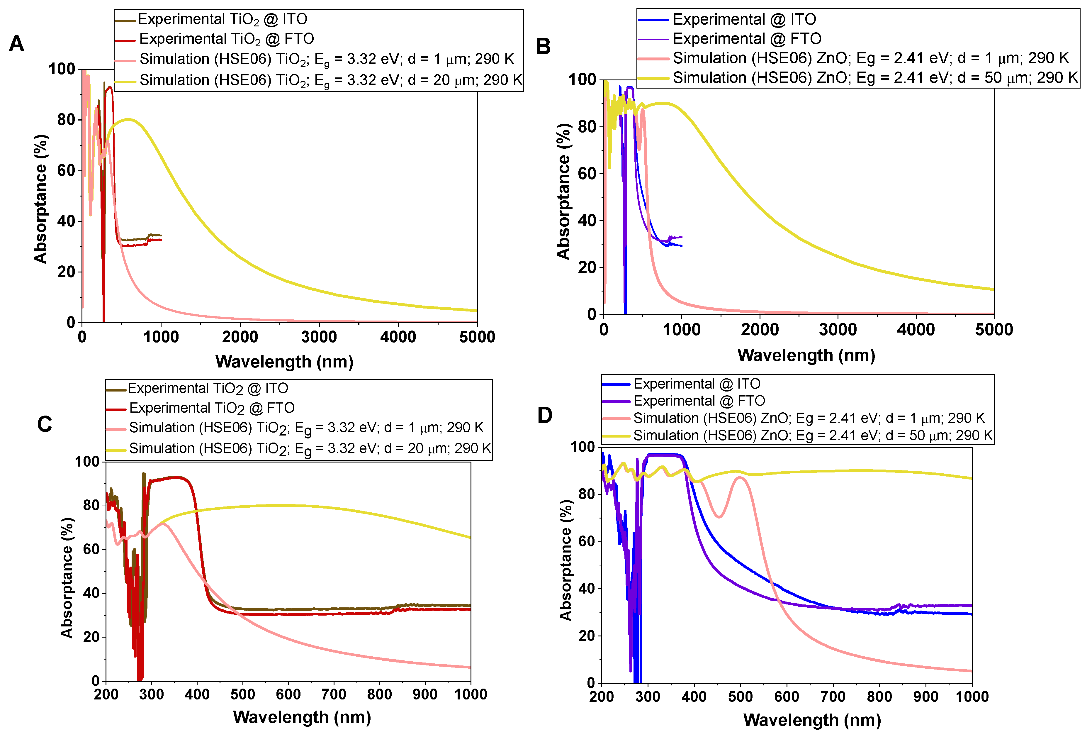
Figure 6 compares the experimental absorptance spectra of the oxide-coated transparent conducting substrates with optical simulations based on the calculated HSE06 bandgaps. The comparison is useful because it separates two contributions that are experimentally superimposed:
(1) the intrinsic optical response expected from the semiconductor bandgap and
(2) the additional absorptance introduced by the conducting substrate, defects, thickness, scattering, and possible interfacial effects.
For the TiO2-based samples, the experimental spectra of TiO2@ITO and TiO2@FTO show strong absorptance in the ultraviolet region, followed by a rapid decrease toward the visible range. This behavior is consistent with the wide-band-gap nature of TiO2, for which the HSE06 calculation gives Eg = 3.32 eV. The corresponding absorption edge is expected in the near-ultraviolet, around 370–380 nm. The experimental spectra show intense features below approximately 400 nm, which agree with the onset of interband absorption in TiO2. However, the measured spectra do not follow the ideal simulated curves exactly. In particular, the experimental absorptance remains at a nearly constant level of about 30–35% at longer wavelengths. This residual absorptance is likely not due to the intrinsic TiO2 bandgap alone, but rather to contributions from the ITO/FTO substrates, free-carrier absorption, optical scattering, surface roughness, film thickness inhomogeneity, and possible defect or interfacial states.
The comparison between the 1 and 20 μm TiO2 simulations further illustrates the strong effect of optical path length. The thinner simulated layer shows a sharp decay after the band edge, whereas the thicker simulated layer produces a broad absorption tail extending into the near-infrared. The experimental spectra are much closer to the film response near the absorption edge but retain a finite long wavelength background. This indicates that the samples behave optically as absorbing oxide coatings on conducting transparent substrates rather than as ideal bulk TiO2 absorbers.
For the ZnO-based system, the HSE06 bandgap calculated in the simulations is Eg = 2.41 eV, corresponding to an absorption onset shifted to longer wavelengths compared with TiO2. The simulated ZnO spectra therefore show a broader response extending further into the visible region. The experimental spectra measured on ITO and FTO also show strong absorption and sharp spectral features in the ultraviolet–visible region, but again the agreement with the ideal simulations is only qualitative. In the 200–1000 nm region, the experimental curves display pronounced structure between approximately 250 and 400 nm, followed by a decrease toward a residual absorptance level. This suggests that the measured response is controlled not only by ZnO interband transitions but also by the transparent conducting substrate and by additional optical losses.
Standard HSE06 with the conventional 25% screened exact-exchange fraction is known to underestimate the bandgap of stoichiometric Wurtzite ZnO. Reported standard HSE06 values around 2.4–2.5 eV [
49] are consistent with the present value of 2.41 eV, whereas reproducing the experimental optical gap near 3.2–3.4 eV generally requires a larger, material-specific exact-exchange fraction or a higher-level quasiparticle treatment. No defects, dopants, oxygen vacancies, or non-stoichiometric ZnO configurations were included here. The simulated spectrum is therefore interpreted as the internally consistent optical response of the standard HSE06 electronic structure, with emphasis on spectral shape and relative trends rather than exact reproduction of the experimental absorption onset.
The difference between ITO and FTO is also relevant. ITO is a degenerately doped n-type transparent conducting oxide, and its high free-electron concentration can introduce free-carrier absorption, especially toward longer wavelengths. FTO is also a doped transparent conducting oxide, but with a different carrier concentration, defect chemistry, and surface morphology. Therefore, even when the same oxide coating is considered, the substrate can modify the apparent absorptance through changes in reflectance, roughness, carrier absorption, and interface quality. The experimental differences between the ITO- and FTO-based samples should therefore be interpreted as a combined effect of the oxide layer and the conducting substrate.
The magnified spectra in
Figure 6C,D emphasize that the ultraviolet–near-visible region is the most diagnostic part of the measurement. In this range, the experimental features coincide with the expected band-edge absorption of the oxide coatings. For TiO
2, the absorption onset is consistent with a wide-gap semiconductor absorbing mainly in the ultraviolet. For ZnO, the lower simulated bandgap produces absorption extending further into the visible range. Nevertheless, the intensity and shape of the experimental curves deviate from the ideal HSE06-based simulations, confirming that real films contain additional optical contributions that are absent from the simplified model.
The results show that the calculated bandgaps correctly capture the expected spectral hierarchy: (1) TiO2 behaves as a wider-gap ultraviolet absorber, whereas (2) ZnO displays a lower-energy absorption onset. The simulations reproduce the main band-gap-controlled absorption trends, while the experimental spectra reveal the importance of film/substrate effects, defect states, thickness, scattering, and free-carrier absorption. Thus, the combined experimental/computational analysis supports the assignment of the dominant optical transitions while highlighting that transparent conducting oxide substrates cannot be treated as optically passive supports.



 ,
,