
Strategies and Methods for Upscaling Perovskite Solar Cell Fabrication from Lab-Scale to Commercial-Area Fabrication

Abstract
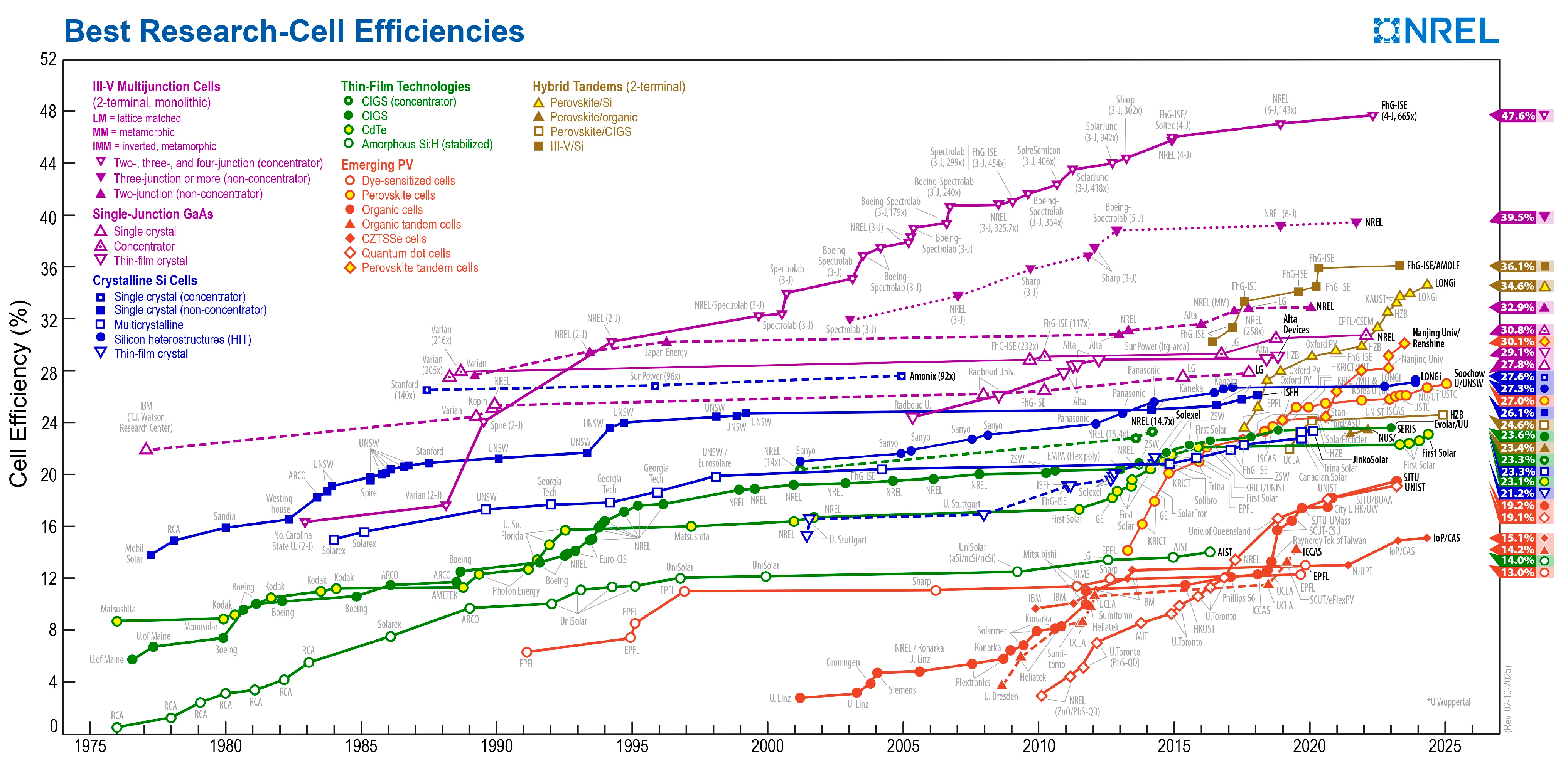
1. Introduction
2. Architecture of Perovskite Devices
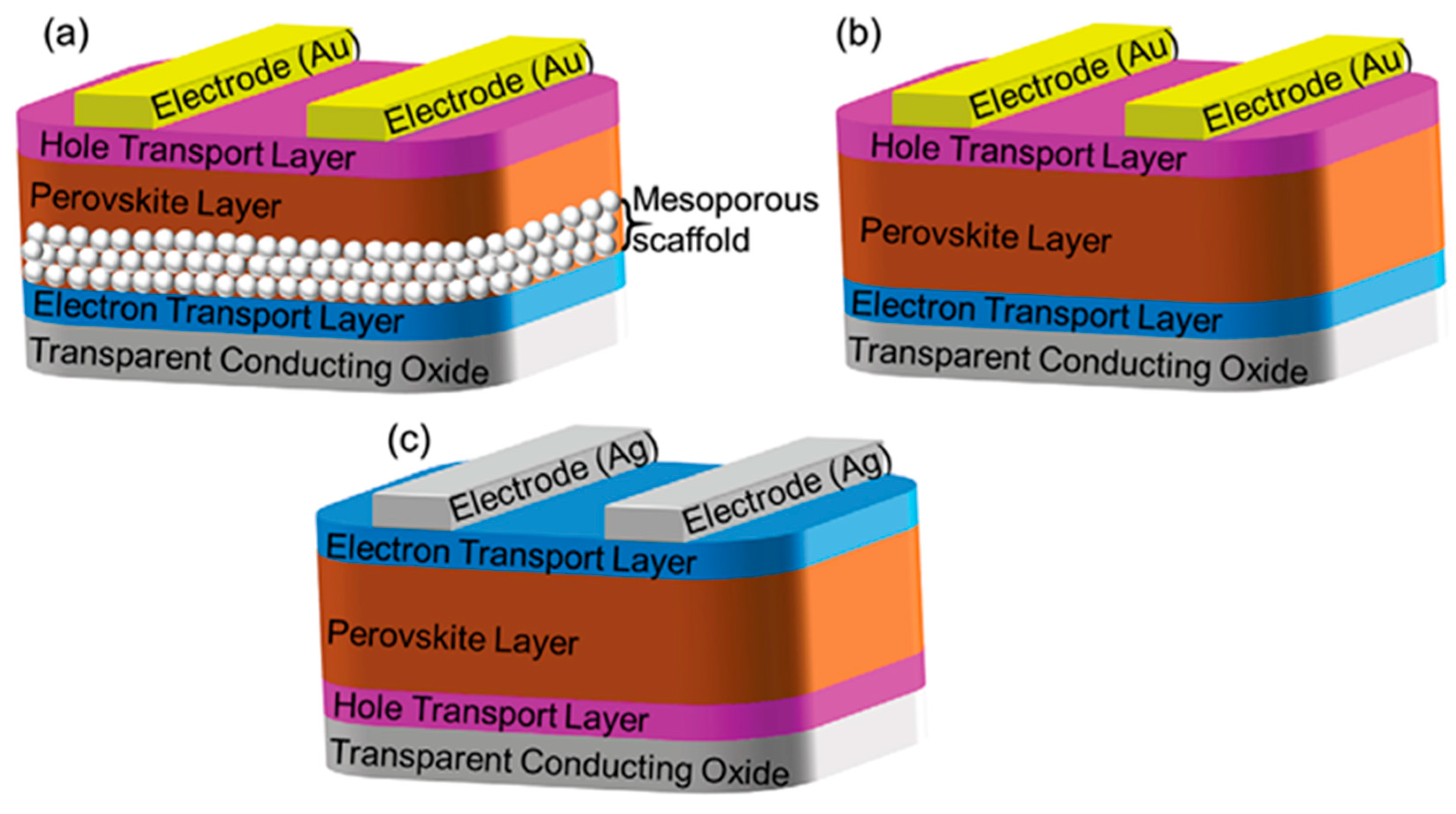
2.1. Architecture of PSCs
2.2. Architecture of PSMs
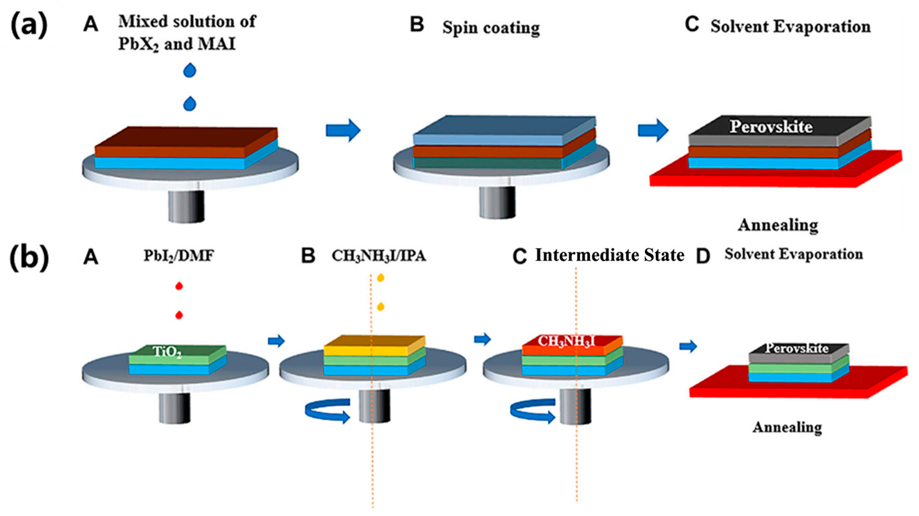
3. Nucleation Process of Perovskite
4. Fabrication of Perovskite Devices, from Small- to Large-Area Fabrication
4.1. Spin-Coating
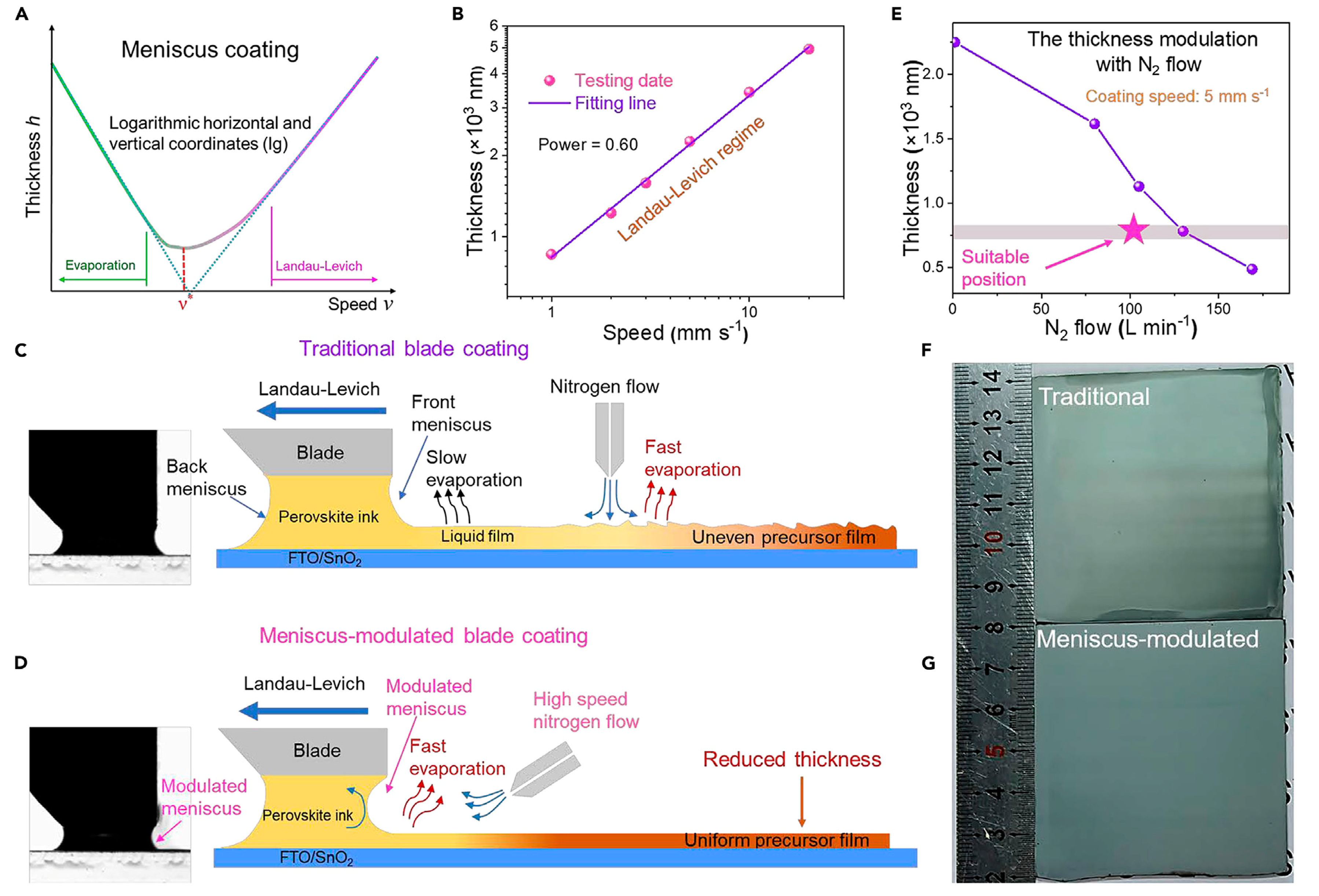
4.2. Blade Coating
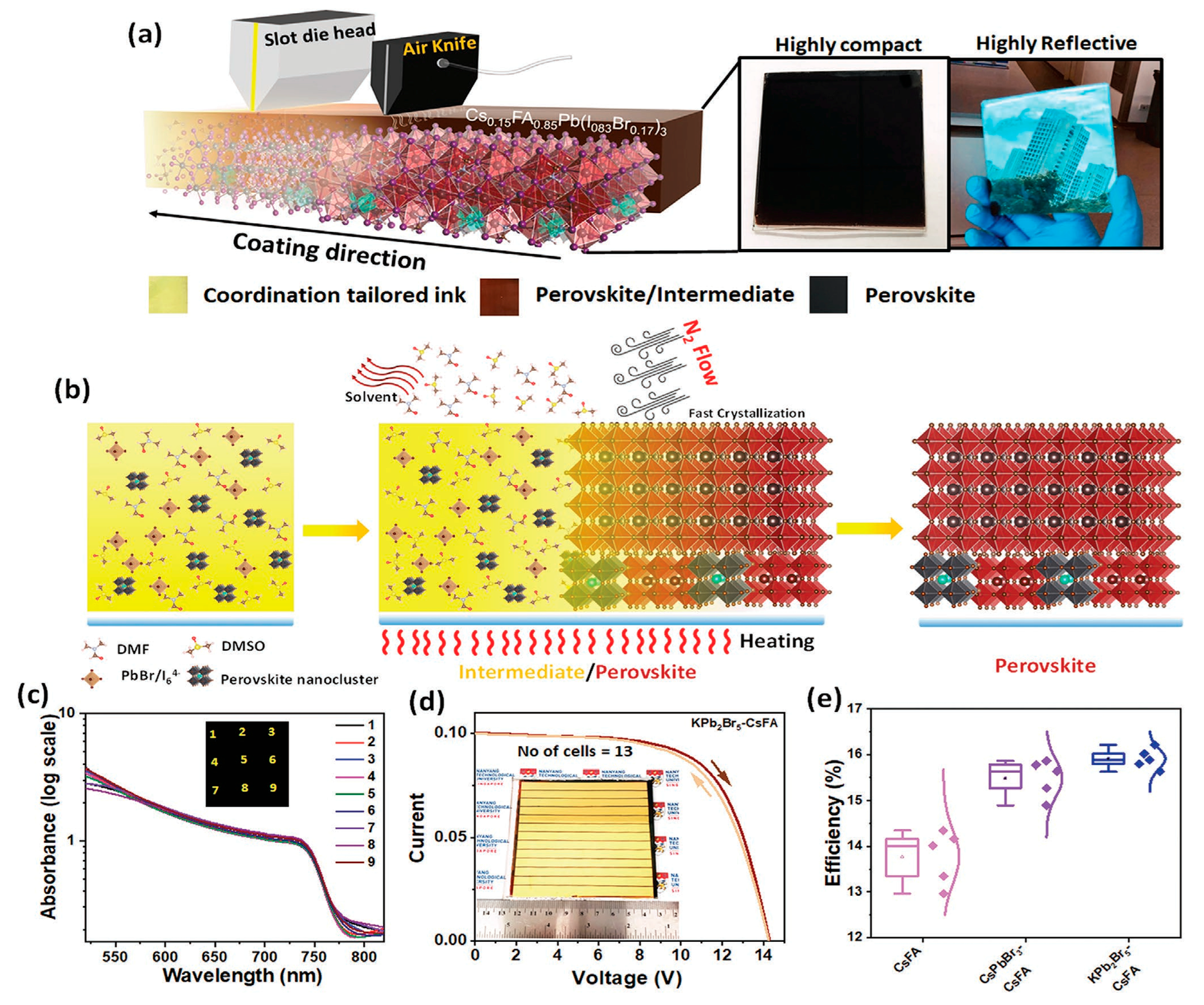
4.3. Slot-Die Coating
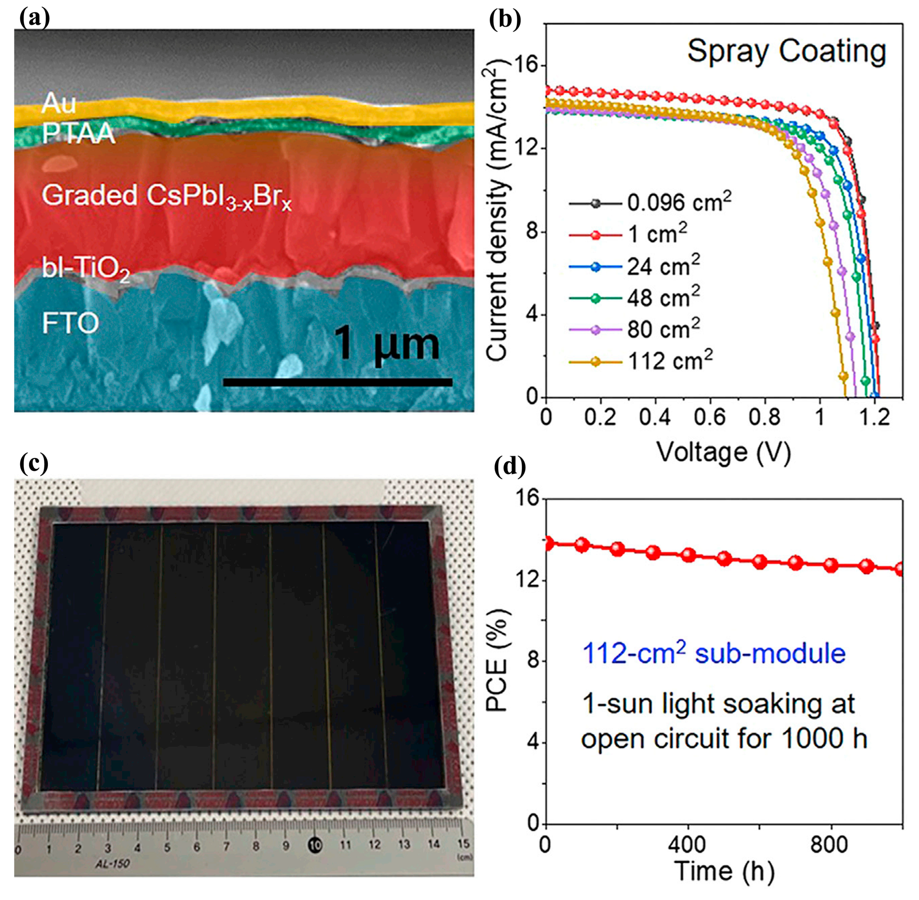
4.4. Spray-Coating
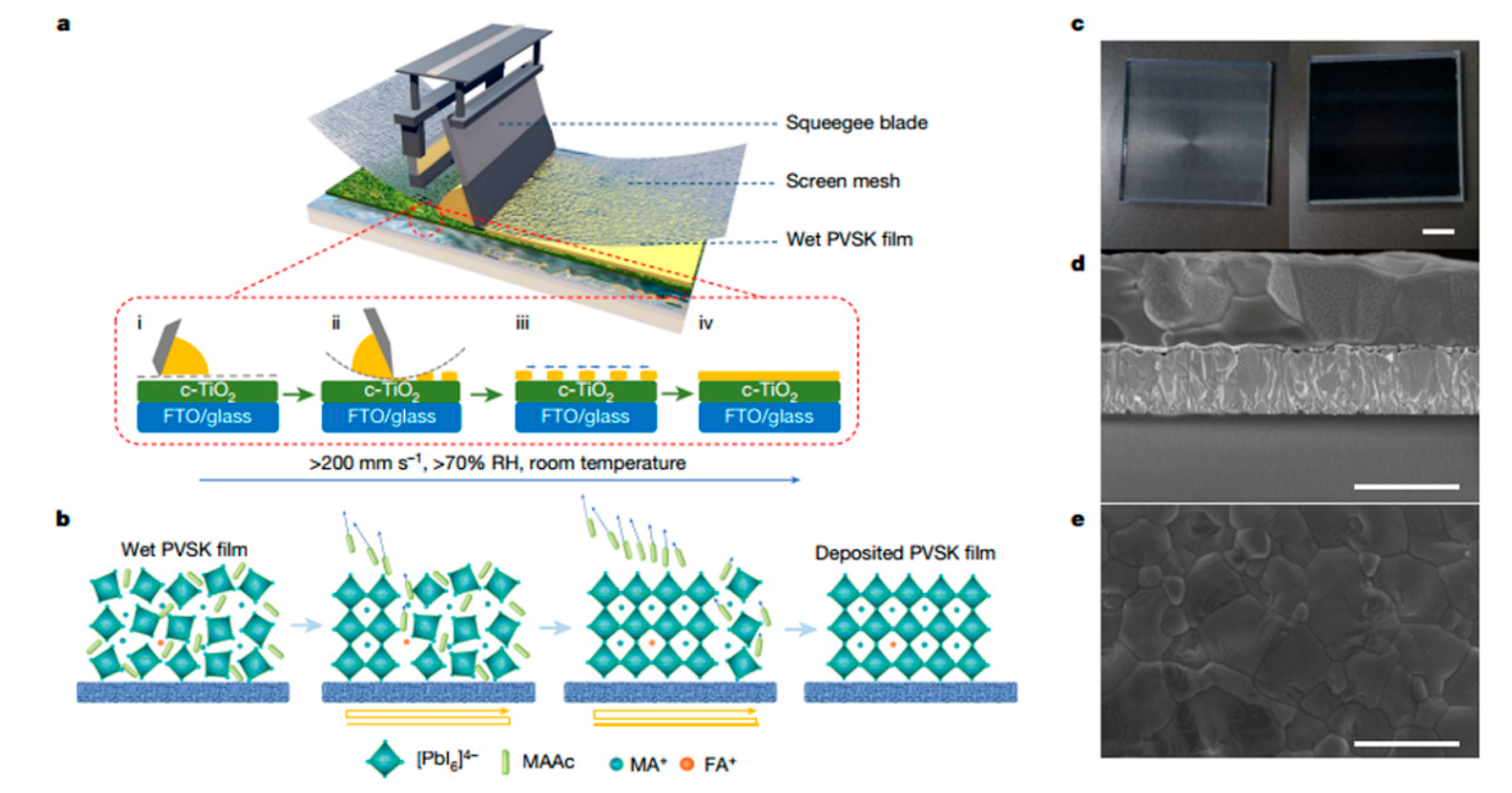
4.5. Screen Printing
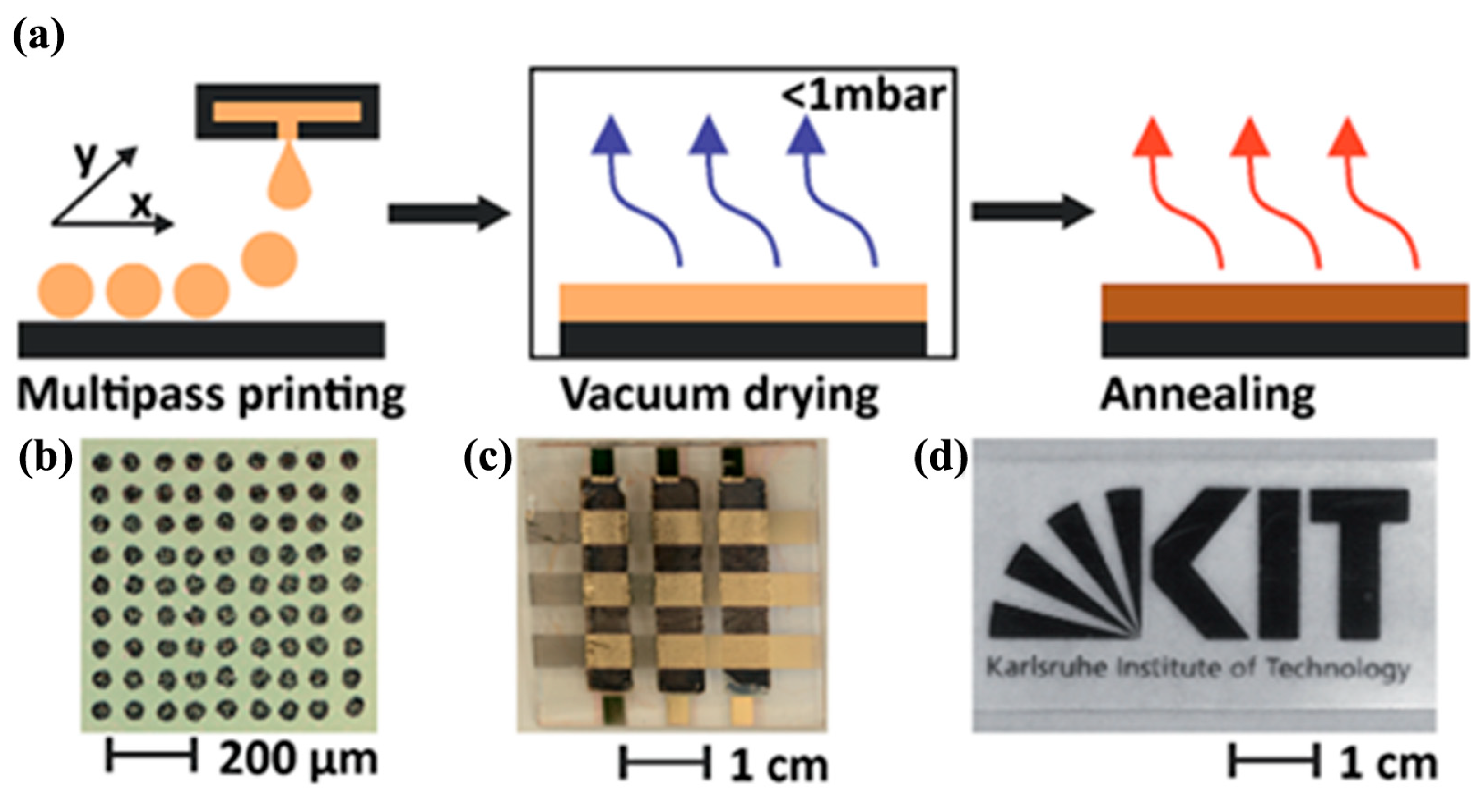
4.6. Inkjet Printing
5. Summary and Perspectives
Supplementary Materials
Author Contributions
Funding
Data Availability Statement
Conflicts of Interest
References
- Sun, M.; Liu, X.; Zhang, F.; Liu, H.; Liu, X.; Wang, S.; Xiao, Y.; Li, D.; Meng, Q.; Li, X. Simple dopant-free hole-transporting materials with p-π conjugated structure for stable perovskite solar cells. Appl. Surf. Sci. 2017, 416, 124–132. [Google Scholar] [CrossRef]
- Sun, M.; Wang, S.; Xiao, Y.; Song, Z.; Li, X. Titanylphthalocyanine as hole transporting material for perovskite solar cells. J. Energy Chem. 2015, 24, 756–761. [Google Scholar] [CrossRef]
- Kojima, A.; Teshima, K.; Shirai, Y.; Miyasaka, T. Organometal halide perovskites as visible-light sensitizers for photovoltaic Cells. J. Am. Chem. Soc. 2009, 131, 6050–6051. [Google Scholar] [CrossRef] [PubMed]
- Sun, M.; Zhang, F.; Liu, H.; Li, X.; Xiao, Y.; Wang, S. Tuning the crystal growth of perovskite thin-films by adding the 2-pyridylthiourea additive for highly efficient and stable solar cells prepared in ambient air. J. Mater. Chem. A 2017, 5, 13448–13456. [Google Scholar] [CrossRef]
- Kim, H.-S.; Lee, C.-R.; Im, J.-H.; Lee, K.-B.; Moehl, T.; Marchioro, A.; Moon, S.-J.; Humphry-Baker, R.; Yum, J.-H.; Moser, J.E.; et al. Lead iodide perovskite sensitized all-solid-state submicron thin film mesoscopic solar cell with efficiency exceeding 9%. Sci. Rep. 2012, 2, 591. [Google Scholar] [CrossRef]
- Liu, L.; Wang, Z.; Sun, W.; Zhang, J.; Hu, S.; Hayat, T.; Alsaedi, A.; Tan, Z.A. All-solution-processed perovskite light-emitting diodes with all metal oxide transport layers. Chem. Commun. 2018, 54, 13283–13286. [Google Scholar] [CrossRef]
- Zhou, Q.; Bai, Z.; Lu, W.-g.; Wang, Y.; Zou, B.; Zhong, H. In situ fabrication of halide perovskite nanocrystal-embedded polymer composite films with enhanced photoluminescence for display backlights. Adv. Mater. 2016, 28, 9163–9168. [Google Scholar] [CrossRef]
- Han, T.-H.; Choi, M.-R.; Woo, S.-H.; Min, S.-Y.; Lee, C.-L.; Lee, T.-W. Molecularly controlled interfacial layer strategy toward highly efficient simple-structured organic light-emitting diodes. Adv. Mater. 2012, 24, 1487–1493. [Google Scholar] [CrossRef]
- Sun, M.; Zhang, F.; Luo, X.; Zhang, D.; Duan, L. Mixed 2D/3D perovskite with fine phase control modulated by a novel cyclopentanamine hydrobromide for better stability in light-emitting diodes. Chem. Eng. J. 2020, 393, 124787. [Google Scholar] [CrossRef]
- Deschler, F.; Price, M.; Pathak, S.; Klintberg, L.E.; Jarausch, D.-D.; Higler, R.; Hüttner, S.; Leijtens, T.; Stranks, S.D.; Snaith, H.J.; et al. High photoluminescence efficiency and optically pumped lasing in solution-processed mixed halide perovskite semiconductors. J. Phys. Chem. Lett. 2014, 5, 1421–1426. [Google Scholar] [CrossRef]
- Sun, M.; Kang, L.; Jiao, Z.; Yuan, G.; Huang, Q.; Wang, P.; Li, Y.; Liu, X. Enhancement performance of vapor-deposition processed perovskite photodetectors enabled by manipulation of interface engineering. Org. Electron. 2023, 116, 106773. [Google Scholar] [CrossRef]
- Chen, H.-W.; Sakai, N.; Jena, A.K.; Sanehira, Y.; Ikegami, M.; Ho, K.-C.; Miyasaka, T. A Switchable high-sensitivity photodetecting and photovoltaic device with perovskite absorber. J. Phys. Chem. Lett. 2015, 6, 1773–1779. [Google Scholar] [CrossRef] [PubMed]
- Liu, C.; Yang, Y.; Chen, H.; Spanopoulos, I.; Bati, A.S.R.; Gilley, I.W.; Chen, J.; Maxwell, A.; Vishal, B.; Reynolds, R.P.; et al. Two-dimensional perovskitoids enhance stability in perovskite solar cells. Nature 2024, 633, 359–364. [Google Scholar] [CrossRef]
- Liang, Z.; Zhang, Y.; Xu, H.; Chen, W.; Liu, B.; Zhang, J.; Zhang, H.; Wang, Z.; Kang, D.-H.; Zeng, J.; et al. Homogenizing out-of-plane cation composition in perovskite solar cells. Nature 2023, 624, 557–563. [Google Scholar] [CrossRef]
- Kim, J.Y.; Lee, J.-W.; Jung, H.S.; Shin, H.; Park, N.-G. High-efficiency perovskite solar cells. Chem. Rev. 2020, 120, 7867–7918. [Google Scholar] [CrossRef]
- Ma, C.; Kang, M.-C.; Lee, S.-H.; Zhang, Y.; Kang, D.-H.; Yang, W.; Zhao, P.; Kim, S.-W.; Kwon, S.J.; Yang, C.-W.; et al. Facet-dependent passivation for efficient perovskite solar cells. J. Am. Chem. Soc. 2023, 145, 24349–24357. [Google Scholar] [CrossRef]
- Ma, F.; Zhao, Y.; Qu, Z.; You, J. Developments of highly efficient perovskite solar cells. Acc. Mater. Res. 2023, 4, 716–725. [Google Scholar] [CrossRef]
- Wang, K.; Zheng, L.; Zhu, T.; Yao, X.; Yi, C.; Zhang, X.; Cao, Y.; Liu, L.; Hu, W.; Gong, X. Efficient perovskite solar cells by hybrid perovskites incorporated with heterovalent neodymium cations. Nano Energy 2019, 61, 352–360. [Google Scholar] [CrossRef]
- Yang, X.; Li, Q.; Zheng, Y.; Luo, D.; Zhang, Y.; Tu, Y.; Zhao, L.; Wang, Y.; Xu, F.; Gong, Q.; et al. Perovskite hetero-bilayer for efficient charge-transport-layer-free solar cells. Joule 2022, 6, 1277–1289. [Google Scholar] [CrossRef]
- Yang, W.; Yao, Y.; Wu, C.-Q. Mechanism of charge recombination in meso-structured organic-inorganic hybrid perovskite solar cells: A macroscopic perspective. J. Appl. Phys. 2015, 117, 155504. [Google Scholar] [CrossRef]
- Seo, J.; Noh, J.H.; Seok, S.I. Rational strategies for efficient perovskite solar cells. Acc. Chem. Res. 2016, 49, 562–572. [Google Scholar] [CrossRef] [PubMed]
- Zhou, J.; Tan, L.; Liu, Y.; Li, H.; Liu, X.; Li, M.; Wang, S.; Zhang, Y.; Jiang, C.; Hua, R.; et al. Highly efficient and stable perovskite solar cells via a multifunctional hole transporting material. Joule 2024, 8, 1691–1706. [Google Scholar] [CrossRef]
- Liu, C.; Yang, Y.; Chen, H.; Xu, J.; Liu, A.; Bati, A.S.R.; Zhu, H.; Grater, L.; Hadke, S.S.; Huang, C.; et al. Bimolecularly passivated interface enables efficient and stable inverted perovskite solar cells. Science 2023, 382, 810–815. [Google Scholar] [CrossRef] [PubMed]
- Miyata, A.; Mitioglu, A.; Plochocka, P.; Portugall, O.; Wang, J.T.-W.; Stranks, S.D.; Snaith, H.J.; Nicholas, R.J. Direct measurement of the exciton binding energy and effective masses for charge carriers in organic-inorganic tri-halide perovskites. Nat. Phys. 2015, 11, 582–587. [Google Scholar] [CrossRef]
- Correa-Baena, J.-P.; Luo, Y.; Brenner, T.M.; Snaider, J.; Sun, S.; Li, X.; Jensen, M.A.; Hartono, N.T.P.; Nienhaus, L.; Wieghold, S.; et al. Homogenized halides and alkali cation segregation in alloyed organic-inorganic perovskites. Science 2019, 363, 627–631. [Google Scholar] [CrossRef]
- Hambsch, M.; Lin, Q.; Armin, A.; Burn, P.L.; Meredith, P. Efficient, monolithic large area organohalide perovskite solar cells. J. Mater. Chem. A 2016, 4, 13830–13836. [Google Scholar] [CrossRef]
- Rana, N.K.; Das, T.; Garg, P.; Bera, A.; Guchhait, A. PTAA/Ag-based large area perovskite solar cells toward low-cost and ambient stability. J. Phys. Chem. C 2023, 127, 21954–21962. [Google Scholar] [CrossRef]
- Tomulescu, A.G.; Stancu, V.; Beşleagă, C.; Enculescu, M.; Nemneş, G.A.; Florea, M.; Dumitru, V.; Pintilie, L.; Pintilie, I.; Leonat, L. Reticulated mesoporous TiO2 scaffold, fabricated by spray coating for large-area perovskite solar cells. Energy Technol. 2020, 8, 1900922. [Google Scholar] [CrossRef]
- Jiang, C.; Lim, S.L.; Goh, W.P.; Wei, F.X.; Zhang, J. Improvement of CH3NH3PbI3 Formation for efficient and better reproducible mesoscopic perovskite solar cells. ACS Appl. Mater. Interfaces 2015, 44, 24726–24732. [Google Scholar] [CrossRef]
- Wei, M.; Xiao, K.; Walters, G.; Lin, R.; Zhao, Y.; Saidaminov, M.I.; Todorović, P.; Johnston, A.; Huang, Z.; Chen, H.; et al. Combining efficiency and stability in mixed Tin-lead perovskite solar cells by capping grains with an ultrathin 2D layer. Adv. Mater. 2020, 32, 1907058. [Google Scholar] [CrossRef]
- Zhu, H.; Liu, Y.; Eickemeyer, F.T.; Pan, L.; Ren, D.; Ruiz-Preciado, M.A.; Carlsen, B.; Yang, B.; Dong, X.; Wang, Z.; et al. Tailored amphiphilic molecular mitigators for stable perovskite solar cells with 23.5% Efficiency. Adv. Mater. 2020, 32, 1907757. [Google Scholar] [CrossRef] [PubMed]
- Park, M.; Cho, W.; Lee, G.; Hong, S.C.; Kim, M.-c.; Yoon, J.; Ahn, N.; Choi, M. Highly reproducible large-area perovskite solar cell fabrication via continuous megasonic spray coating of CH3NH3PbI3. Small 2019, 15, 1804005. [Google Scholar] [CrossRef]
- Lee, H.J.; Park, J.K.; Heo, J.H.; Im, S.H. Acetylacetone-TiO2 promoted large area compatible cascade electron transport bilayer for efficient perovskite solar cells. Energy Environ. Mater. 2024, 7, e12582. [Google Scholar] [CrossRef]
- Huang, S.-H.; Guan, C.K.; Lee, P.H.; Huang, H.C.; Li, C.-F.; Huang, Y.C.; Su, W. Toward all slot-die fabricated high efficiency large area perovskite solar cell using rapid near infrared heating in ambient air. Adv. Energy Mater. 2020, 10, 2001567. [Google Scholar] [CrossRef]
- Wang, L.; Zhang, T.; Yuan, S.; Qian, F.; Li, X.; Zheng, H.; Huang, J.; Li, S. Over 19% Efficiency perovskite solar modules by simultaneously suppressing cation deprotonation and iodide oxidation. ACS Appl. Mater. Interfaces. 2024, 16, 4751–4762. [Google Scholar] [CrossRef]
- Taheri, B.; Calabrò, E.; Matteocci, F.; Di Girolamo, D.; Cardone, G.; Liscio, A.; Di Carlo, A.; Brunetti, F. Automated scalable spray coating of SnO2 for the fabrication of low-temperature perovskite solar cells and modules. Energy Technol. 2020, 8, 1901284. [Google Scholar] [CrossRef]
- Wang, K.; Du, Y.; Liang, J.; Zhao, J.; Xu, F.F.; Liu, X.; Zhang, C.; Yan, Y.; Zhao, Y.S. Wettability-guided screen printing of perovskite microlaser arrays for current-driven displays. Adv. Mater. 2020, 32, 2001999. [Google Scholar] [CrossRef]
- Wang, X.; Fang, J.; Li, S.; Xie, G.; Lin, D.; Li, H.; Wang, D.; Huang, N.; Peng, H.; Qiu, L. Lead iodide redistribution enables in situ passivation for blading inverted perovskite solar cells with 24.5% efficiency. Small 2024, 20, 2404058. [Google Scholar] [CrossRef]
- Huang, C.; Tan, S.; Yu, B.; Li, Y.; Shi, J.; Wu, H.; Luo, Y.; Li, D.; Meng, Q. Meniscus-modulated blade coating enables high-quality a-phase formamidinium lead triiodide crystals and efficient perovskite minimodules. Joule 2024, 8, 2539–2553. [Google Scholar] [CrossRef]
- Wang, L.; Zheng, D.; Li, Z.; Farhadi, B.; Peng, L.; Zhao, S.; Chang, Z.; Duan, L.; Cao, Y.; Wang, H.; et al. Surfactant engineering for perovskite solar cells and submodules. Matter 2023, 6, 2987–3005. [Google Scholar] [CrossRef]
- Bu, T.; Li, J.; Li, H.; Tian, C.; Su, J.; Tong, G.; Ono, L.K.; Wang, C.; Lin, Z.; Chai, N.; et al. Lead halide-templated crystallization of methylamine-free perovskite for efficient photovoltaic modules. Science 2021, 372, 1327–1332. [Google Scholar] [CrossRef] [PubMed]
- Parida, B.; Singh, A.; Kalathil Soopy, A.K.; Sangaraju, S.; Sundaray, M.; Mishra, S.; Liu, S.; Najar, A. Recent developments in upscalable printing techniques for perovskite solar cells. Adv. Sci. 2022, 9, 2200308. [Google Scholar] [CrossRef] [PubMed]
- Hu, Y.; Chu, Y.; Wang, Q.; Zhang, Z.; Ming, Y.; Mei, A.; Rong, Y.; Han, H. Standardizing perovskite solar modules beyond cells. Joule 2019, 3, 2076–2085. [Google Scholar] [CrossRef]
- Wang, G.; Adil, M.A.; Zhang, J.; Wei, Z. Large-area organic solar cells: Material requirements, modular designs, and printing methods. Adv. Mater. 2019, 31, 1805089. [Google Scholar] [CrossRef]
- Wu, Z.; Sang, S.; Zheng, J.; Gao, Q.; Huang, B.; Li, F.; Sun, K.; Chen, S. Crystallization kinetics of hybrid perovskite solar cells. Angew. Chem. Int. Edit. 2024, 63, e202319170. [Google Scholar] [CrossRef]
- Ma, S.; Sansoni, S.; Gatti, T.; Fino, P.; Liu, G.; Lamberti, F. Research progress on homogeneous fabrication of large-area perovskite films by spray coating. Crystals 2023, 13, 216. [Google Scholar] [CrossRef]
- Xie, Y.-M.; Xue, Q.; Yip, H.-L. Metal-halide perovskite crystallization kinetics: A review of experimental and theoretical studies. Adv. Energy Mater. 2021, 11, 2100784. [Google Scholar] [CrossRef]
- Wang, Z.; Duan, X.; Zhang, J.; Yuan, W.; Qu, D.; Chen, Y.; He, L.; Wang, H.; Yang, G.; Zhang, W.; et al. Manipulating the crystallization kinetics of halide perovskites for large-area solar modules. Commun. Mater. 2024, 5, 131. [Google Scholar] [CrossRef]
- Zhu, P.; Chen, C.; Dai, J.; Zhang, Y.; Mao, R.; Chen, S.; Huang, J.; Zhu, J. Toward the commercialization of perovskite solar modules. Adv. Mater. 2024, 36, 2307357. [Google Scholar] [CrossRef]
- Lee, J.-W.; Lee, D.-K.; Jeong, D.-N.; Park, N.-G. Control of Crystal Growth toward scalable fabrication of perovskite solar cells. Adv. Fun. Mater. 2019, 29, 1807047. [Google Scholar] [CrossRef]
- Li, Z.; Klein, T.R.; Kim, D.H.; Yang, M.; Berry, J.J.; van Hest, M.F.A.M.; Zhu, K. Scalable fabrication of perovskite solar cells. Nat. Rev. Mater. 2018, 3, 18017. [Google Scholar]
- Chen, Z.; He, P.; Wu, D.; Chen, C.; Mujahid, M.; Li, Y.; Duan, Y. Processing and preparation method for high-quality opto-electronic perovskite film. Front. Mater. 2021, 8, 723169. [Google Scholar] [CrossRef]
- Xiao, M.; Huang, F.; Huang, W.; Dkhissi, Y.; Zhu, Y.; Etheridge, J.; Gray-Weale, A.; Bach, U.; Cheng, Y.-B.; Spiccia, L. A fast deposition-crystallization procedure for highly efficient lead iodide perovskite thin-film solar cells. Angew. Chem. Int. Edit. 2014, 53, 9898–9903. [Google Scholar] [CrossRef]
- Yang, W.S.; Noh, J.H.; Jeon, N.J.; Kim, Y.C.; Ryu, S.; Seo, J.; Seok, S.I. High-performance photovoltaic perovskite layers fabricated through intramolecular exchange. Science 2015, 348, 1234–1237. [Google Scholar] [CrossRef]
- Guo, Y.; Sato, W.; Shoyama, K.; Nakamura, E. Sulfamic acid-catalyzed lead perovskite formation for solar cell fabrication on glass or plastic substrates. J. Am. Chem. Soc. 2016, 138, 5410–5416. [Google Scholar] [CrossRef]
- Sahli, F.; Werner, J.; Kamino, B.A.; Bräuninger, M.; Monnard, R.; Paviet-Salomon, B.; Barraud, L.; Ding, L.; Diaz Leon, J.J.; Sacchetto, D.; et al. Fully textured monolithic perovskite/silicon tandem solar cells with 25.2% power conversion efficiency. Nat. Mater 2018, 17, 820–826. [Google Scholar] [CrossRef]
- Jiang, Q.; Zhao, Y.; Zhang, X.; Yang, X.; Chen, Y.; Chu, Z.; Ye, Q.; Li, X.; Yin, Z.; You, J. Surface passivation of perovskite film for efficient solar cells. Nat. Photonics 2019, 13, 460–466. [Google Scholar] [CrossRef]
- Kim, D.H.; Muzzillo, C.P.; Tong, J.; Palmstrom, A.F.; Larson, B.W.; Choi, C.; Harvey, S.P.; Glynn, S.; Whitaker, J.B.; Zhang, F.; et al. Bimolecular additives improve wide-band-gap perovskites for efficient tandem solar cells with CIGS. Joule 2019, 3, 1734–1745. [Google Scholar] [CrossRef]
- Jeong, J.; Kim, M.; Seo, J.; Lu, H.; Ahlawat, P.; Mishra, A.; Yang, Y.; Hope, M.A.; Eickemeyer, F.T.; Kim, M.; et al. Pseudo-halide anion engineering for α-FAPbI3 perovskite solar cells. Nature 2021, 592, 381–3855. [Google Scholar] [CrossRef]
- Kim, J.; Yun, J.S.; Cho, Y.; Lee, D.S.; Wilkinson, B.; Soufiani, A.M.; Deng, X.; Zheng, J.; Shi, A.; Lim, S.; et al. Overcoming the challenges of large-area high-efficiency perovskite solar cells. ACS Energy Lett. 2017, 2, 1978–1984. [Google Scholar] [CrossRef]
- Yang, Z.; Chueh, C.-C.; Zuo, F.; Kim, J.H.; Liang, P.-W.; Jen, A.K.Y. High-performance fully printable perovskite solar cells via blade-coating technique under the ambient condition. Adv. Energy Mater. 2015, 5, 1500328. [Google Scholar] [CrossRef]
- Li, C.; Yin, J.; Chen, R.; Lv, X.; Feng, X.; Wu, Y.; Cao, J. Monoammonium porphyrin for blade-coating stable large-area perovskite solar cells with >18% efficiency. J. Am. Chem. Soc. 2019, 141, 6345–6351. [Google Scholar] [CrossRef]
- Tang, S.; Deng, Y.; Zheng, X.; Bai, Y.; Fang, Y.; Dong, Q.; Wei, H.; Huang, J. Composition engineering in doctor-blading of perovskite solar cells. Adv. Energy Mater. 2017, 7, 1700302. [Google Scholar] [CrossRef]
- Li, J.; Munir, R.; Fan, Y.; Niu, T.; Liu, Y.; Zhong, Y.; Yang, Z.; Tian, Y.; Liu, B.; Sun, J.; et al. Phase transition control for high-performance blade-coated perovskite solar cells. Joule 2018, 2, 1313–1330. [Google Scholar] [CrossRef]
- Huang, S.-H.; Tian, K.-Y.; Huang, H.-C.; Li, C.-F.; Chu, W.-C.; Lee, K.-M.; Huang, Y.-C.; Su, W.-F. Controlling the morphology and interface of the perovskite layer for scalable high-efficiency solar cells fabricated using green solvents and blade coating in an ambient environment. ACS Appl. Mater. Interfaces 2020, 12, 26041–26049. [Google Scholar] [CrossRef]
- Zhao, X.; Zhang, P.; Liu, T.; Tian, B.; Jiang, Y.; Zhang, J.; Tang, Y.; Li, B.; Xue, M.; Zhang, W.; et al. Operationally stable perovskite solar modules enabled by vapor-phase fluoride treatment. Science 2024, 385, 433–438. [Google Scholar] [CrossRef]
- Fievez, M.; Singh Rana, P.J.; Koh, T.M.; Manceau, M.; Lew, J.H.; Jamaludin, N.F.; Ghosh, B.; Bruno, A.; Cros, S.; Berson, S.; et al. Slot-die coated methylammonium-free perovskite solar cells with 18% efficiency. Sol. Energ. Mat. Sol. C 2021, 230, 111189. [Google Scholar] [CrossRef]
- Du, M.; Zhu, X.; Wang, L.; Wang, H.; Feng, J.; Jiang, X.; Cao, Y.; Sun, Y.; Duan, L.; Jiao, Y.; et al. High-pressure nitrogen-extraction and effective passivation to attain highest large-area perovskite solar module efficiency. Adv. Mater. 2020, 32, 2004979. [Google Scholar] [CrossRef]
- Rana, P.J.S.; Febriansyah, B.; Koh, T.M.; Muhammad, B.T.; Salim, T.; Hooper, T.J.N.; Kanwat, A.; Ghosh, B.; Kajal, P.; Lew, J.H.; et al. Alkali Additives enable efficient large area (>55 cm2) slot-die coated perovskite solar modules. Adv. Fun. Mater. 2022, 32, 2113026. [Google Scholar] [CrossRef]
- Zimmermann, I.; Al Atem, M.; Fournier, O.; Bernard, S.; Jutteau, S.; Lombez, L.; Rousset, J. Sequentially Slot-die-coated perovskite for efficient and scalable solar cells. Adv. Mater. Interfaces 2021, 8, 2100743. [Google Scholar] [CrossRef]
- Li, J.; Dagar, J.; Shargaieva, O.; Maus, O.; Remec, M.; Emery, Q.; Khenkin, M.; Ulbrich, C.; Akhundova, F.; Márquez, J.A.; et al. Ink design enabling slot-die coated perovskite solar cells with >22% power conversion efficiency, micro-modules, and 1 year of outdoor performance evaluation. Adv. Energy Mater. 2023, 13, 2203898. [Google Scholar] [CrossRef]
- Barrows, A.T.; Pearson, A.J.; Kwak, C.K.; Dunbar, A.D.F.; Buckley, A.R.; Lidzey, D.G. Efficient planar heterojunction mixed-halide perovskite solar cells deposited via spray-deposition. Energy Environ. Sci. 2014, 7, 2944–2950. [Google Scholar] [CrossRef]
- Chou, L.-H.; Wang, X.-F.; Osaka, I.; Wu, C.-G.; Liu, C.-L. Scalable ultrasonic spray-processing technique for manufacturing large-area CH3NH3PbI3 perovskite solar cells. ACS Appl. Mater. Interfaces 2018, 10, 38042–38050. [Google Scholar] [CrossRef]
- Jiang, Y.; Remeika, M.; Hu, Z.; Juarez-Perez, E.J.; Qiu, L.; Liu, Z.; Kim, T.; Ono, L.K.; Son, D.-Y.; Hawash, Z.; et al. Negligible-Pb-waste and upscalable perovskite deposition technology for high-operational-stability perovskite solar modules. Adv. Energy Mater. 2019, 9, 1803047. [Google Scholar] [CrossRef]
- Cai, H.; Liang, X.; Ye, X.; Su, J.; Guan, J.; Yang, J.; Liu, Y.; Zhou, X.; Han, R.; Ni, J.; et al. High efficiency over 20% of perovskite solar cells by spray coating via a simple process. ACS Appl. Energy Mater. 2020, 3, 9696–9702. [Google Scholar] [CrossRef]
- Heo, J.H.; Zhang, F.; Xiao, C.; Heo, S.J.; Park, J.K.; Berry, J.J.; Zhu, K.; Im, S.H. Efficient and stable graded CsPbI3-xBrx perovskite solar cells and submodules by orthogonal processable spray coating. Joule 2021, 5, 481–494. [Google Scholar] [CrossRef]
- Yu, X.; Mo, Y.; Li, J.; Ku, Z.; Xiao, J.; Long, F.; Han, L.; Li, W.; Lei, S.; Peng, Y.; et al. Moisture control enables high-performance sprayed perovskite solar cells under ambient conditions. Mater. Today Energy 2023, 37, 101391. [Google Scholar] [CrossRef]
- Chen, C.; Ran, C.; Guo, C.; Yao, Q.; Wang, J.; Niu, T.; Li, D.; Chao, L.; Xia, Y.; Chen, Y. Fully screen-printed perovskite solar cells with 17% Efficiency via tailoring confined perovskite crystallization within mesoporous layer. Adv. Energy Mater. 2023, 13, 2302654. [Google Scholar] [CrossRef]
- Mishra, A.; Ahmad, Z.; Zimmermann, I.; Martineau, D.; Shakoor, R.A.; Touati, F.; Riaz, K.; Al-Muhtaseb, S.A.; Nazeeruddin, M.K. Effect of annealing temperature on the performance of printable carbon electrodes for perovskite solar cells. Organ. Electron. 2019, 65, 375–380. [Google Scholar] [CrossRef]
- De Rossi, F.; Baker, J.A.; Beynon, D.; Hooper, K.E.A.; Meroni, S.M.P.; Williams, D.; Wei, Z.; Yasin, A.; Charbonneau, C.; Jewell, E.H.; et al. All printable perovskite solar modules with 198 cm2 active area and over 6% efficiency. Adv. Mater. Technol. 2018, 3, 1800156. [Google Scholar] [CrossRef]
- Vanessa, M. Preparation of highly efficient carbon-based perovskite solar cells (C-based PSCs) by screen-printing. In Organic, Hybrid, and Perovskite Photovoltaics XX; SPIE: Bellingham, WA, USA, 2019; Volume 11094, pp. 37–42. [Google Scholar]
- Cao, K.; Zuo, Z.; Cui, J.; Shen, Y.; Moehl, T.; Zakeeruddin, S.M.; Grätzel, M.; Wang, M. Efficient screen printed perovskite solar cells based on mesoscopic TiO2/Al2O3/NiO/carbon architecture. Nano Energy 2015, 17, 171–179. [Google Scholar] [CrossRef]
- De Rossi, F.; Barbé, J.; Tanenbaum, D.M.; Cinà, L.; Castriotta, L.A.; Stoichkov, V.; Wei, Z.; Tsoi, W.C.; Kettle, J.; Sadula, A.; et al. An interlaboratory study on the stability of all-printable hole transport material–free perovskite solar cells. Energy Technol. 2020, 8, 2000134. [Google Scholar] [CrossRef]
- Mei, A.; Li, X.; Liu, L.; Ku, Z.; Liu, T.; Rong, Y.; Xu, M.; Hu, M.; Chen, J.; Yang, Y.; et al. A hole-conductor-free, fully printable mesoscopic perovskite solar cell with high stability. Science 2014, 345, 295–298. [Google Scholar] [CrossRef]
- Chen, C.; Chen, J.; Han, H.; Chao, L.; Hu, J.; Niu, T.; Dong, H.; Yang, S.; Xia, Y.; Chen, Y.; et al. Perovskite solar cells based on screen-printed thin films. Nature 2022, 612, 266–271. [Google Scholar] [CrossRef]
- He, J.; He, J.; Ma, D.; Shao, W.; Sheng, J.; Zhang, H.; Zhang, L.; Zou, C.; Ding, T.; Cen, R.; et al. Implementing a two-in-one defect passivation strategy utilizing CsX for high-performance printable carbon-based perovskite solar cells. Adv. Fun. Mater. 2024, 34, 2405986. [Google Scholar] [CrossRef]
- Wei, Z.; Chen, H.; Yan, K.; Yang, S. Inkjet printing and instant chemical transformation of a CH3NH3PbI3/nanocarbon electrode and interface for planar perovskite solar cells. Angew. Chem. Int. Edit. 2014, 53, 13239–13243. [Google Scholar] [CrossRef]
- Mathies, F.; Abzieher, T.; Hochstuhl, A.; Glaser, K.; Colsmann, A.; Paetzold, U.W.; Hernandez-Sosa, G.; Lemmer, U.; Quintilla, A. Multipass inkjet printed planar methylammonium lead iodide perovskite solar cells. J. Mater. Chem. A 2016, 4, 19207–19213. [Google Scholar] [CrossRef]
- Li, P.; Liang, C.; Bao, B.; Li, Y.; Hu, X.; Wang, Y.; Zhang, Y.; Li, F.; Shao, G.; Song, Y. Inkjet manipulated homogeneous large size perovskite grains for efficient and large-area perovskite solar cells. Nano Energy 2018, 46, 203–211. [Google Scholar] [CrossRef]
- Huckaba, A.J.; Lee, Y.; Xia, R.; Paek, S.; Bassetto, V.C.; Oveisi, E.; Lesch, A.; Kinge, S.; Dyson, P.J.; Girault, H.; et al. Inkjet-printed mesoporous TiO2 and perovskite layers for high efficiency perovskite solar cells. Energy Technol. 2019, 7, 317–324. [Google Scholar] [CrossRef]
- Schackmar, F.; Eggers, H.; Frericks, M.; Richards, B.S.; Lemmer, U.; Hernandez-Sosa, G.; Paetzold, U.W. Perovskite solar cells with all-inkjet-printed absorber and charge transport layers. Adv. Mater. Technol. 2021, 6, 2000271. [Google Scholar] [CrossRef]
- Tan, L.; Jiang, H.; Yang, R.; Shen, L.; Sun, C.; Jin, Y.; Guan, X.; Song, P.; Zheng, L.; Tian, C.; et al. Quantitative surface passivation through drop-on-demand inkjet printing enables highly efficient perovskite solar cells. Adv. Energy Mater. 2024, 14, 2400549. [Google Scholar] [CrossRef]
- Kang, B.; Yan, F. Emerging strategies for the large-scale fabrication of perovskite solar modules: From design to process. Energy Environ. Sci. 2025. [Google Scholar] [CrossRef]
- Green, M.A.; Dunlop, E.D.; Yoshita, M.; Kopidakis, N.; Bothe, K.; Siefer, G.; Hinken, D.; Rauer, M.; Hohl-Ebinger, J.; Hao, X. Solar cell efficiency tables (version 57). Prog. Photovolt. Res. Appl. 2024, 32, 425–441. [Google Scholar] [CrossRef]
- Li, J.; Fan, B.; Liu, X.; Liu, Y.; Xing, Z.; Gong, C.; Chu, Z.; Li, L.; Meng, X.; Guo, R.; et al. Polymer modulated ink rheology and compatibility enables homogenized printing of a Spiro-OMeTAD transport layer for scalable and stable perovskite solar modules. Energy Environ. Sci. 2024, 17, 6821–6832. [Google Scholar] [CrossRef]
- Du, M.; Zhao, S.; Duan, L.; Cao, Y.; Wang, H.; Sun, Y.; Wang, L.; Zhu, X.; Feng, J.; Liu, L.; et al. Surface redox engineering of vacuum-deposited NiOx for top-performance perovskite solar cells and modules. Joule 2022, 6, 1931–1943. [Google Scholar] [CrossRef]
- Xu, T.; Li, Y.; Cai, H.; Zhu, Y.; Liu, C.; Han, B.; Hu, Z.; Zhang, F.; Ni, J.; Li, J.; et al. Co-solvent strategy for highly efficient perovskite solar cells by spray coating. Solar Energy 2024, 272, 112461. [Google Scholar] [CrossRef]
- Zhao, J.; Yang, X.; Zhou, W.; Wang, R.; Wang, Y.; Zhang, J.; Zhong, X.; Ren, H.; Hou, G.; Ding, Y.; et al. Performance amelioration of spray-coated perovskite solar cells utilizing a self-assembled monolayer. ACS Appl. Energy Mater 2024, 7, 3540–3549. [Google Scholar] [CrossRef]
- Pai, N.; Angmo, D. Powering the future: Opportunities and obstacles in lead-halide inorganic perovskite solar cells. Adv. Sci. 2025, 12, 2412666. [Google Scholar] [CrossRef]
- Tsvetkov, N.; Lee, M.; Kim, Y.; Kim, D.; Yun, J.S.; Min, H. Advancements in Perovskite Solar Cell Concentrators and Future Prospects. J. Mater. Chem. A 2025, 13, 7656–7681. [Google Scholar] [CrossRef]
- Yuan, S.; Zheng, D.; Zhang, T.; Wang, Y.; Qian, F.; Wang, L.; Li, X.; Zheng, H.; Diao, Z.; Zhang, P.; et al. Scalable preparation of perovskite films with homogeneous structure via immobilizing strategy for high-performance solar modules. Nature Commun. 2025, 16, 2052. [Google Scholar] [CrossRef]


| Method | Uniformity | Material Consumption | Production Efficiency | Cost | Scalability | Best PCE of PSC (%) | Best PCE of PSM (%) |
|---|---|---|---|---|---|---|---|
| Spin-coating | High | High | Slow | Low | Poor | 26.7 | 22.5 |
| Blade coating | Medium | Low | Medium | Low | Good | 25.31 | 23.34 |
| Slot-die coating | High | Medium | Fast | Medium | Excellent | 23.6 | 18.6 |
| Spray-coating | Medium | Low | Medium | Medium | Good | 22.43 | 18.83 |
| Screen-coating | Low | Low | Fast | Low | Good | 20.52 | 18.12 |
| Inkjet printing | Medium | High | Slow | Medium | Good | 24.57 | 18.2 |
Disclaimer/Publisher’s Note: The statements, opinions and data contained in all publications are solely those of the individual author(s) and contributor(s) and not of MDPI and/or the editor(s). MDPI and/or the editor(s) disclaim responsibility for any injury to people or property resulting from any ideas, methods, instructions or products referred to in the content. |
© 2025 by the authors. Licensee MDPI, Basel, Switzerland. This article is an open access article distributed under the terms and conditions of the Creative Commons Attribution (CC BY) license (https://creativecommons.org/licenses/by/4.0/).
Share and Cite
Sun, M.; Jiao, Z.; Wang, P.; Li, X.; Yuan, G. Strategies and Methods for Upscaling Perovskite Solar Cell Fabrication from Lab-Scale to Commercial-Area Fabrication. Molecules 2025, 30, 2221. https://doi.org/10.3390/molecules30102221
Sun M, Jiao Z, Wang P, Li X, Yuan G. Strategies and Methods for Upscaling Perovskite Solar Cell Fabrication from Lab-Scale to Commercial-Area Fabrication. Molecules. 2025; 30(10):2221. https://doi.org/10.3390/molecules30102221
Chicago/Turabian StyleSun, Mengna, Zhiqiang Jiao, Peng Wang, Xiaohu Li, and Guangcai Yuan. 2025. "Strategies and Methods for Upscaling Perovskite Solar Cell Fabrication from Lab-Scale to Commercial-Area Fabrication" Molecules 30, no. 10: 2221. https://doi.org/10.3390/molecules30102221
APA StyleSun, M., Jiao, Z., Wang, P., Li, X., & Yuan, G. (2025). Strategies and Methods for Upscaling Perovskite Solar Cell Fabrication from Lab-Scale to Commercial-Area Fabrication. Molecules, 30(10), 2221. https://doi.org/10.3390/molecules30102221