
Enhancing the Performance of MoS2 Field-Effect Transistors Using Self-Assembled Monolayers: A Promising Strategy to Alleviate Dielectric Layer Scattering and Improve Device Performance

Abstract
1. Introduction
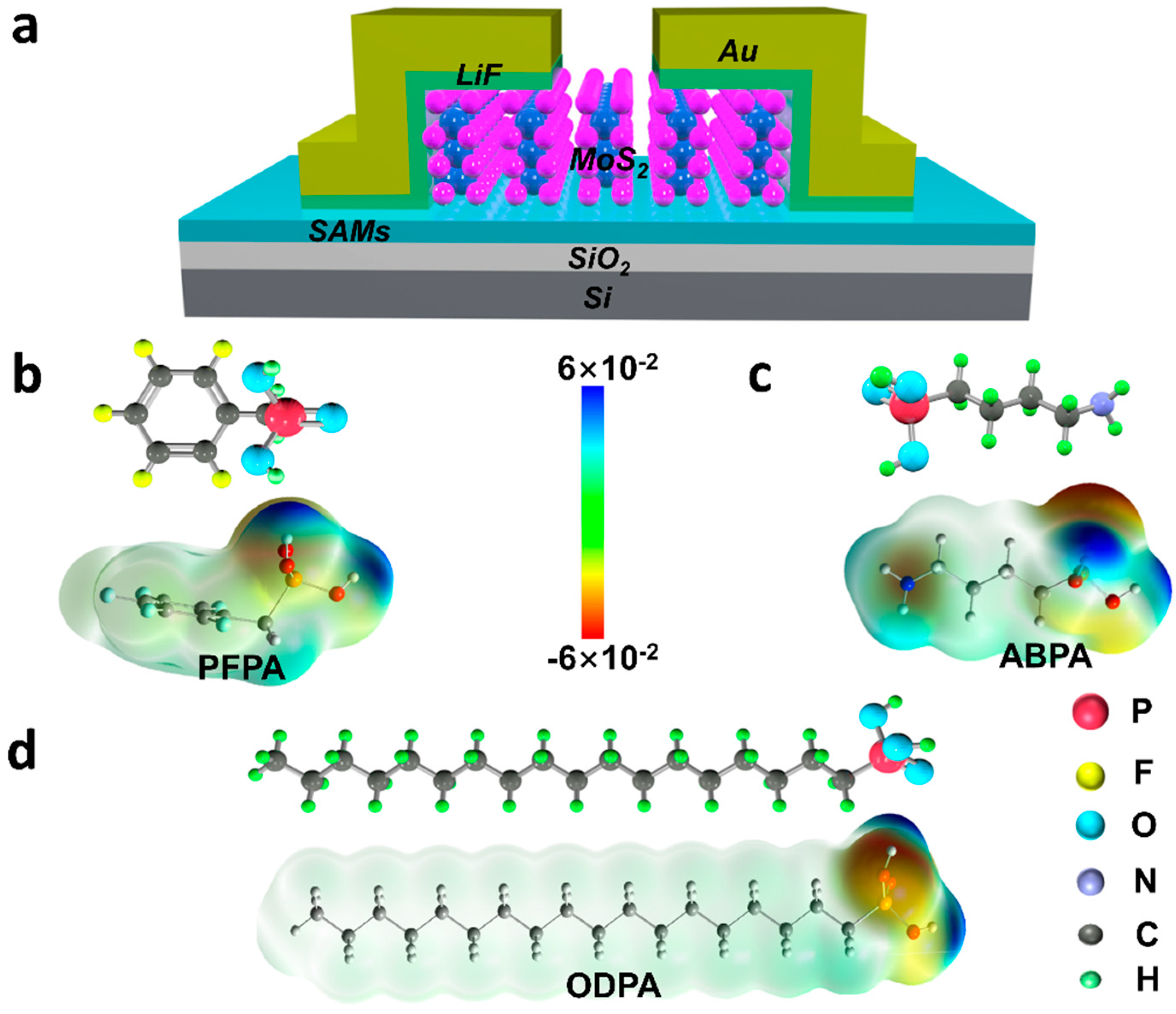
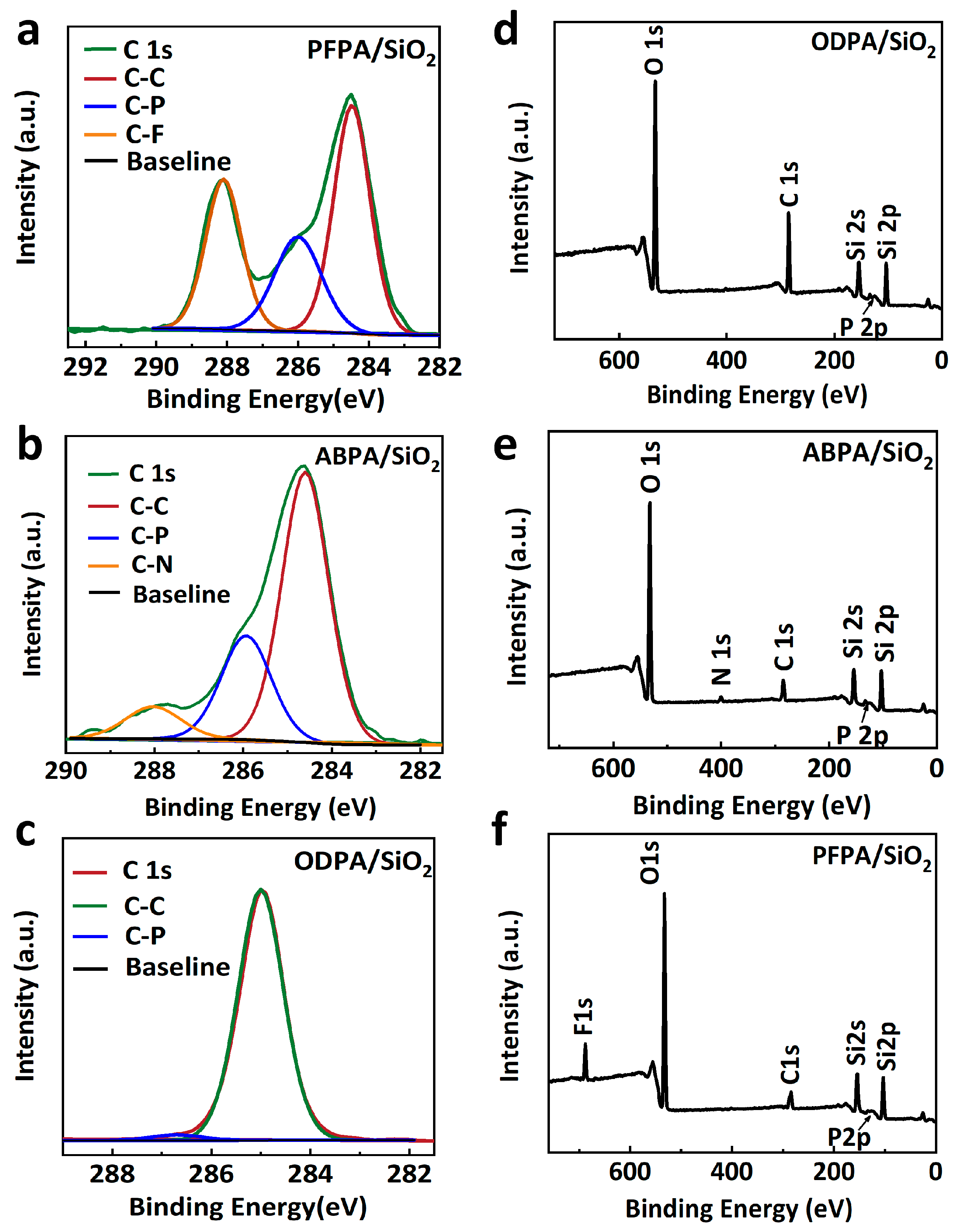
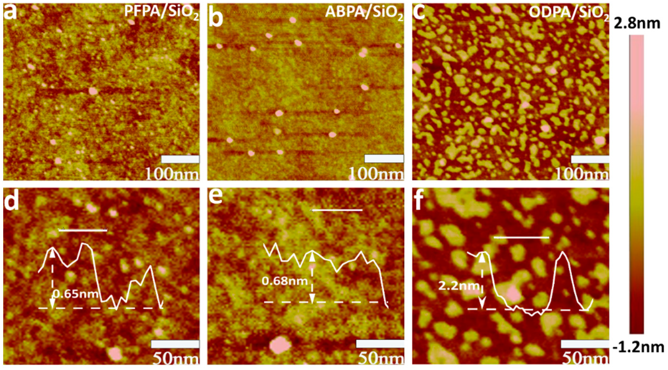
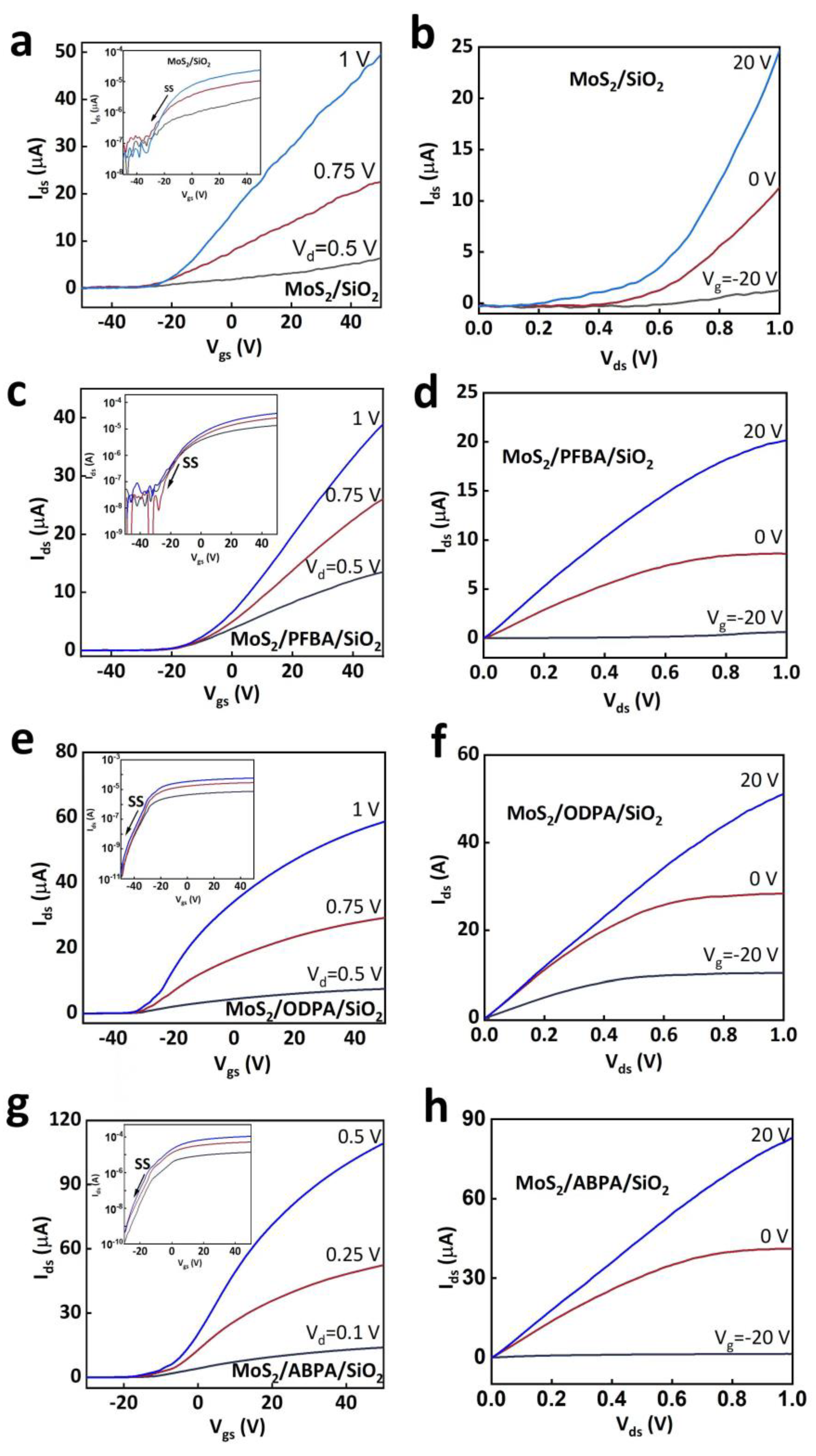
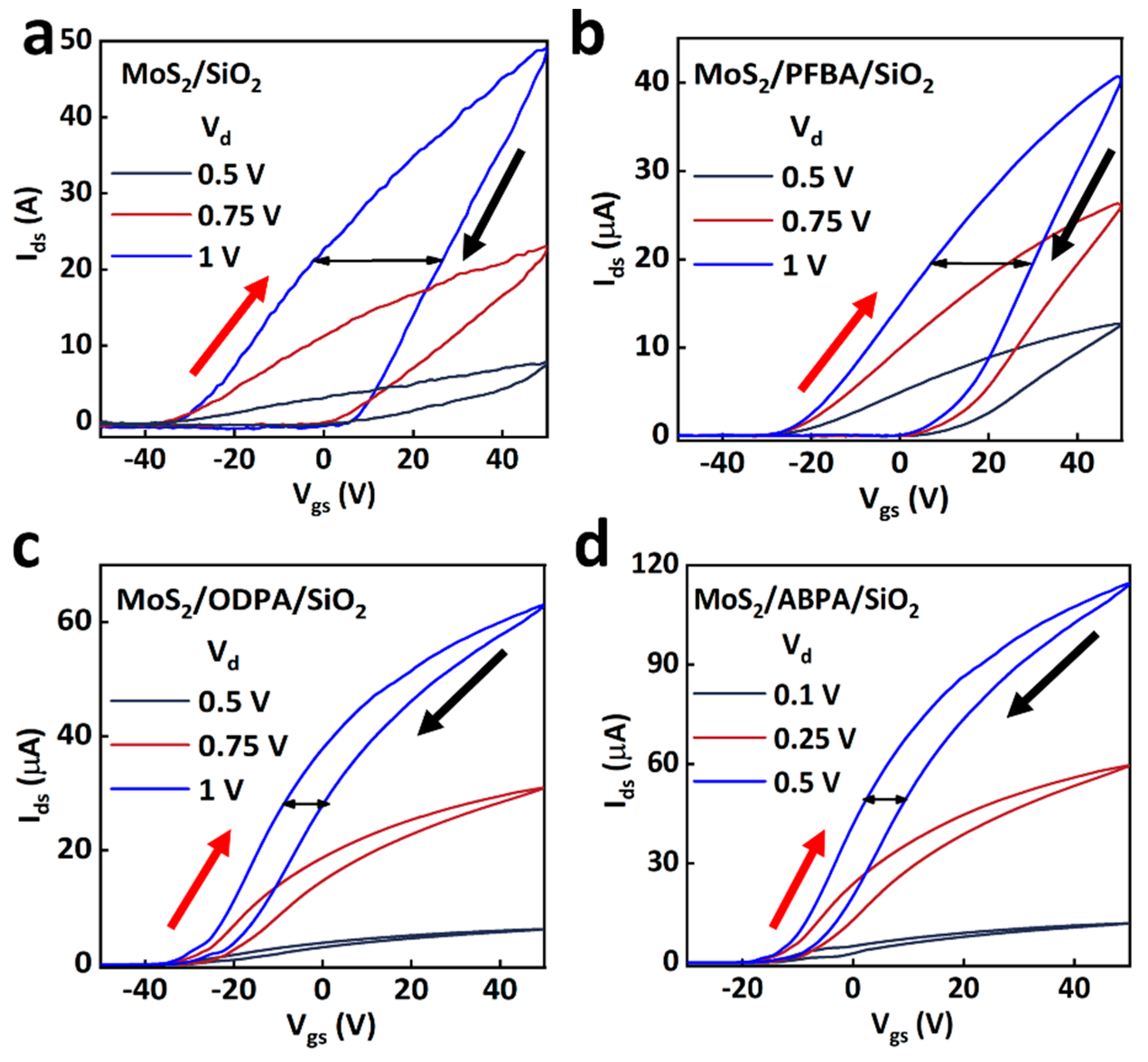
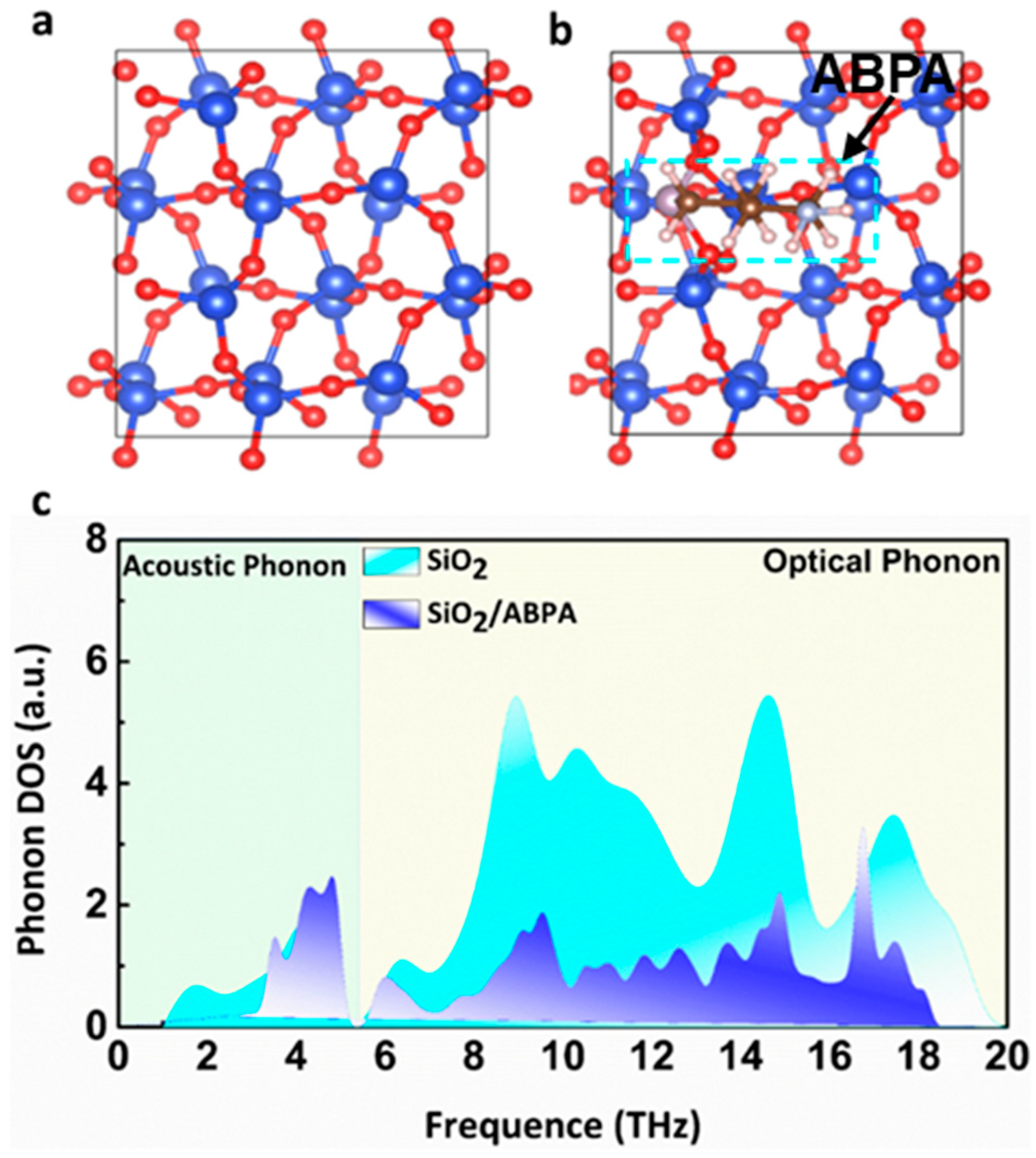
2. Results and Discussion
3. Conclusions
4. Experimental Section
Supplementary Materials
Author Contributions
Funding
Institutional Review Board Statement
Informed Consent Statement
Data Availability Statement
Conflicts of Interest
References
- Jones, A.M.; Yu, H.; Ghimire, N.J.; Wu, S.; Aivazian, G.; Ross, J.S.; Zhao, B.; Yan, J.; Man-drus, D.G.; Xiao, D.; et al. Optical generation of excitonic valley coherence in monolayer WSe2. Nat. Nanotechnol. 2013, 8, 634–638. [Google Scholar] [CrossRef]
- Pak, S.; Lee, J.; Lee, Y.; Jang, A.; Ahn, S.; Ma, K.Y.; Cho, Y.; Hong, J.; Lee, S.; Jeong, H.Y.; et al. Strain-mediated interlayer coupling effects on the excitonic behaviors in an epitaxially grown MoS2/WS2 van der waals heterobilayer. Nano Lett. 2017, 17, 5634–5640. [Google Scholar] [CrossRef] [PubMed]
- Chhowalla, M.; Jena, D.; Zhang, H. Two-dimensional semiconductors for transistors. Nat. Rev. Mater. 2016, 1, 16052. [Google Scholar] [CrossRef]
- Radisavljevic, B.; Whitwick, M.B.; Kis, A. Integrated circuits and logic operations based on single-layer MoS2. ACS Nano 2011, 5, 9934–9938. [Google Scholar] [CrossRef] [PubMed]
- Das, S.; Appenzeller, J. Where does the current flow in two-dimensional layered systems? Nano Lett. 2013, 13, 3396–3402. [Google Scholar] [CrossRef] [PubMed]
- Kaasbjerg, K.; Thygesen, K.S.; Jacobsen, K.W. Phonon-limited mobility in n-type single-layer MoS2 from first principles. Phys. Rev. B 2012, 85, 115317. [Google Scholar] [CrossRef]
- Ma, N.; Jena, D. Charge scattering and mobility in atomically thin semiconductors. Phys. Rev. X 2014, 4, 011043. [Google Scholar] [CrossRef]
- Illarionov, Y.Y.; Knobloch, T.; Jech, M.; Lanza, M.; Akinwande, D.; Vexler, M.I.; Mueller, T.; Lemme, M.C.; Fiori, G.; Schwierz, F.; et al. Insulators for 2D nanoelectronics: The gap to bridge. Nat. Commun. 2020, 11, 3385. [Google Scholar] [CrossRef]
- Kim, H.G.; Lee, H. Atomic layer deposition on 2D materials. Chem. Mater. 2017, 29, 3809–3826. [Google Scholar] [CrossRef]
- Li, W.; Zhou, J.; Cai, S.; Yu, Z.; Zhang, J.; Fang, N.; Li, T.; Wu, Y.; Chen, T.; Xie, X.; et al. Uniform and ultrathin high-kappa gate dielectrics for two-dimensional electronic devices. Nat. Electron. 2019, 2, 563–571. [Google Scholar] [CrossRef]
- Ng, H.K.; Xiang, D.; Suwardi, A.; Hu, G.; Yang, K.; Zhao, Y.; Liu, T.; Cao, Z.; Liu, H.; Li, S.; et al. Improving carrier mobility in two-dimensional semiconductors with rippled materials. Nat. Electron. 2022, 5, 489–496. [Google Scholar] [CrossRef]
- Liu, Y.; Guo, J.; Zhu, E.; Liao, L.; Lee, S.; Ding, M.; Shakir, I.; Gambin, V.; Huang, Y.; Duan, X. Approaching the Schottky–Mott limit in van der Waals metal–semiconductor junctions. Nature 2018, 557, 696–700. [Google Scholar] [CrossRef] [PubMed]
- Baugher, B.W.H.; Churchill, H.O.H.; Yang, Y.; Jarillo-Herrero, P. Intrinsic electronic transport properties of high-quality monolayer and bilayer MoS2. Nano Lett. 2013, 13, 4212–4216. [Google Scholar] [CrossRef] [PubMed]
- Yu, Z.; Pan, Y.; Shen, Y.; Wang, Z.; Ong, Z.; Xu, T.; Xin, R.; Pan, L.; Wang, B.; Sun, L.; et al. Towards intrinsic charge transport in monolayer molybdenum disulfide by defect and interface engineering. Nat. Commun. 2014, 5, 5290. [Google Scholar] [CrossRef]
- Paniagua, S.A.; Giordano, A.J.; Smith, O.L.; Barlow, S.; Li, H.; Armstrong, N.R.; Pemberton, J.E.; Bredas, J.; Ginger, D.; Marder, S.R. Phosphonic acids for interfacial engineering of transparent conductive oxides. Chem. Rev. 2016, 116, 7117–7158. [Google Scholar] [CrossRef]
- Timpel, M.; Li, H.; Nardi, M.V.; Wegner, B.; Frisch, J.; Hotchkiss, P.J.; Marder, S.R.; Barlow, S.; Bredas, J.; Koch, N. Electrode work function engineering with phosphonic acid monolayers and molecular acceptors: Charge redistribution mechanisms. Adv. Funct. Mater. 2018, 28, 1704438. [Google Scholar] [CrossRef]
- Benneckendorf, F.S.; Hillebrandt, S.; Ullrich, F.; Rohnacher, V.; Hietzschold, S.; Jaensch, D.; Freudenberg, J.; Beck, S.; Mankel, E.; Jaegermann, W.; et al. Structure-property relationship of phenylene-based self-assembled monolayers for record low work function of indium tin oxide. J. Phys. Chem. Lett. 2018, 9, 3731–3737. [Google Scholar] [CrossRef]
- Wang, B.; Di Carlo, G.; Turrisi, R.; Zeng, L.; Stallings, K.; Huang, W.; Bedzyk, M.J.; Beverina, L.; Marks, T.J.; Facchetti, A. The dipole moment inversion effects in self-assembled nanodielectrics for organic transistors. Chem. Mater. 2017, 29, 9974–9980. [Google Scholar] [CrossRef]
- Hotchkiss, P.J.; Jones, S.C.; Paniagua, S.A.; Sharma, A.; Kippelen, B.; Armstrong, N.R.; Marder, S.R. The modification of indium tin oxide with phosphonic acids: Mechanism of Binding, Tuning of Surface Properties, and Potential for Use in Organic Electronic Applications. Acc. Chem. Res. 2012, 45, 337–346. [Google Scholar] [CrossRef] [PubMed]
- Kuo, L.; Sangwan, V.K.; Rangnekar, S.V.; Chu, T.C.; Lam, D.; Zhu, Z.; Richter, L.J.; Li, R.; Szydłowska, B.M.; Downing, J.R.; et al. All-printed ultrahigh-responsivity MoS2 nanosheet photodetectors enabled by megasonic exfoliation. Adv. Mater. 2022, 34, 2203772. [Google Scholar] [CrossRef]
- Yokota, K.; Takai, K.; Enoki, T. Carrier control of graphene driven by the proximity effect of functionalized self-assembled monolayers. Nano Lett. 2011, 11, 3669–3675. [Google Scholar] [CrossRef]
- Kobayashi, S.; Nishikawa, T.; Takenobu, T.; Mori, S.; Shimoda, T.; Mitani, T.; Shimotani, H.; Yoshimoto, N.; Ogawa, S.; Iwasa, Y. Control of carrier density by self-assembled monolayers in organic field-effect transistors. Nat. Mater. 2004, 3, 317–322. [Google Scholar] [CrossRef]
- Nasr, J.R.; Simonson, N.; Oberoi, A.; Horn, M.W.; Robinson, J.A.; Das, S. Low-power and ultra-thin MoS2 photodetectors on glass. ACS Nano 2020, 14, 15440–15449. [Google Scholar] [CrossRef]
- Lu, D.; Chen, Y.; Kong, L.; Luo, C.; Lu, Z.; Tao, Q.; Song, W.; Ma, L.; Li, Z.; Li, W.; et al. Strain-plasmonic coupled broadband photodetector based on monolayer MoS2. Small 2022, 18, 2107104. [Google Scholar] [CrossRef]
- Cho, H.; Kang, D.; Lee, Y.; Bae, H.; Hong, S.; Cho, Y.; Kim, K.; Yi, Y.; Park, J.H.; Im, S. Dramatic reduction of contact resistance via ultrathin LiF in two-Dimensional MoS2 field effect transistors. Nano Lett. 2021, 21, 3503–3510. [Google Scholar] [CrossRef]
- Bardecker, J.A.; Ma, H.; Kim, T.; Huang, F.; Liu, M.S.; Cheng, Y.; Ting, G.; Jen, A.K.Y. Self-assembled electroactive phosphonic acids on ITO: Maximizing hole-injection in polymer light-emitting diodes. Adv. Funct. Mater. 2008, 18, 3964–3971. [Google Scholar] [CrossRef]
- Cheng, H.; Huai, J.; Cao, L.; Li, Z. Novel self-assembled phosphonic acids monolayers applied in N-channel perylene diimide (PDI) organic field effect transistors. Appl. Surf. Sci. 2016, 378, 545–551. [Google Scholar] [CrossRef]
- Rozlosnik, N.; Gerstenberg, M.C.; Larsen, N.B. Effect of solvents and concentration on the formation of a self-assembled monolayer of octadecylsiloxane on silicon (001). Langmuir 2003, 19, 1182–1188. [Google Scholar] [CrossRef]
- Choi, Y.; Kim, H.; Yang, J.; Shin, S.W. Proton-Conductor-Gated MoS2 Transistors with Room Temperature Electron Mobility of >100 cm2 V−1 s−1. Chem. Mater. 2018, 30, 4527–4535. [Google Scholar] [CrossRef]
- Liu, N.; Baek, J.; Kim, S.M.; Hong, S.; Hong, Y.K.; Kim, Y.S.; Kim, H.; Kim, S.; Park, J. Improving the stability of high-performance multilayer MoS2 field-effect transistors. ACS Appl. Mater. Interfaces 2017, 9, 42943–42950. [Google Scholar] [CrossRef]
- Guo, Y.; Wei, X.; Shu, J.; Liu, B.; Yin, J.; Guan, C.; Han, Y.; Gao, S.; Chen, Q. Charge trapping at the MoS2-SiO2 interface and its effects on the characteristics of MoS2 metal-oxide-semiconductor field effect transistors. Appl. Phys. Lett. 2015, 106, 103109. [Google Scholar] [CrossRef]
- Cui, X.; Lee, G.; Kim, Y.D.; Arefe, G.; Huang, P.Y.; Lee, C.; Chenet, D.A.; Zhang, X.; Wang, L.; Ye, F.; et al. Multi-terminal transport measurements of MoS2 using a van der Waals heterostructure device platform. Nat. Nanotechnol. 2015, 10, 534–540. [Google Scholar] [CrossRef]
- Aghamohammadi, M.; Rödel, R.; Zschieschang, U.; Ocal, C.; Boschker, H.; Weitz, R.T.; Barrena, E.; Klauk, H. Threshold-voltage shifts in organic transistors due to self-assembled monolayers at the dielectric: Evidence for electronic coupling and dipolar effects. ACS Appl. Mater. Interfaces 2015, 7, 22775–22785. [Google Scholar] [CrossRef]
- Chung, Y.; Verploegen, E.; Vailionis, A.; Sun, Y.; Nishi, Y.; Murmann, B.; Bao, Z. Controlling electric dipoles in nanodielectrics and its applications for enabling air-stable n-channel organic transistors. Nano Lett. 2011, 11, 1161–1165. [Google Scholar] [CrossRef]
- Cheng, L.; Zhang, C.; Liu, Y. Why Two-dimensional semiconductors generally have low electron mobility. Phys. Rev. Lett. 2020, 125, 177701. [Google Scholar] [CrossRef]
- Kresse, G.; Furthmuller, J. Efficient iIterative schemes for ab initio total-energy calculations using a plane-wave basis set. Phys. Rev. B 1996, 54, 11169–11186. [Google Scholar] [CrossRef]
- Perdew, J.P.; Burke, K.; Ernzerhof, M. Generalized gradient approximation made simple. Phys. Rev. Lett. 1996, 77, 3865–3868. [Google Scholar] [CrossRef]
- Kresse, G.; Joubert, D. From ultrasoft pseudopotentials to the projector augmented-wave method. Phys. Rev. B 1999, 59, 1758–1775. [Google Scholar] [CrossRef]
- Blochl, P.E. Projector augmented-wave method. Phys. Rev. B 1994, 50, 17953–17979. [Google Scholar] [CrossRef]
- Grimme, S.; Antony, J.; Ehrlich, S.; Krieg, H.J. A consistent and accurate ab initio parametrization of density functional dispersion correction (DFT-D) for the 94 elements H-Pu. Chem. Phys. 2010, 132, 154104. [Google Scholar]
- Henkelman, G.; Uberuaga, B.P.; Jonsson, H.J. A climbing image nudged elastic band method for finding saddle points and minimum energy paths. Chem. Phys. 2000, 113, 9901. [Google Scholar] [CrossRef]
- Togo, A.; Tanaka, I. First principles phonon calculations in materials science. Scr. Mater. 2015, 108, 1–5. [Google Scholar] [CrossRef]


| SAMs | P (debye) | PZ (debye) | VSAMs (mV) |
|---|---|---|---|
| PFPA | −0.98 | 0.72 | −496 to −589 |
| ABPA | 2.15 | 2.04 | +1405 to +1668 |
| ODPA | 1.44 | 1.06 | +730 to+868 |
Disclaimer/Publisher’s Note: The statements, opinions and data contained in all publications are solely those of the individual author(s) and contributor(s) and not of MDPI and/or the editor(s). MDPI and/or the editor(s) disclaim responsibility for any injury to people or property resulting from any ideas, methods, instructions or products referred to in the content. |
© 2024 by the authors. Licensee MDPI, Basel, Switzerland. This article is an open access article distributed under the terms and conditions of the Creative Commons Attribution (CC BY) license (https://creativecommons.org/licenses/by/4.0/).
Share and Cite
Cao, L.; Wei, J.; Li, X.; Wang, S.; Qin, G. Enhancing the Performance of MoS2 Field-Effect Transistors Using Self-Assembled Monolayers: A Promising Strategy to Alleviate Dielectric Layer Scattering and Improve Device Performance. Molecules 2024, 29, 3988. https://doi.org/10.3390/molecules29173988
Cao L, Wei J, Li X, Wang S, Qin G. Enhancing the Performance of MoS2 Field-Effect Transistors Using Self-Assembled Monolayers: A Promising Strategy to Alleviate Dielectric Layer Scattering and Improve Device Performance. Molecules. 2024; 29(17):3988. https://doi.org/10.3390/molecules29173988
Chicago/Turabian StyleCao, Li, Junqing Wei, Xianggao Li, Shirong Wang, and Guoxuan Qin. 2024. "Enhancing the Performance of MoS2 Field-Effect Transistors Using Self-Assembled Monolayers: A Promising Strategy to Alleviate Dielectric Layer Scattering and Improve Device Performance" Molecules 29, no. 17: 3988. https://doi.org/10.3390/molecules29173988
APA StyleCao, L., Wei, J., Li, X., Wang, S., & Qin, G. (2024). Enhancing the Performance of MoS2 Field-Effect Transistors Using Self-Assembled Monolayers: A Promising Strategy to Alleviate Dielectric Layer Scattering and Improve Device Performance. Molecules, 29(17), 3988. https://doi.org/10.3390/molecules29173988