Abstract
In this work, we investigated the influence of MoS2 functioning as an electron transport layer (ETL) on the inverted flexible organic photovoltaics (FOPVs). Three ETLs, including MoS2, lithium quinolate (Liq), and a MoS2/Liq bilayer, were evaporated onto ITO-integrated polyethylene terephthalate substrates (PET-ITO), and the properties of transmittance, water contact angle, and reflectivity of the films were analyzed. The results revealed that MoS2 was helpful to improve the lipophilicity of the surface of the ETL, which was conducive to the deposition of the active layer. In addition, the reflectivity of MoS2 to the light ranging from 400 to 600 nm was the largest among the pristine PET-ITO substrate and the PET-ITO coated with three ETLs, which promoted the efficient use of the light. The efficiency of the FOPV with MoS2/Liq ETL was 73% higher than that of the pristine device. This was attributed to the nearly two-fold amplification of the MoS2 array to the light field, which promoted the FOPV to absorb more light. Moreover, the efficiency of the FOPV with MoS2 was maintained under different illumination angles and bending angles. The results demonstrate the promising applications of MoS2 in the fabrication of FOPVs.
1. Introduction
Flexible organic photovoltaics (FOPVs) have become one of the hottest directions in the field of OPV research [1,2]. Neither the traditional silicon solar cells nor the emerging perovskite solar cells can be comparable with FOPV in applications requiring flexible properties. Polyethylene terephthalate (PET), which has the characteristics of light weight and bending resistance, is a widely used ideal flexible substrate in organic electronic devices, including organic field-effect transistors [3,4,5], organic light emitting diodes [6,7], and FOPVs [8,9]. The research on FOPV primarily focuses on developing new polymeric functional materials [10,11], electrodes [12,13,14,15,16,17,18], and substrates [19,20,21,22]. In addition, fabrication technology is also one of the most widely researched areas to obtain an FOPV [23,24,25,26]. Nowadays, introducing an intermediate layer between the electrode and the functional layer as an electron transport layer (ETL) to improve the performance of the FOPVs has attracted intensive attention [27,28,29,30,31].
Two-dimensional (2D) materials are a class of widely researched ETLs due to their merits of high optical transparency, high charge carrier mobility, high stability, and tunable work function [32,33,34,35]. The tunable energy gap and excellent magnetic behaviors of MoS2 make it one of the most attractive 2D materials in applications in ETLs [32,36,37,38,39]. Lee et al. reported an inverted OPV integrating MoS2 nanosheet as the ETL [40]. They revealed that the MoS2 nanosheet played an important role as a sub-photo sensitizer and an ETL, providing effective charge separation in the OPV. However, a deeper analysis of the performance improvement of FOPVs brought by MoS2 is still needed.
This work investigated the application of a MoS2 micro-nano array as an ETL in FOPV. Three ETLs, which are lithium quinolate (Liq), MoS2, and a MoS2/Liq bilayer, were applied in FOPV. Then the performance differences between the ETLs were studied by analyzing their transmittance, water contact angle, and reflectivity. The results revealed that MoS2 was helpful to improve lipophilicity, which was conducive to the deposition of the active layer. The reflectivity of MoS2 to the light ranging from 400 to 600 nm was the largest, which promoted the efficient use of the light. The efficiency of the FOPV with MoS2 EIL was 73% higher than that of the pristine FOPV. This was primarily attributed to the nearly two-fold amplification of the MoS2 array to the light field, which promoted the FOPV to absorb more light. Moreover, the efficiency of the FOPV with MoS2 was maintained under different illumination angles and bending angles. The results demonstrate the promising applications of MoS2 in the fabrication of FOPVs.
2. Results and Discussion
2.1. Characterization of the ETLs
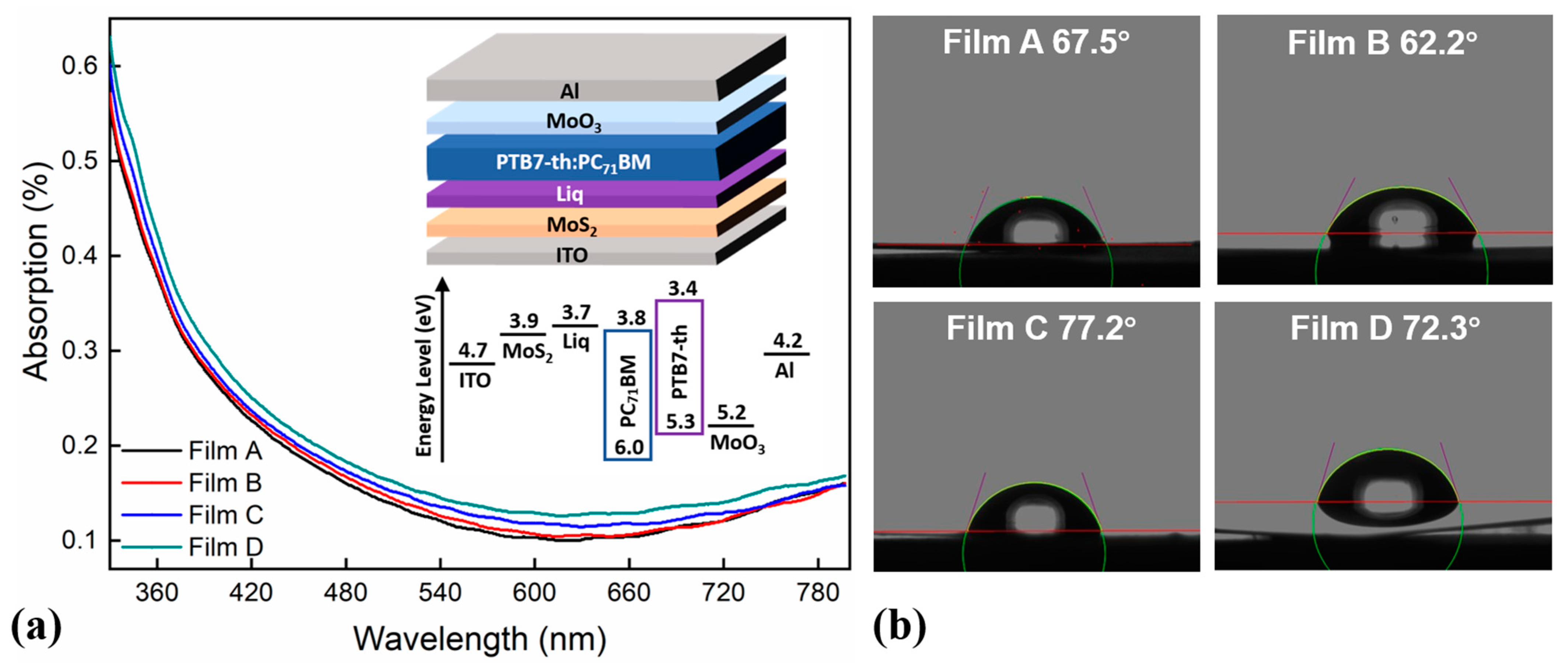
The characteristics of the four kinds of films were explored in detail on the basis of transmittance, absorption, water contact angle, and reflectivity. The films containing different ETLs on the PET-ITO substrate were defined as Film A (without ETL), Film B (with Liq ETL), Film C (with MoS2 ETL), and Film D (with MoS2/Liq ETL), respectively.
Figure 1a shows the results of the absorbance properties of the four films. It can be found that if we sort the absorbance in ascending order, then the order of the films is Film A, Film B, Film C, and Film D. The transmittance calculated using the Beer–Lambert Law followed the opposite trend. Meanwhile, although the results were different from each other, there was little difference in general. It could be concluded from the results that the absorbance of the films had a slight relationship with the morphology and the structure of the film but showed a direct relationship with the thickness of the film.

Figure 1.
(a) Absorbance properties of Films A, B, C, and D; inset is the structure and energy level of Device D. (b) The water contact angles of Films A, B, C, and D.
Figure 1b describes the water contact angles of the four films, where it can be found that the water contact angles of Film A, Film B, Film C, and Film D are 67.5°, 62.2°, 77.2°, and 72.3°, respectively. These results indicated that Liq was helpful to improve the hydrophilicity of the film surface, while MoS2 was helpful to improve the lipophilicity of the film. The increased lipophilicity could decrease the surface energy difference between the ETL and the active layer [41]. Since the interfacial energy affects the thermodynamic miscibility between two adjacent layers, it is thus indicated that MoS2 possesses excellent miscibility with the active layer, conducive to the deposition of the active layer grown on top of the ETL.
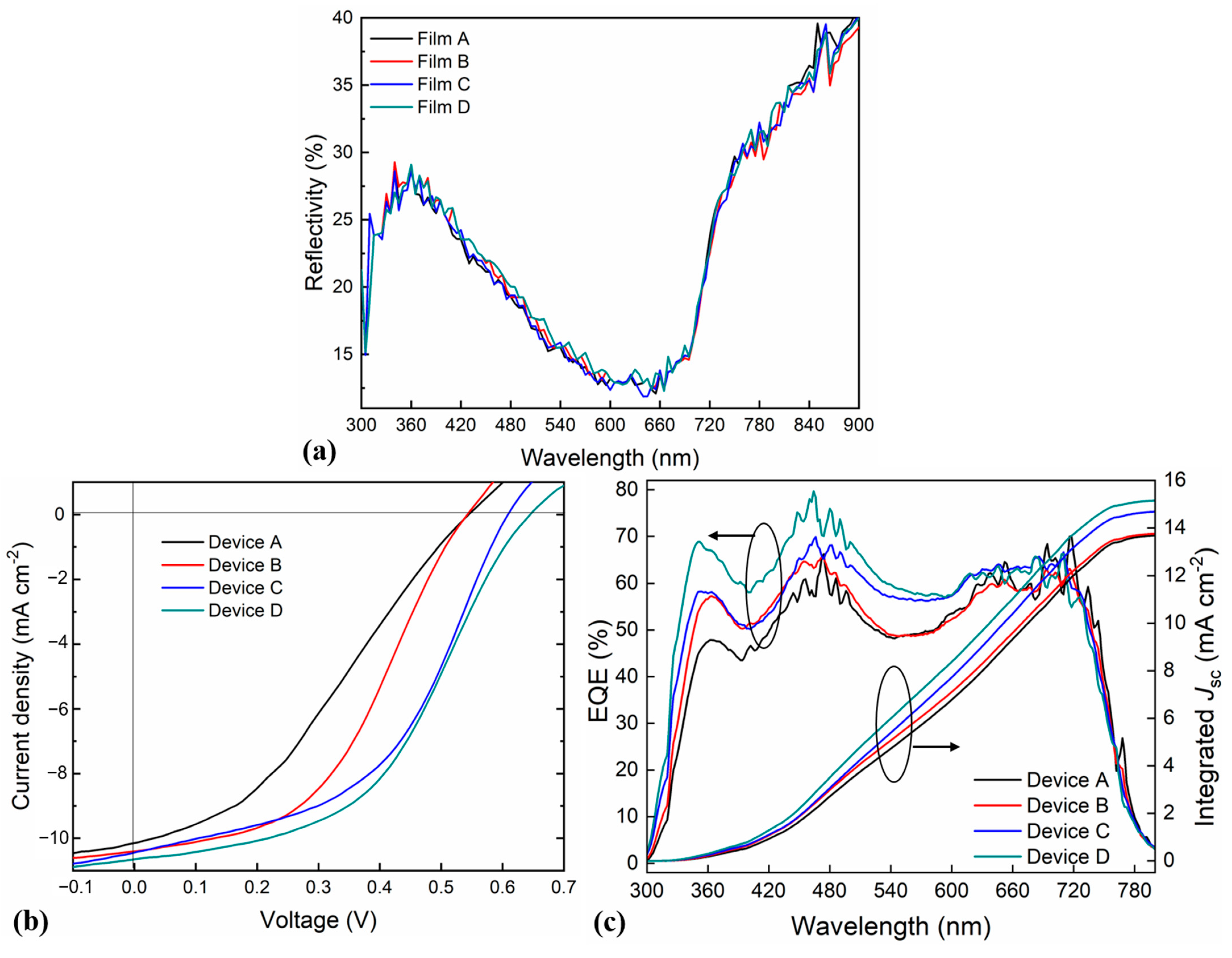
Figure 2a shows the reflectivity test of the four films. It can be seen from the results that the reflectivity of the four films is almost unchanged. One exception is that if the incident wavelength of the light ranges from 400 to 600 nm, the reflectivity of Film C is the largest among the four films. Here, we suppose the large reflectivity of Film C was primarily due to its nano-array morphology. The light was reflected and scattered in the arrayed structure, which led to high reflectivity. Meanwhile, the relatively thick thickness of MoS2 (10 nm) compared to that of Liq (3 nm) could also be the cause for its high reflectivity. In addition, there might be a waveguide function of the nano-array structure, which could further limit the transmission of light [42]. To make the active layer absorb more light, it was better if more light could be reflected by both sides of the films. Therefore, MoS2 was preferred as the ETL to promote the effective use of the light.
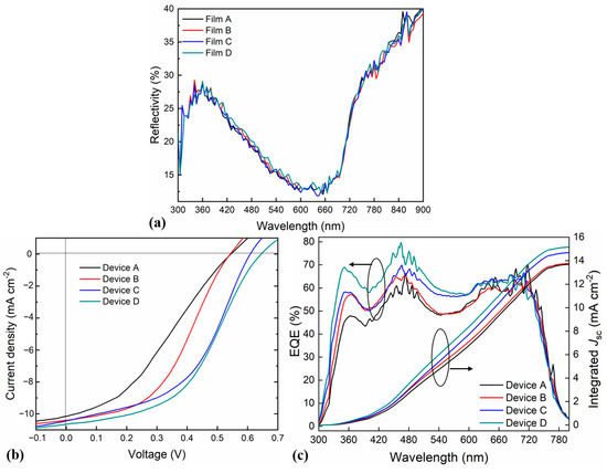
Figure 2.
(a) The reflectivity test of Films A, B, C, and D. (b) The JV characteristic curves and (c) EQE and integrated Jsc analyses of Devices A, B, C, and D.
2.2. Effect of Difference ETLs on the Performance of FOPVs
The J-V test for four devices is shown in Figure 2b. It can be seen from Figure 2b that Device D outperforms the other three devices in terms of PCE, open-circuit voltage (Voc), and short-circuit current density (Jsc). Despite that the Voc and the Jsc of Device C are not as good as those of Device D, its filling factor (FF) is the highest among the four films. The Voc and the Jsc of Devices A and B are nearly the same, but Device B has a larger FF than Device A. Since the work function of MoS2 is located between that of ITO and the LUMO of PC71BM, as shown in the inset of Figure 1a, the Voc of Devices C and D was optimized. The corresponding values of the four devices (averaged from three devices) are summarized in Table 1. The performance of Device B is optimized compared to that of Device A, which is further increased in Device D. The Voc, Jsc, FF, and PCE of Device D are 0.66 V, 10.66 mA cm−2, 46.71%, and 3.3%, respectively, which are the best among the four devices. The PCE of Device C and Device D increased by 63% and 73% compared to that of Device A. In addition, the J-V characteristic curves of the four devices are all “S-shaped”, which means that there exists a leakage current between layers, and hence, there still exists an opportunity for the optimization of the device structure. Meanwhile, the external quantum efficiency (EQE) and integrated Jsc were also analyzed. As shown in Figure 2c, the performance of Device D possessed was the best, with an EQE of over 70% at 450–500 nm and an integrated Jsc of 15.15 mA/cm2.

Table 1.
The values of the four inherent parameters of the four devices.
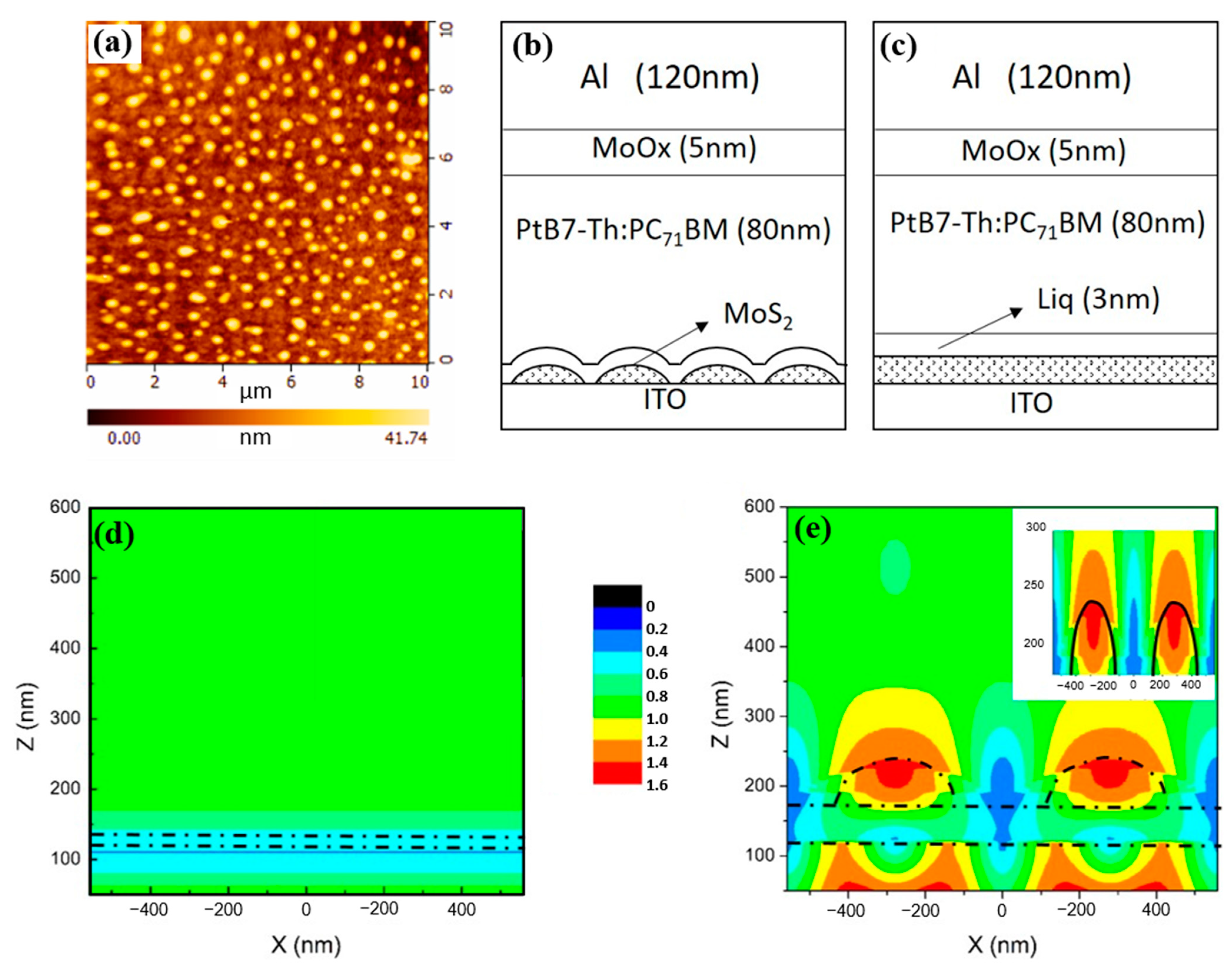
From the above analyses, it could be concluded that the performance of FOPV containing MoS2/Liq ETL was significantly better than others. To illustrate the conclusion in detail, we analyzed the surface morphology of the MoS2 ETL. As depicted in Figure 3a, the MoS2 is no longer a thin film in terms of morphology, but rather a micro-nano array with the ability of light field amplification. The schematic diagram of the devices with the MoS2 array and Liq film is presented in Figure 3b,c. The micro-nano array MoS2 showed the optical field amplification effect, leading to the absorption of more light. To reveal the influence of the MoS2 array on the performance of the FOPV, we further adapted the FDTD simulation to investigate the light field of the films. As can be seen from Figure 3d,e, the amplification effect of the MoS2 array on the light field is significantly demonstrated. The intensity of the light field in the active layer is nearly doubled compared to the device without an array structure. This ability promoted the FOPV to absorb more light, which contributes to enhanced device performance.

Figure 3.
(a) AFM image of MoS2 array. Schematic diagram of the devices with (b) MoS2 array structure and (c) without array structure. Optical simulation of (d) MoS2 grown on PET substrate (without the nano-array structure) and (e) MoS2 grown on PET-ITO substrate (with the nano-array structure); the insets show the light intensity distribution of the film at the thickness of 175–300 nm.
2.3. Performance of FOPV with Different Illumination and Bending Angles
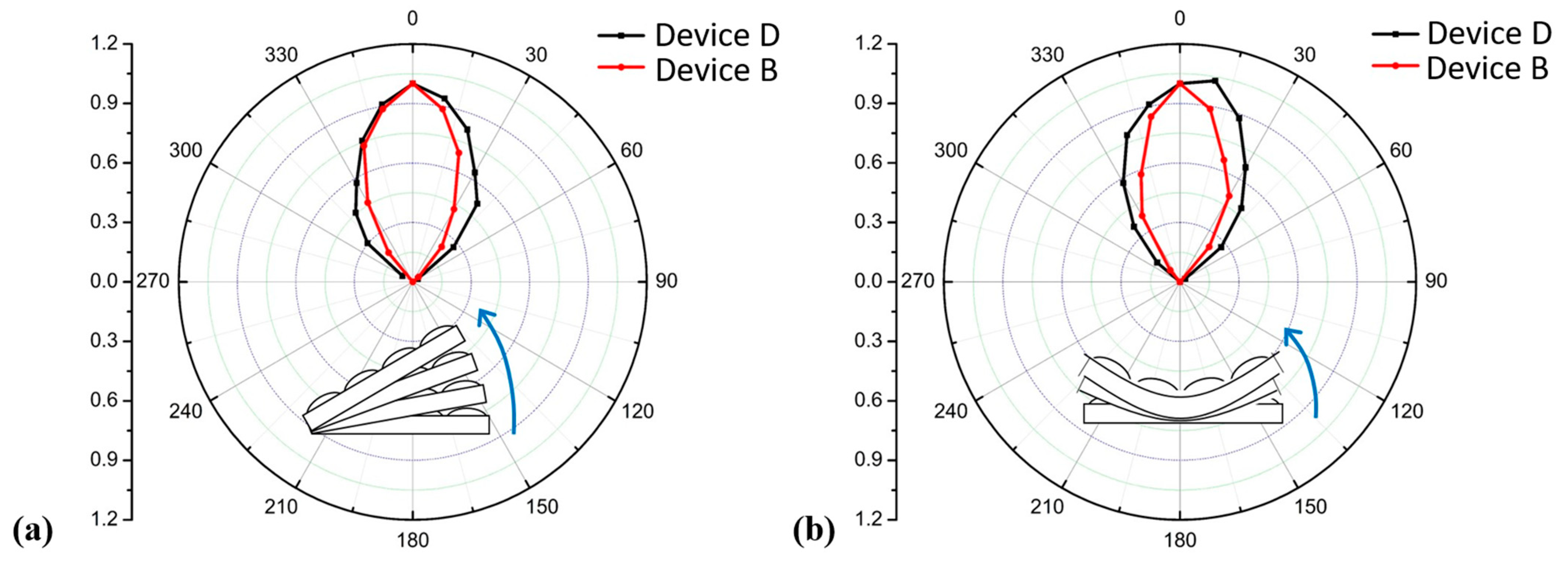
The relationship between the efficiencies of the devices and illumination angles is shown in Figure 4a. The black line represents Device D, while the red line is Device B. The data were obtained by dividing the actual efficiency by the initial efficiency. It can be seen from Figure 4a that the efficiency of Device D decays slowly with the change in the illumination angle, which is of great significance in practical applications. The light angle sensitivity of organic photovoltaic devices seriously affects the total energy collected by the devices, while the use of a MoS2 array can greatly reduce the light angle sensitivity of the device, which allows the device to collect light energy more effectively at different time periods in practical applications. Therefore, the energy loss caused by the light angle was reduced, and the application of the FOPV was greatly broadened.
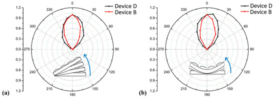
Figure 4.
Device efficiency of Devices B and D under different (a) illumination angles and (b) bending angles.
For FOPV, not only the illumination angle but also the bending angle plays an indispensable role in the practical application of the device, especially when the devices are applied to the surface of flexible objects such as curtains, backpacks, and solar sails, which cannot maintain a fixed angle for collecting the light source. Therefore, it is important to maintain the performance under different bending angles of the objects to which the devices are applied. Figure 4b shows the efficiency changes of the device under different bending angles. It can be seen from Figure 4b that not only is the device containing MoS2 insensitive to the bending angle, but its efficiency is also higher than the initial efficiency, even though the bending angle is approximately 10°. Hence, the device containing MoS2 was very conducive to its subsequent practical application.
3. Experimental Section
3.1. Materials and Device Fabrication
The PET-ITO substrates (30 per sheet, 150 nm) were purchased from Shanghai Quanhua Trading Co. Ltd., and the average transmittance of the substrate at 400 to 700 nm was 70%. MoS2 powder (98%, 5.06 g/mL at room temperature, particle size < 2 μm) and aluminum (99%) were purchased from Sigma Aldrich. Liq (99%, light yellow powder), MoO3 (99%, white powder), donor material PTB7-Th, and acceptor material PC71BM (99%, black organic material) were all purchased from Lumtec Optoelectronic Materials Co. Ltd. The proportioning method for the construction of the active layer is given here. The weight ratio of the PTB7-Th:PC71BM solvent was 2:3. The solvent was produced by mixing the chlorobenzene and the 1,8-diiodooctane according to the ratio of 97:3. The vacuum evaporation equipment used to thermally evaporate ETLs was purchased from Shenyang Lining Vacuum Co., Ltd. (Shenyang, China). MoS2 was placed on the tungsten boat and fixed between two electrodes in the evaporation chamber. Then, the chamber was vacuumed to 10−4 mbar, and the current source was turned on to evaporate the MoS2. Liq was put in a crucible surrounded by the heating source and was sublimated at 260−270 °C. A crystal oscillator located on the top of the chamber (controlled by the Deposition Controller, INFICON) was used to detect the rate of evaporation and the thickness of the film. We kept the lifetime of the oscillator above 85% to guarantee its high accuracy. For each ETL, we used atomic force microscope (AFM) analysis to measure their thicknesses, and the calibration parameter between the test and measured thickness was set in the Deposition Controller. Therefore, the error of the detected thickness of 10 nm (MoS2) and 3 nm (Liq) was less than 0.2 nm.
There are four kinds of FOPVs with different ETLs. The pristine structure was ITO (200 nm)/ETLs/PTB7-Th:PC71BM (80 nm)/MoO3 (5 nm)/Al (120 nm). We defined Device A as the pristine FOPV without an ETL, Device B with 3 nm Liq, Device C with 10 nm MoS2, and Device D with MoS2 (10 nm)/Liq (3 nm) as the ETL. The structure and energy level of Device D are shown in the inset of Figure 1a.
The PET-ITO substrates were ultrasonically cleaned in deionized water, acetone, and isopropanol sequentially and were dried under the tungsten lamp. Then, the substrates were UV-ozone treated for five minutes. The ETLs were thermally evaporated onto the substrate at a rate of 0.3 Å/s, and then PTB7-Th:PC71BM was spin-coated at a speed of 1000 rpm for 90 s. The spin-coated substrate was wiped with a cotton swab with chloroform to expose the electrodes. The substrate was moved into the evaporation chamber again and was vacuumized for 1 h to pump away the solvent. Then, 5 nm MoO3 was evaporated onto the active layer, and a 120 nm Al electrode was deposited.
3.2. Characterization
The FOPVs were connected to the external power supply and then continuously exposed to light with an intensity of 100 mWcm−2. The programmable light source meter (Keithley 2400) and the sunlight simulator AM 1.5 G were used to simulate the solar spectrum to collect the J-V characteristic curve of the device. All performance tests were carried out in the environment without encapsulated devices.
Water contact angle measurement was analyzed to reveal the wettability of the film surface by measuring the liquid–solid contact angle. In this test, the contact angle goniometer was used to measure the surface tension, wettability, and other information of deionized water and different substrates. The measurement method was a circle-fitting method.
The reflectivity test was based on the external quantum efficiency (EQE) detection platform. The 7-SCSpec solar cell measurement system manufactured by the 7-STAR company was used to first test the reflectance spectrum of the standard white plate and then test the reflectance spectrum of the sample. Eventually, the reflectivity of the sample was calculated by using the standard reflectivity.
The basic principle of the transmittance test can be described as follows: When the incident light is exposed to the surface of the sample, part of the light passing through the sample can be collected by the machine, and then the transmittance of the sample at each frequency can be obtained by comparing the wavelengths of the incident light and the collected light. The basic principle of the absorbance test is to record the absorption spectrum by taking advantage of the transition phenomenon produced when the molecules in the sample are absorbing ultraviolet and visible light. The relationship between the transmittance and the absorbance satisfies Formula (1) (Beer–Lambert Law):
where A is the absorbance, T is the transmittance, K is the molar absorption coefficient, b is the sample thickness, and c is the sample concentration.
4. Conclusions
In summary, we investigated the influence of MoS2 ETL on the inverted flexible FOPVs. The properties of the ETLs, including transmittance, the water contact angle, and reflectivity, were systematically analyzed. The results revealed that MoS2 was helpful to improve the lipophilicity of the surface of the ETL, which was conducive to the deposition of the active layer. The reflectivity of MoS2 to light ranging from 400 to 600 nm was the largest among the pristine PET-ITO substrate and the PET-ITO coated with three ETLs, which promoted the efficient use of the light. The efficiency of the FOPV with MoS2 EIL was 73% higher than that of the pristine device. This was primarily attributed to the nearly two-fold amplification of the MoS2 array to the light field, which promoted the FOPV to absorb more light. Moreover, the efficiency of the FOPV with MoS2 was maintained under different illumination angles and bending angles. The results shed light on the promising applications of MoS2 in the fabrication of FOPVs.
Author Contributions
Conceptualization, B.W. and C.P.; methodology, Z.L.; software, Z.L. and C.P; validation, C.C.; formal analysis, M.Q.; investigation, G.C.; resources, Z.L.; data curation, Z.L.; writing—original draft preparation, C.P., W.S. and Z.L.; writing—review and editing, W.S.; supervision, W.S. and B.W.; funding acquisition, B.W. All authors have read and agreed to the published version of the manuscript.
Funding
This work was financially supported by the State’s Key Project of Research and Development Plan (2022YFE0109000) and the National Natural Science Foundation of China (11974236).
Institutional Review Board Statement
Not applicable.
Informed Consent Statement
Not applicable.
Data Availability Statement
Data is available from authors upon reasonable requirement.
Conflicts of Interest
The authors declare no conflict of interest.
Sample Availability
Samples of the compounds. are available from the authors upon reasonable requirement.
References
- Xu, G.; Hu, X.; Liao, X.; Chen, Y. Bending-stability Interfacial Layer as Dual Electron Transport Layer for Flexible Organic Photovoltaics. Chin. J. Polym. Sci. 2021, 39, 1441–1447. [Google Scholar] [CrossRef]
- Park, Y.; Berger, J.; Tang, Z.; Mueller-Meskamp, L.; Lasagni, A.F.; Vandewal, K.; Leo, K. Optical display film as flexible and light trapping substrate for organic photovoltaics. Appl. Phys. Lett. 2016, 109, 093301. [Google Scholar] [CrossRef]
- Wang, J.; Jiang, J.; Zhang, C.; Sun, M.; Han, S.; Zhang, R.; Liang, N.; Sun, D.; Liu, H. Energy-efficient, fully flexible, high-performance tactile sensor based on piezotronic effect: Piezoelectric signal amplified with organic field-effect transistors. Nano Energy 2020, 76, 105050. [Google Scholar] [CrossRef]
- Chai, Z.; Abbasi, S.A.; Busnaina, A.A. Solution-processed organic field-effect transistors using directed assembled carbon nanotubes and 2, 7-dioctyl [1] benzothieno [3, 2-b][1] benzothiophene (C8-BTBT). Nanotechnology 2019, 30, 485203. [Google Scholar] [CrossRef]
- Liu, J.; Li, P.; Chen, Y.; Song, X.; Qi, F.; Zheng, B.; He, J.; Wen, Q.; Zhang, W. Graphene field effect transistor-based terahertz modulator with small operating voltage and low insertion loss. Chin. Opt. Lett. 2016, 14, 052301. [Google Scholar] [CrossRef]
- Wang, Y.; Liu, Y.; Wang, T.; Liu, S.; Chen, Z.; Duan, S. Low-temperature nanowelding silver nanowire hybrid flexible transparent conductive film for green light OLED devices. Nanotechnology 2022, 33, 455201. [Google Scholar] [CrossRef]
- Wang, Z.; Wang, M.; Jiao, B.; Lu, W.; Xu, D.; Huang, L.; Hou, X.; Wu, Z. Smooth and mechanically robust random metallic mesh electrode modified by thermally transferred PEDOT: PSS for ITO-Free flexible organic light-emitting diodes. Org. Electron. 2022, 106, 106498. [Google Scholar] [CrossRef]
- Kovrov, A.; Helgesen, M.; Boeffel, C.; Kroepke, S.; Sondergaard, R.R. Novel acrylic monomers for organic photovoltaics encapsulation. Sol. Energy Mater. Sol. Cells 2020, 204, 110210. [Google Scholar] [CrossRef]
- Zhou, W.; Chen, J.; Li, Y.; Wang, D.; Chen, J.; Feng, X.; Huang, Z.; Liu, R.; Lin, X.; Zhang, H.; et al. Copper mesh templated by breath-figure polymer films as flexible transparent electrodes for organic photovoltaic devices. ACS Appl. Mater. Interfaces 2016, 8, 11122–11127. [Google Scholar] [CrossRef]
- Wang, X.; Xiao, C.; Sun, X.; Saparbaev, A.; Lei, S.; Zhang, M.; Zhong, T.; Li, Z.; Zhang, J.; Zhang, M.; et al. Hammer throw-liked hybrid cyclic and alkyl chains: A new side chain engineering for over 18% efficiency organic solar cells. Nano Energy 2022, 101, 107538. [Google Scholar] [CrossRef]
- Wang, J.; Cui, Y.; Xu, Y.; Xian, K.; Bi, P.; Chen, Z.; Zhou, K.; Ma, L.; Zhang, T.; Yang, Y.; et al. A New Polymer Donor Enables Binary All-Polymer Organic Photovoltaic Cells with 18% Efficiency and Excellent Mechanical Robustness. Adv. Mater. 2022, 34, 2205009. [Google Scholar] [CrossRef] [PubMed]
- Kushto, G.P.; Kim, W.H.; Kafafi, Z.H. Flexible organic photovoltaics using conducting polymer electrodes. Appl. Phys. Lett. 2005, 86, 093502. [Google Scholar] [CrossRef]
- Yambem, S.D.; Liao, K.-S.; Curran, S.A. Flexible Ag electrode for use in organic photovoltaics. Sol. Energy Mater. Sol. Cells 2011, 95, 3060–3064. [Google Scholar] [CrossRef]
- Sun, Y.; Chang, M.; Meng, L.; Wan, X.; Gao, H.; Zhang, Y.; Zhao, K.; Sun, Z.; Li, C.; Liu, S.; et al. Flexible organic photovoltaics based on water-processed silver nanowire electrodes. Nat. Electron. 2019, 2, 513–520. [Google Scholar] [CrossRef]
- Sun, Y.; Meng, L.; Wan, X.; Guo, Z.; Ke, X.; Sun, Z.; Zhao, K.; Zhang, H.; Li, C.; Chen, Y. Flexible High-Performance and Solution-Processed Organic Photovoltaics with Robust Mechanical Stability. Adv. Funct. Mater. 2021, 31, 2010000. [Google Scholar] [CrossRef]
- Zhang, D.; Alami, A.H.; Choy, W.C.H. Recent Progress on Emerging Transparent Metallic Electrodes for Flexible Organic and Perovskite Photovoltaics. Sol. RRL 2022, 6, 2100830. [Google Scholar] [CrossRef]
- Kim, J.W.; Yuk, D.; Lee, W.; Rasool, S.; Kim, J.Y. Flexible organic photovoltaics with colorful semi-transparent metal/dielectric/metal top electrode. ESC J. Solid State Sci. Technol. 2021, 10, 065007. [Google Scholar] [CrossRef]
- Wen, X.; Yi, F.; Ji, J.; Bi, Y.; Zhang, W.; Wang, W. S-1805/Ag/Au Hybrid Transparent Electrodes for ITO-free Flexible Organic Photovoltaics. Chem. Res. Chin. Univ. 2019, 35, 509–513. [Google Scholar] [CrossRef]
- Park, Y.; Nehm, F.; Mueller-Meskamp, L.; Vandewal, K.; Leo, K. Optical display film as flexible and light trapping substrate for organic photovoltaics. Opt. Express 2016, 24, 1–7. [Google Scholar] [CrossRef]
- Wang, X.; Jin, H.; Nagiri, R.C.R.; Poliquit, B.Z.L.; Subbiah, J.; Jones, D.J.; Kopidakis, N.; Burn, P.L.; Yu, J. Flexible ITO-free organic photovoltaics on ultra-thin flexible glass substrates with high efficiency and improved stability. Sol. RRL 2019, 3, 1800286. [Google Scholar] [CrossRef]
- Chen, S.; Dai, Y.; Zhao, D.; Zhang, H. ITO-free flexible organic photovoltaics with multilayer MoO3/LiF/MoO3/Ag/MoO3 as the transparent electrode. Semicond. Sci. Technol. 2016, 31, 055013. [Google Scholar] [CrossRef]
- Kwon, H.-C.; Jeong, W.; Lee, Y.S.; Jang, J.H.; Jeong, H.S.; Kim, S.; Song, D.; Park, A.; Noh, E.; Lee, K.; et al. Overcoming the Low-Surface-Energy-Induced Wettability Problem of Flexible and Transparent Electrodes for Large-Area Organic Photovoltaic Modules over 500 cm2. Adv. Energy Mater. 2022, 12, 2200023. [Google Scholar] [CrossRef]
- Haldar, A.; Liao, K.-S.; Curran, S.A. Fabrication of inkjet printed organic photovoltaics on flexible Ag electrode with additives. Sol. Energy Mater. Sol. Cells 2014, 125, 283–290. [Google Scholar] [CrossRef]
- Zhang, Z.; Yang, C.; Xu, F.; Du, H. Performance in Emerging Technology of Printed and Flexible Organic Photovoltaics. J. Nanosci. Nanotechnol. 2016, 16, 12507–12516. [Google Scholar] [CrossRef]
- Chen, N.; Kovacik, P.; Howden, R.M.; Wang, X.; Lee, S.; Gleason, K.K. Low substrate temperature encapsulation for flexible electrodes and organic photovoltaics. Adv. Energy Mater. 2015, 5, 1401442. [Google Scholar] [CrossRef]
- Park, S.; Heo, S.W.; Lee, W.; Inoue, D.; Jiang, Z.; Yu, K.; Jinno, H.; Hashizume, D.; Sekino, M.; Yokota, T.; et al. Self-powered ultra-flexible electronics via nano-grating-patterned organic photovoltaics. Nature 2018, 561, 516. [Google Scholar] [CrossRef]
- Al-Ahmad, A.; Vaughan, B.; Holdsworth, J.; Belcher, W.; Zhou, X.; Dastoor, P. The Role of the Electron Transport Layer in the Degradation of Organic Photovoltaic Cells. Coatings 2022, 12, 1071. [Google Scholar] [CrossRef]
- Lin, C.-T.; Hsieh, C.T.; Macdonald, T.J.; Chang, J.F.; Lin, P.C.; Cha, H.; Steier, L.; Wadsworth, A.; McCulloch, I.; Chueh, C.C.; et al. Water-Insensitive Electron Transport and Photoactive Layers for Improved Underwater Stability of Organic Photovoltaics. Adv. Funct. Mater. 2022, 32, 2203487. [Google Scholar] [CrossRef]
- Dong, Y.; Yu, R.; Zhao, B.; Gong, Y.; Jia, H.; Ma, Z.; Gao, H.; Tan, Z.A. Revival of Insulating Polyethylenimine by Creatively Carbonizing with Perylene into Highly Crystallized Carbon Dots as the Cathode Interlayer for High-Performance Organic Solar Cells. ACS Appl. Mater. Interfaces 2022, 14, 1280–1289. [Google Scholar] [CrossRef]
- Zhang, T.; He, Q.; Yu, J.; Chen, A.; Zhang, Z.; Pan, J. Recent progress in improving strategies of inorganic electron transport layers for perovskite solar cells. Nano Energy 2022, 104, 107918. [Google Scholar] [CrossRef]
- Chakravarthi, N.; Park, H.-Y.; Kranthiraja, K.; Kim, H.; Shin, J.; Song, M.; Jin, S.-H. Substituent position engineering of phosphine oxide functionalized triazine-based cathode interfacial materials for flexible organic and perovskite solar cells. Org. Electron. 2018, 54, 54–63. [Google Scholar] [CrossRef]
- Aryal, U.K.; Ahmadpour, M.; Turkovic, V.; Rubahn, H.-G.; Di Carlo, A.; Madsen, M. 2D materials for organic and perovskite photovoltaics. Nano Energy 2022, 94, 106833. [Google Scholar] [CrossRef]
- Guo, J.; Ma, D.; Sun, F.; Zhuang, G.; Wang, Q.; Al-Enizi, A.M.; Nafady, A.; Ma, S. Substituent engineering in g-C3N4/COF heterojunctions for rapid charge separation and high photo-redox activity. Sci. China Chem. 2022, 65, 1704–1709. [Google Scholar] [CrossRef]
- Fu, Y.; Tan, M.; Guo, Z.; Hao, D.; Xu, Y.; Du, H.; Zhang, C.; Guo, J.; Li, Q.; Wang, Q. Fabrication of wide-spectra-responsive NA/NH2-MIL-125 (Ti) with boosted activity for Cr (VI) reduction and antibacterial effects. Chem. Eng. J. 2023, 452, 139417. [Google Scholar] [CrossRef]
- Fu, Y.; Zhang, K.; Zhang, Y.; Cong, Y.; Wang, Q. Fabrication of visible-light-active MR/NH2-MIL-125 (Ti) homojunction with boosted photocatalytic performance. Chem. Eng. J. 2021, 412, 128722. [Google Scholar] [CrossRef]
- Jeon, I.S.; Kim, S.J.; Song, W.; Myung, S.; Lim, J.; Lee, S.S.; Jung, H.-K.; Hwang, J.; An, K.-S. One-step synthesis of Zn-doped MoS2 nanosheets with tunable doping concentration using dopants-loaded seeding promoters for visible-light flexible photodetectors. J. Alloys Compd. 2020, 835, 155383. [Google Scholar] [CrossRef]
- Kang, K.; Xie, S.; Huang, L.; Han, Y.; Huang, P.Y.; Mak, K.F.; Kim, C.-J.; Muller, D.; Park, J. High-mobility three-atom-thick semiconducting films with wafer-scale homogeneity. Nature 2015, 520, 656–660. [Google Scholar] [CrossRef]
- Bellani, S.; Najafi, L.; Martin-Garcia, B.; Ansaldo, A.; Castillo, A.E.D.R.; Prato, M.; Moreels, I.; Bonaccorso, F. Graphene-based hole-selective layers for high-efficiency, solution-processed, large-area, flexible, hydrogen-evolving organic photocathodes. J. Phys. Chem. C 2017, 121, 21887–21903. [Google Scholar] [CrossRef]
- Sarma, S.; Ray, S.C. Magnetic behaviors of single crystal-MoS2 (MoS2-SC) and nanoparticle-MoS2 (MoS2-NP) and bi-layer-MoS2 thin film. J. Magn. Magn. Mater. 2022, 546, 168863. [Google Scholar] [CrossRef]
- Lee, K.S.; Park, Y.J.; Shim, J.; Lee, C.H.; Lim, G.H.; Kim, H.Y.; Choi, J.W.; Lee, C.L.; Jin, Y.; Yu, K.; et al. Effective charge separation of inverted polymer solar cells using versatile MoS 2 nanosheets as an electron transport layer. J. Mater. Chem. A 2019, 7, 15356–15363. [Google Scholar] [CrossRef]
- Zhang, J.; Guan, Y.; Yang, J.; Hua, W.; Wang, S.; Ling, Z.; Lian, H.; Liao, Y.; Lan, W.; Wei, B.; et al. Highly-efficient solution-processed green phosphorescent organic light-emitting diodes with reduced efficiency roll-off using ternary blend hosts. J. Mater. Chem. C 2019, 7, 11109–11117. [Google Scholar] [CrossRef]
- Zhu, J.; Wang, G.; Jiang, F.; Qin, Y.; Cong, H. Temperature sensor of MoS2 based on hybrid plasmonic waveguides. Plasmonics 2019, 14, 1863–1870. [Google Scholar] [CrossRef]
Disclaimer/Publisher’s Note: The statements, opinions and data contained in all publications are solely those of the individual author(s) and contributor(s) and not of MDPI and/or the editor(s). MDPI and/or the editor(s) disclaim responsibility for any injury to people or property resulting from any ideas, methods, instructions or products referred to in the content. |
© 2023 by the authors. Licensee MDPI, Basel, Switzerland. This article is an open access article distributed under the terms and conditions of the Creative Commons Attribution (CC BY) license (https://creativecommons.org/licenses/by/4.0/).

