
Overview of the Metallization Approaches for Carbyne-Based Devices


Abstract
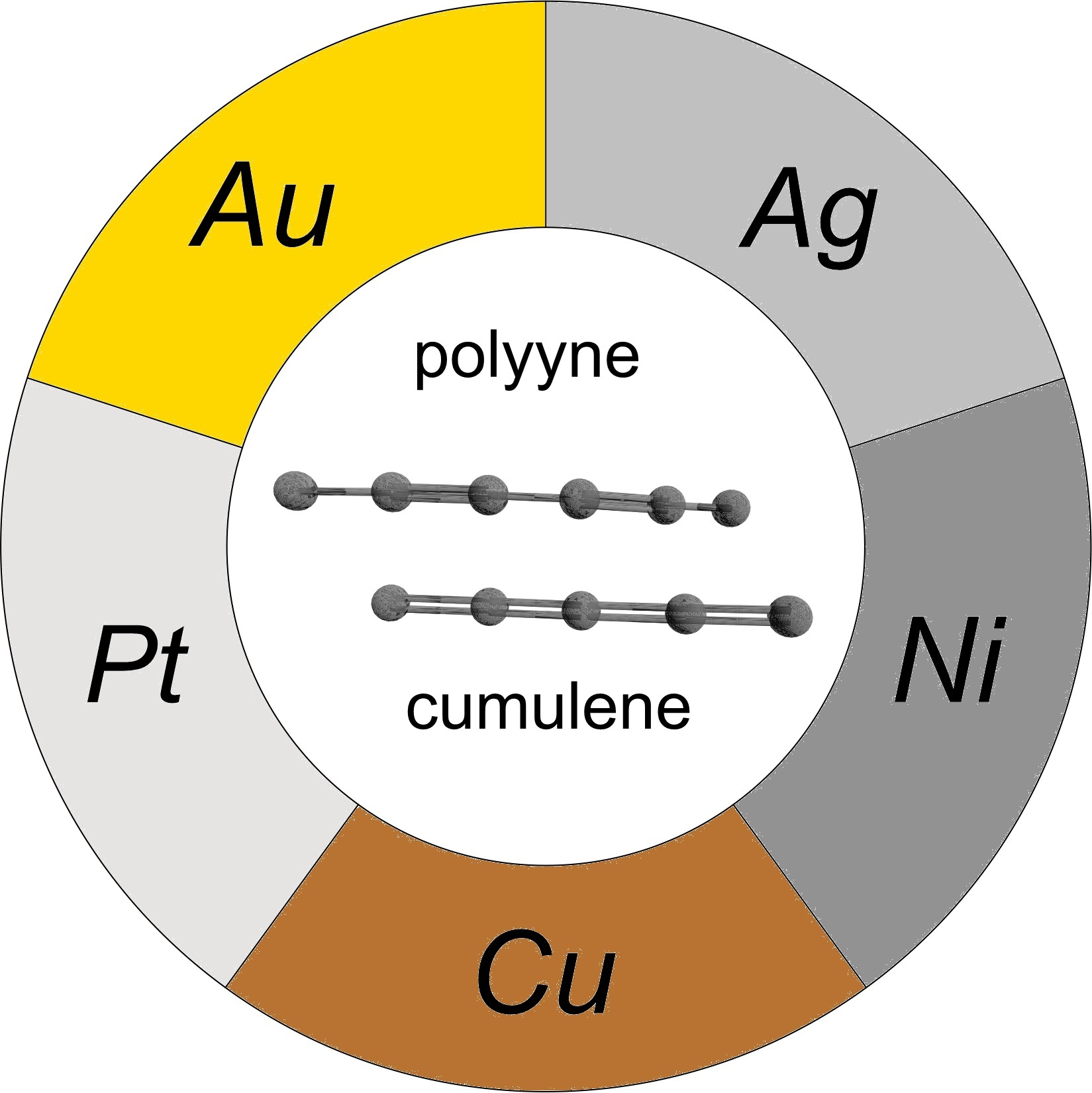
:
1. Introduction
2. Research Performed on Metal/Carbyne Interfaces
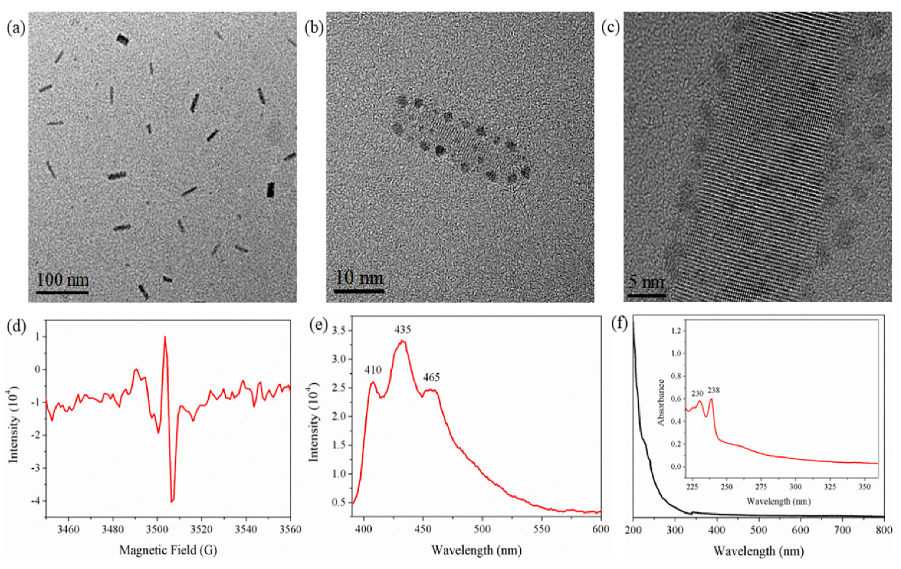
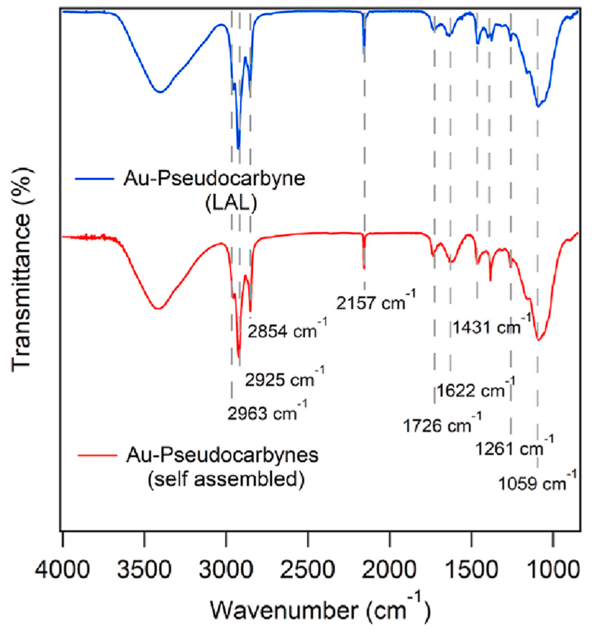
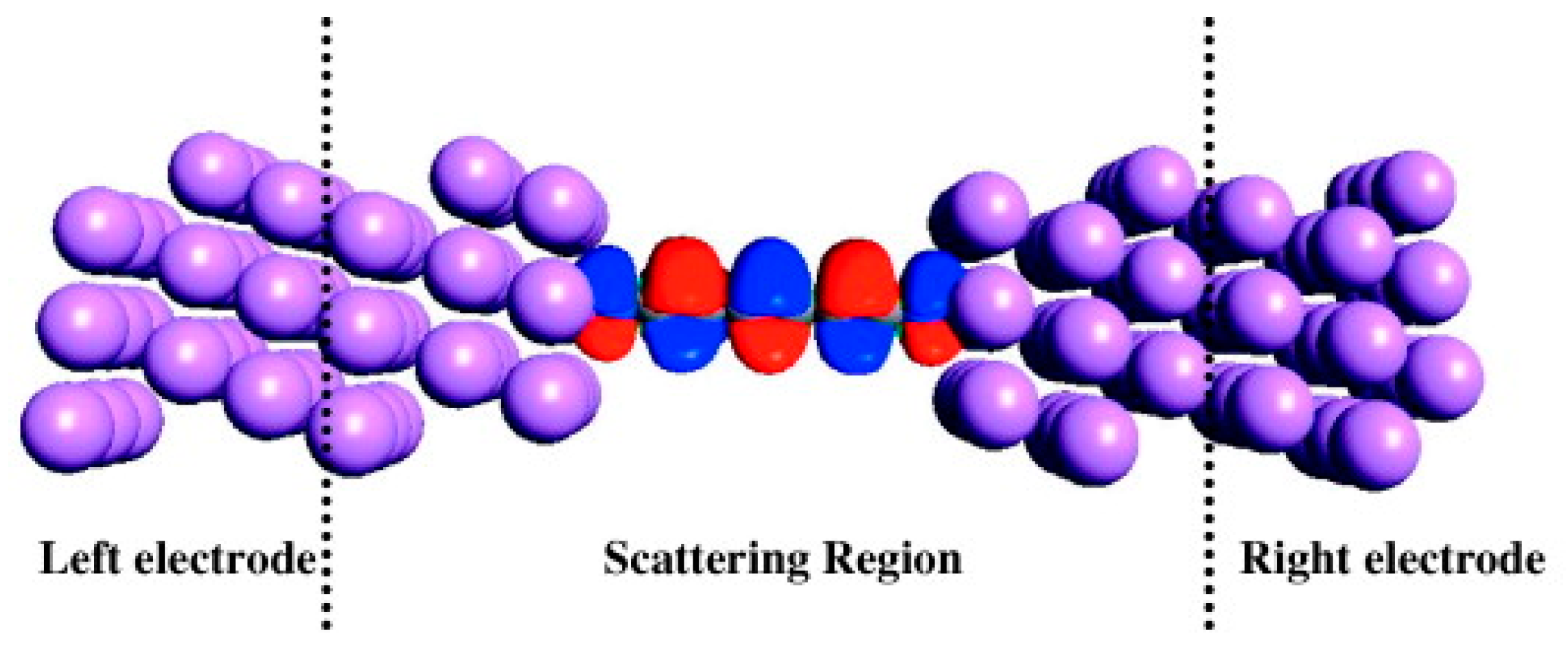
2.1. Research Performed on Au/Carbyne Interface
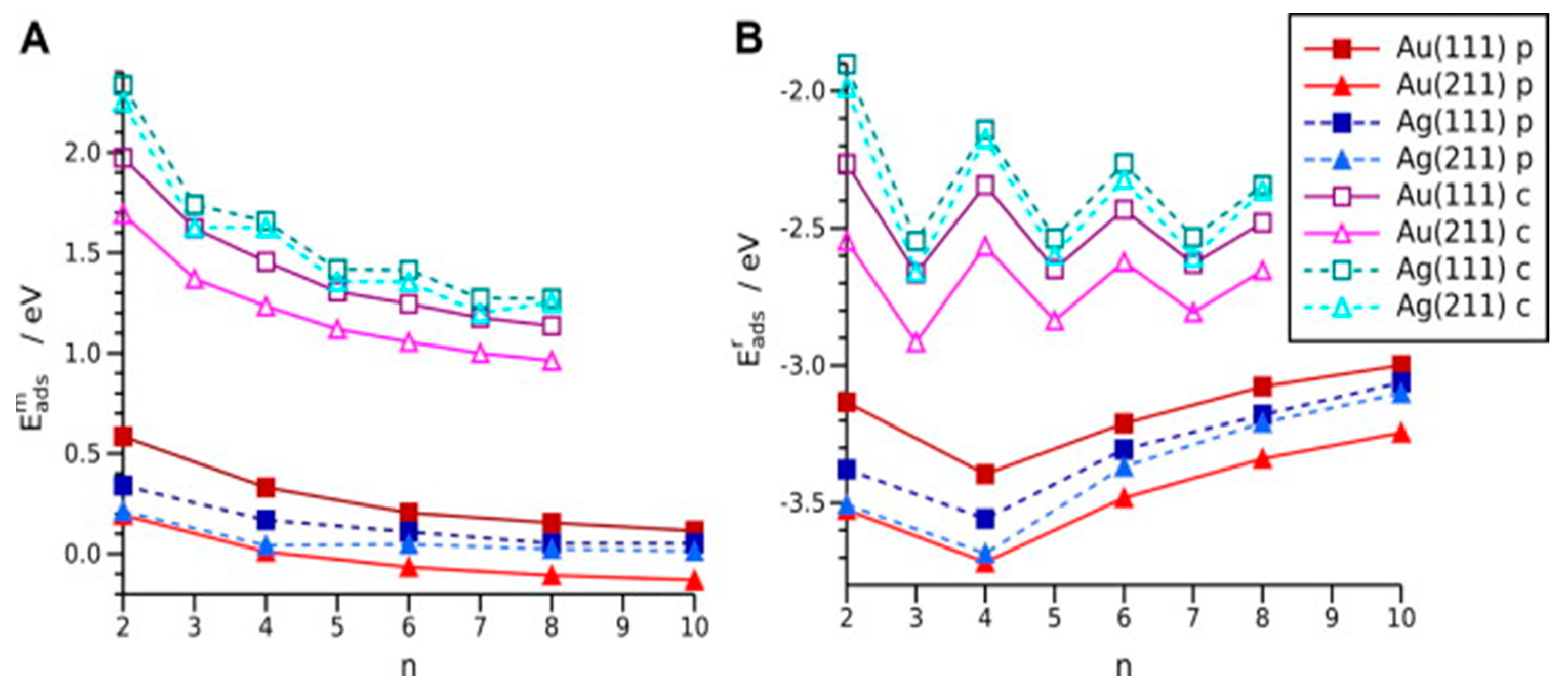
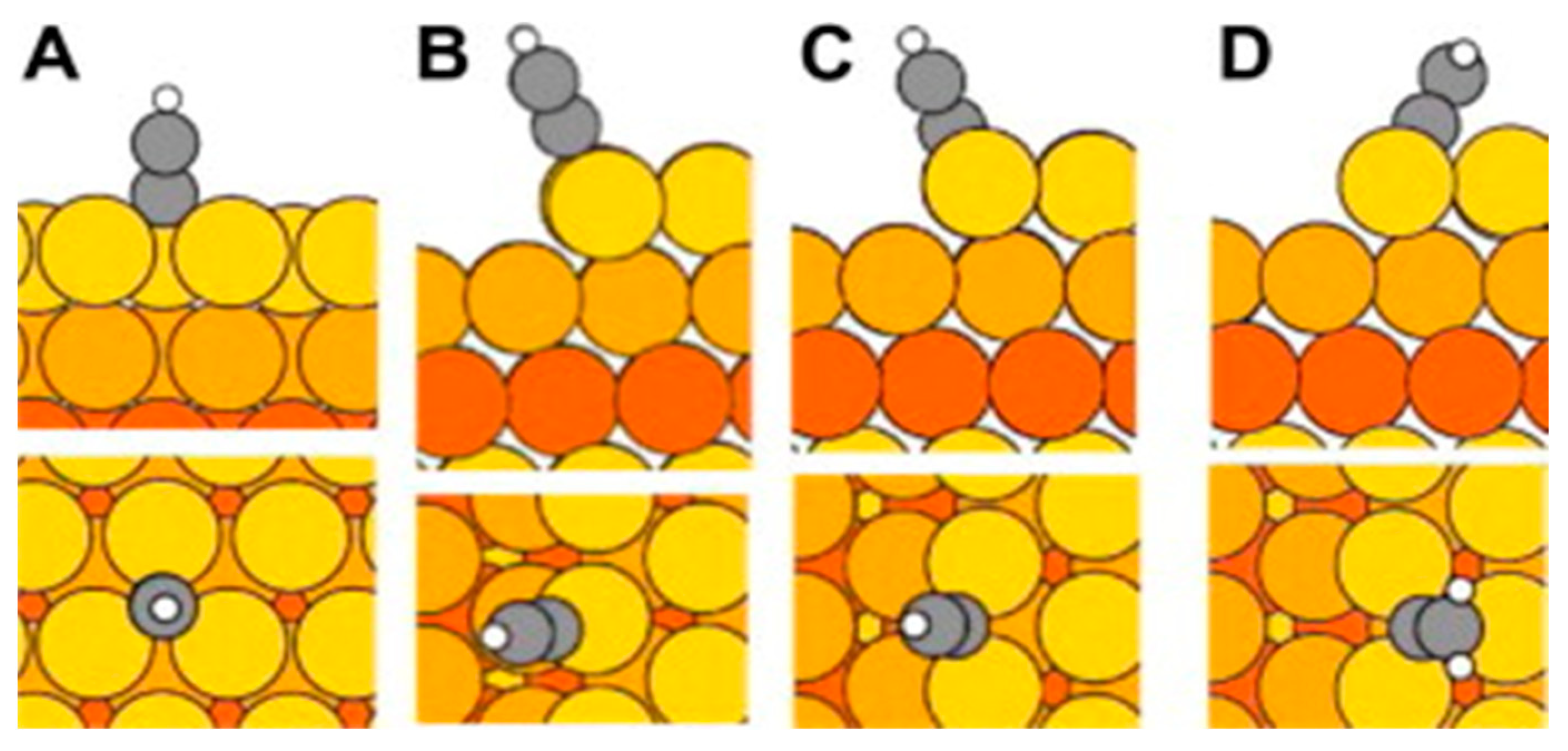
2.2. Research Performed on Ag/Carbyne Interface
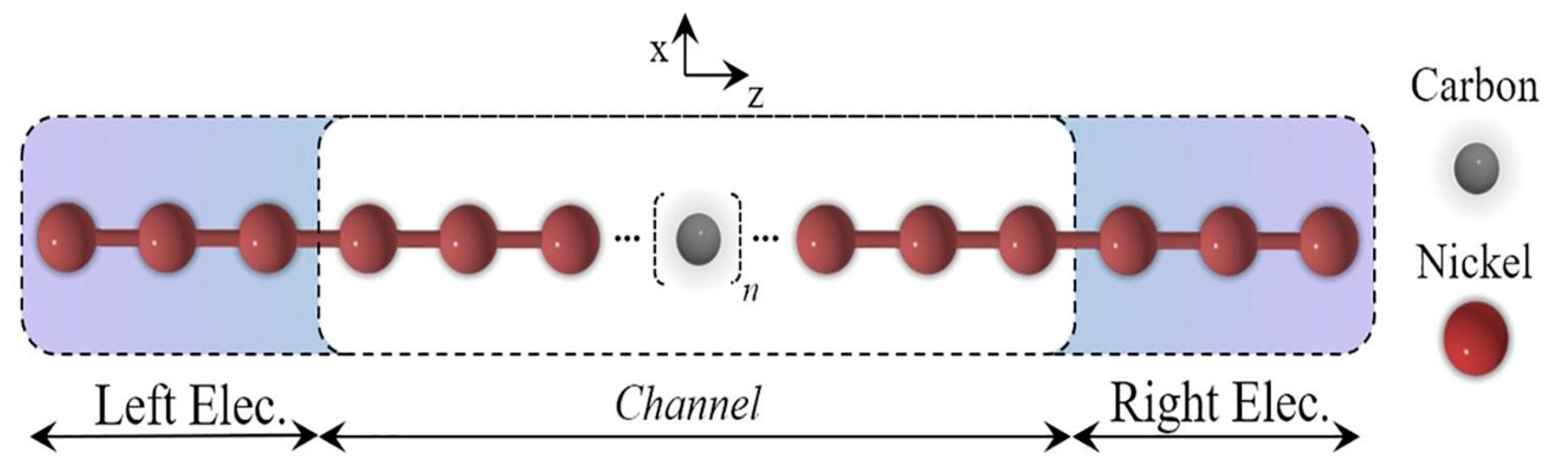
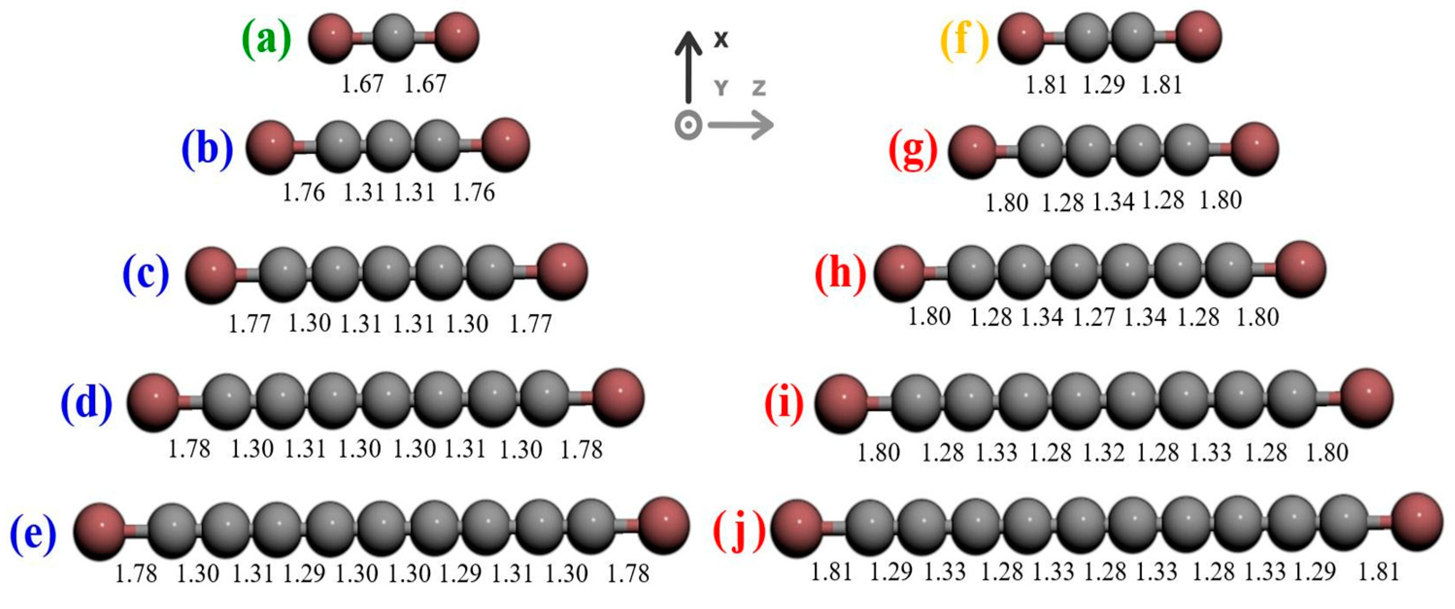
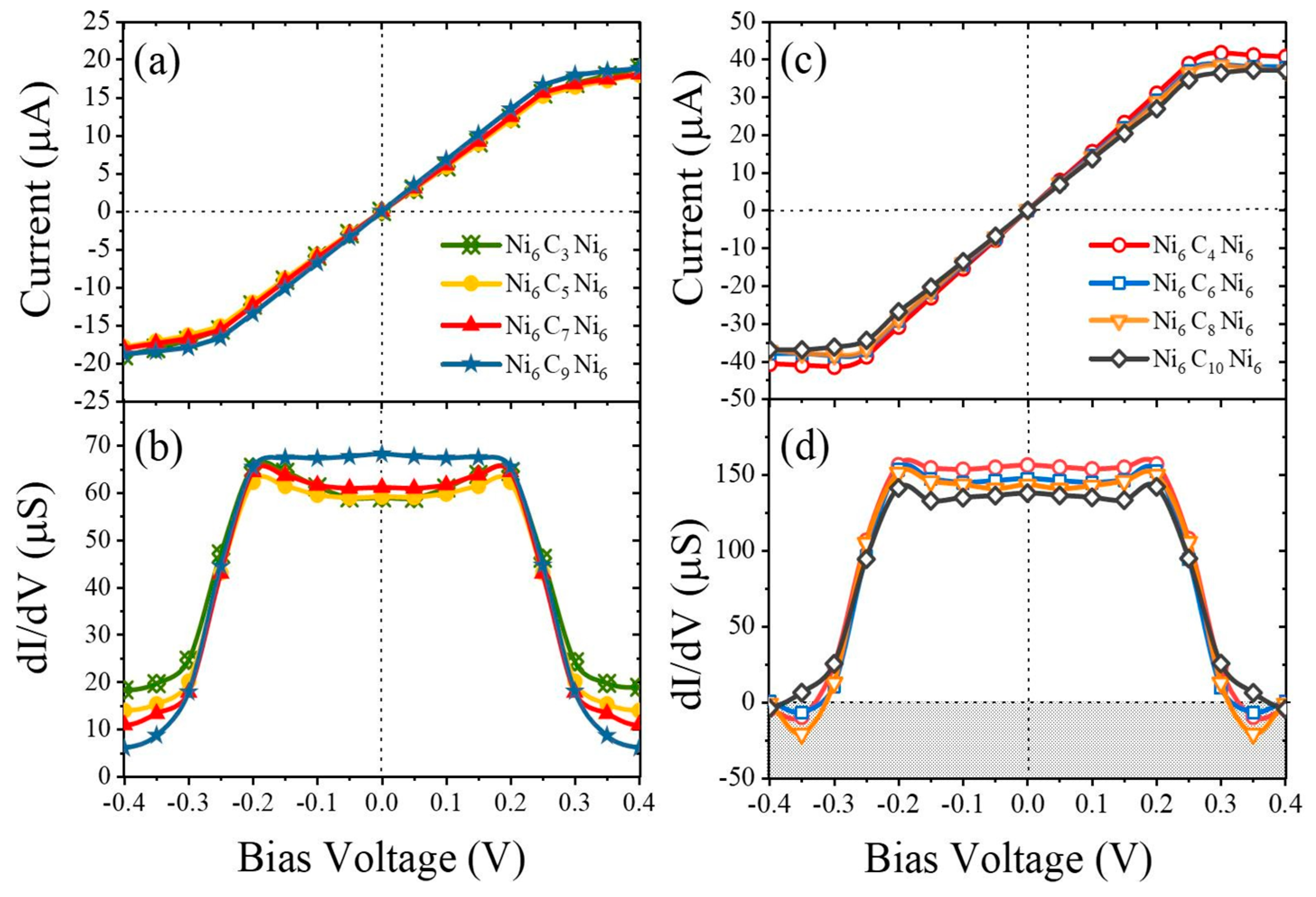
2.3. Research Performed on Ni/Carbyne Interface
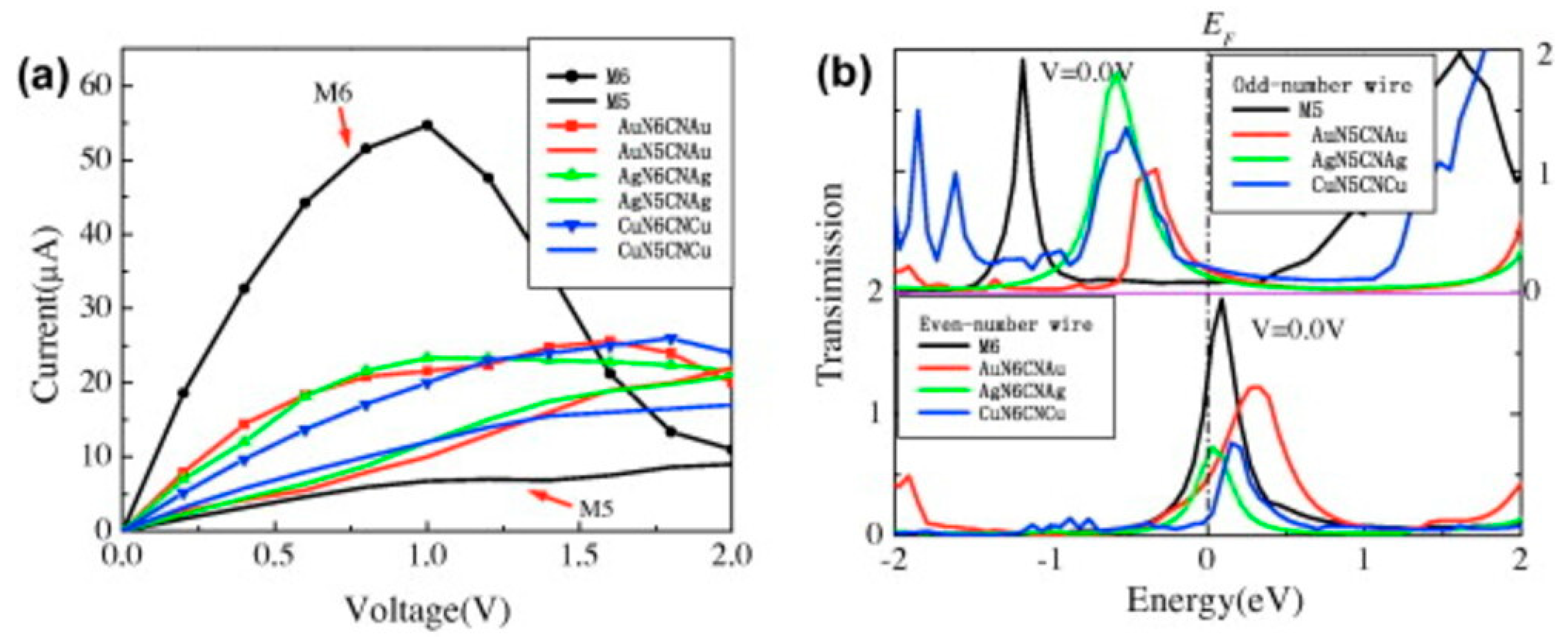
2.4. Research Performed on Cu/Carbyne Interface
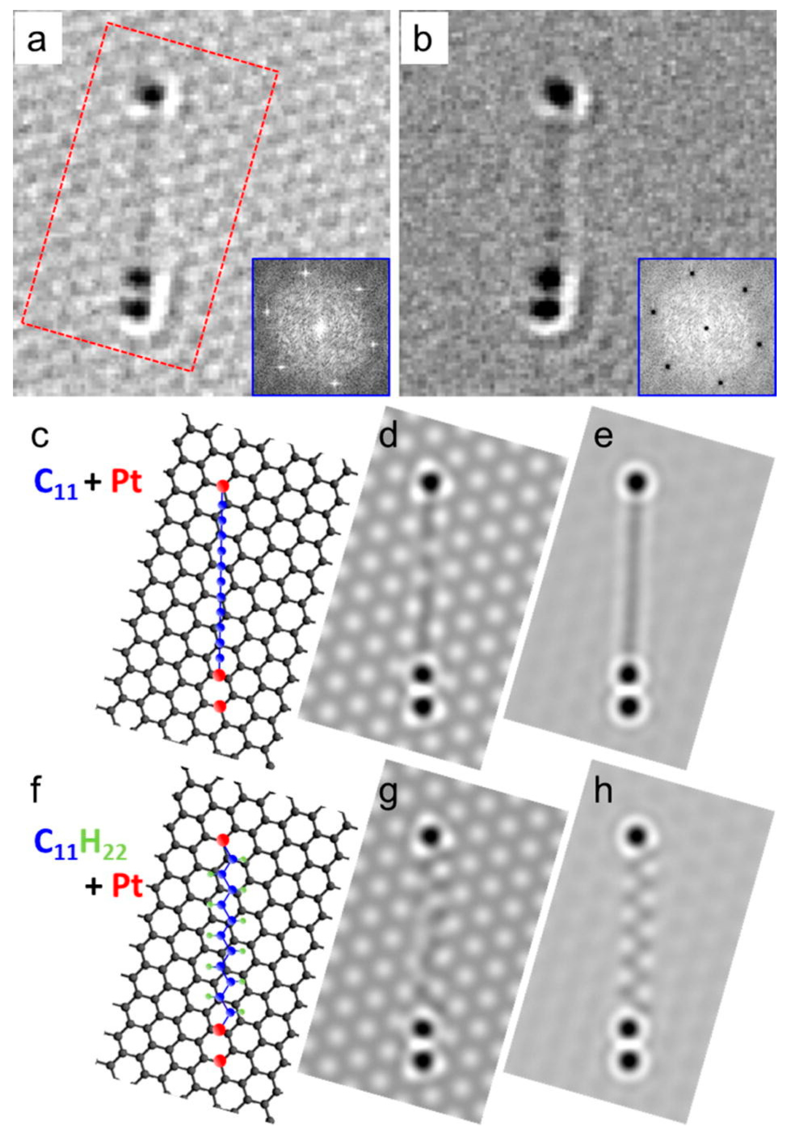
2.5. Research Performed on Pt/Carbyne Interface
3. Comparison of Systems with Different Metallization
4. Conclusions
Funding
Institutional Review Board Statement
Informed Consent Statement
Data Availability Statement
Conflicts of Interest
Sample Availability
References
- Jayan, K.D.; Sebastian, V. Comprehensive device modelling and performance analysis of MASnI3 based perovskite solar cells with diverse ETM, HTM and back metal contacts. Sol. Energy 2021, 217, 40–48. [Google Scholar] [CrossRef]
- Taleghani, N.M.; Heydari, Z.; Madani, M.; Nasiri, A.F.; Kolahdouz, M.; Abdy, H. Study of metal-Co/Zn-doped CuSCN contacts for efficient hole transport in perovskite solar cells. Opt. Mater. 2022, 133, 113009. [Google Scholar] [CrossRef]
- Xie, F.; Yang, M.; Jiang, M.; Huang, X.-J.; Liu, W.-Q.; Xie, P.-H. Carbon-based nanomaterials—A promising electrochemical sensor toward persistent toxic substance. TrAC Trends Anal. Chem. 2019, 119, 115624. [Google Scholar] [CrossRef]
- Le, T.; Priefer, R. Detection technologies of volatile organic compounds in the breath for cancer diagnoses. Talanta 2023, 265, 124767. [Google Scholar] [CrossRef] [PubMed]
- Nath, B.; Singh, S.; Behera, S.K.; Ramamurthy, P.C.; Mahapatra, D.R.; Hegde, G. Perovskite solar cell performance analysis via interface engineering employing MOF-composite. Sol. Energy 2023, 257, 249–256. [Google Scholar] [CrossRef]
- Kluska, S.; Bartsch, J.; Büchler, A.; Cimiotti, G.; Brand, A.A.; Hopman, S.; Glatthaar, M. Electrical and Mechanical Properties of Plated Ni/Cu Contacts for Si Solar Cells. Energy Procedia 2015, 77, 733–743. [Google Scholar] [CrossRef]
- Chakraborty, K.; Das, A.; Mandal, R.; Mandal, D. An analytical study on low voltage regime of natural organic semiconductor based device: Physics of trap energy and ideality factor. Solid State Commun. 2021, 323, 114080. [Google Scholar] [CrossRef]
- Yang, Y.; Pham, N.D.; Yao, D.; Zhu, H.; Yarlagadda, P.; Wang, H. Inorganic p-type semiconductors and carbon materials based hole transport materials for perovskite solar cells. Chin. Chem. Lett. 2018, 29, 1242–1250. [Google Scholar] [CrossRef]
- Liu, C.; Xu, Y.; Noh, Y.-Y. Contact engineering in organic field-effect transistors. Mater. Today 2015, 18, 79–96. [Google Scholar] [CrossRef]
- Szczęśniak, D.; Hoehn, R.D.; Kais, S. Canonical Schottky barrier heights of transition metal dichalcogenide monolayers in contact with a metal. Phys. Rev. B 2018, 97, 195315. [Google Scholar] [CrossRef]
- Zheng, Y.; Gao, J.; Han, C.; Chen, W. Ohmic Contact Engineering for Two-Dimensional Materials. Cell Rep. Phys. Sci. 2021, 2, 100298. [Google Scholar] [CrossRef]
- Yang, G. Synthesis, properties, and applications of carbyne nanocrystals. Mater. Sci. Eng. R Rep. 2022, 151, 100692. [Google Scholar] [CrossRef]
- Pan, B.; Xiao, J.; Li, J.; Liu, P.; Wang, C.; Yang, G. Carbyne with finite length: The one-dimensional sp carbon. Sci. Adv. 2015, 1, e1500857. [Google Scholar] [CrossRef] [PubMed]
- Neiss, C.; Trushin, E.; Görling, A. The Nature of One-Dimensional Carbon: Polyynic versus Cumulenic. ChemPhysChem 2014, 15, 2497–2502. [Google Scholar] [CrossRef]
- Nozaki, D.; Pastawski, H.M.; Cuniberti, G. Controlling the conductance of molecular wires by defect engineering. New J. Phys. 2010, 12, 063004. [Google Scholar] [CrossRef]
- Yang, F.; Zheng, Z.; Lin, Z.; Wang, B.; Liu, P.; Yang, G. Visible-light-driven room-temperature gas sensor based on carbyne nanocrystals. Sens. Actuators B Chem. 2020, 316, 128200. [Google Scholar] [CrossRef]
- Tomov, R.; Aleksandrova, M. Exploring Gold Contacts on Novel Carbyne-enriched Material. In Proceedings of the 46th In-ternational Spring Seminar on Electronics Technology (ISSE), Timisoara, Romania, 10–14 May 2023. [Google Scholar]
- Chen, T.; Yang, F.; Wu, X.; Chen, Y.; Yang, G. A fluorescent and colorimetric probe of carbyne nanocrystals coated Au nanoparticles for selective and sensitive detection of ferrous ions. Carbon 2020, 167, 196–201. [Google Scholar] [CrossRef]
- Kim, H.; Tarakeshwar, P.; Meneghetti, M.; Buseck, P.R.; Sayres, S.G. Formation of Au-pseudocarbynes by self-assembly of carbon chains and gold clusters. Carbon 2023, 205, 546–551. [Google Scholar] [CrossRef]
- Compagnini, G.; Patane, G.; D’Urso, L.; Puglisi, O.; Cataliotti, R.S.; Pignataro, B. On the Interaction of Carbon Nanowires with Noble Metals through a Study of Their Surface-Enhanced Raman Spectra. J. Phys. Chem. 2008, 112, 20301–20306. [Google Scholar] [CrossRef]
- Song, B.; Sanvito, S.; Fang, H. Anomalous I–V curve for mono-atomic carbon chains. New J. Phys. 2010, 12, 103017. [Google Scholar] [CrossRef]
- Zhang, Z.; Guo, C.; Kwong, G.; Deng, X. Electronic transport of nitrogen-capped monoatomic carbon wires between lithium electrodes. Carbon 2013, 51, 313–321. [Google Scholar] [CrossRef]
- Nykänen, L.; Häkkinen, H.; Honkala, K. Computational study of linear carbon chains on gold and silver surfaces. Carbon 2012, 50, 2752–2763. [Google Scholar] [CrossRef]
- Balakrishnan, A.; Shankar, R.; Vijayakumar, S. Polyyne-metal complexes for use in molecular wire applications: A DFT insight. Comput. Theor. Chem. 2021, 1202, 113328. [Google Scholar] [CrossRef]
- Cheng, Z.-L.; Skouta, R.; Vazquez, H.; Widawsky, J.R.; Schneebeli, S.; Chen, W.; Hybertsen, M.S.; Breslow, R.; Venkataraman, L. In situ formation of highly conducting covalent Au–C contacts for single-molecule junctions. Nat. Nanotechnol. 2011, 6, 353–357. [Google Scholar] [CrossRef]
- Chen, W.; Widawsky, J.R.; Vázquez, H.; Schneebeli, S.T.; Hybertsen, M.S.; Breslow, R.; Venkataraman, L. Highly Conducting π-Conjugated Molecular Junctions Covalently Bonded to Gold Electrodes. J. Am. Chem. Soc. 2011, 133, 17160–17163. [Google Scholar] [CrossRef]
- Fang, L.; Zhu, T.; Chang, W.; Liu, Y.; Zhao, X. Purification of polyynes via carbides. Carbon 2021, 179, 28–32. [Google Scholar] [CrossRef]
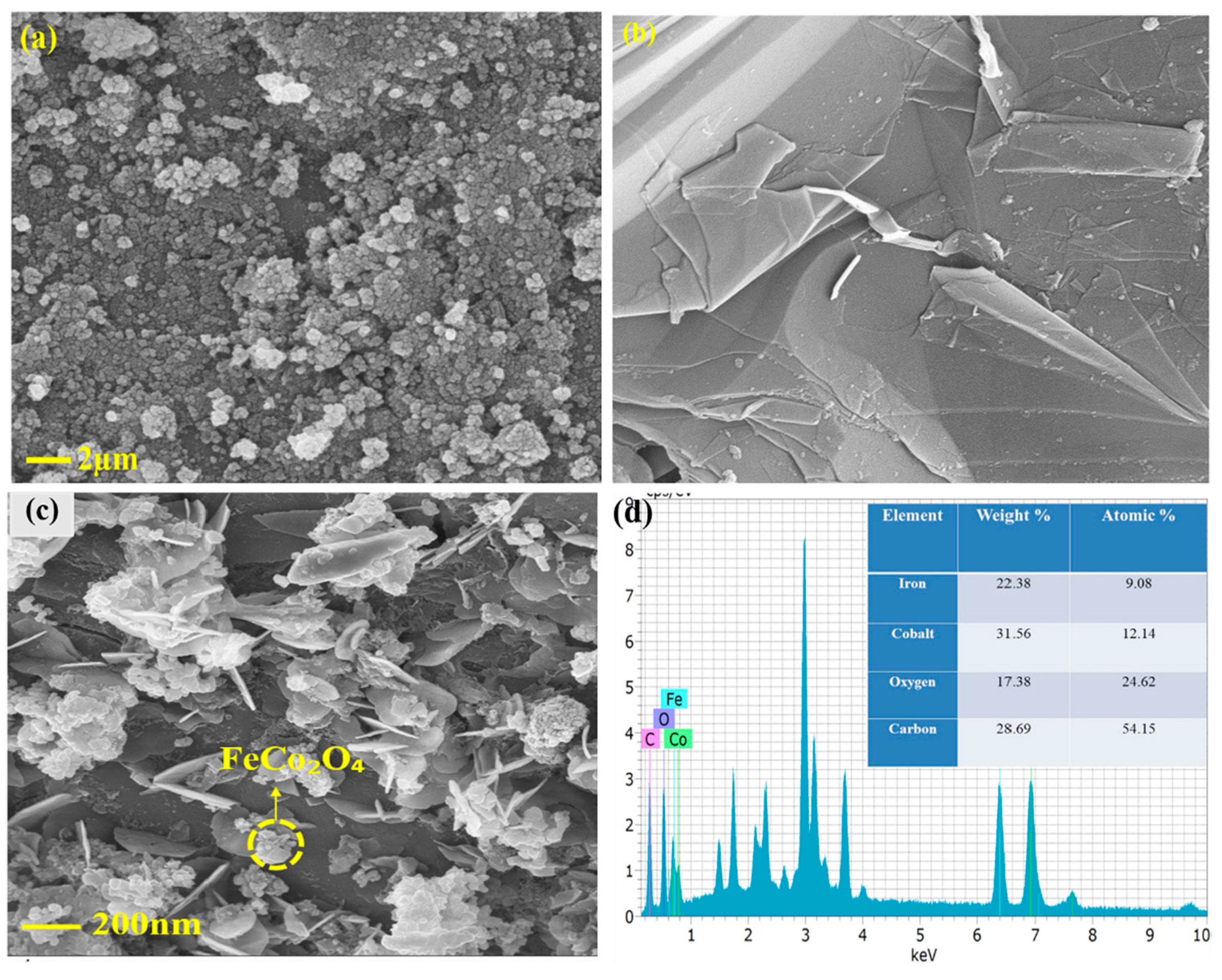
- Dhandapani, P.; Balan, B.; Dinadayalane, T.; Angaiah, S. In-situ grown of FeCo2O4 @ 2D-Carbyne coated nickel foam—A newer nanohybrid electrode for high performance asymmetric supercapacitors. J. Energy Storage 2022, 56, 105943. [Google Scholar] [CrossRef]
- Mariappan, V.K.; Krishnamoorthy, K.; Pazhamalai, P.; Sahoo, S.; Kim, S.-J. Carbyne-enriched carbon anchored on nickel foam: A novel binder-free electrode for supercapacitor application. J. Colloid Interface Sci. 2019, 556, 411–419. [Google Scholar] [CrossRef]
- Muller, S.E.; Nair, A.K. Carbyne as a fiber in metal-matrix nanocomposites: A first principle study. Comput. Mater. Sci. 2019, 159, 187–193. [Google Scholar] [CrossRef]
- Ferreira, D.F.S.; Moura-Moreira, M.; Corrêa, S.M.; da Silva, C.A.B., Jr.; Del Nero, J. Electronic transport in 1D system with coupling atomic-size nickel electrodes and carbon wires. Mater. Sci. Eng. B 2020, 262, 114681. [Google Scholar] [CrossRef]
- Pavlova, T.V.; Kovalenko, S.L.; Eltsov, K.N. Carbon chains and graphene nucleus synthesized on Ni(111) surface. arXiv 2017. [Google Scholar] [CrossRef]
- Sun, Q.; Cai, L.; Wang, S.; Widmer, R.; Ju, H.; Zhu, J.; Li, L.; He, Y.; Ruffieux, P.; Fasel, R.; et al. Bottom-Up Synthesis of Metalated Carbyne. J. Am. Chem. Soc. 2016, 138, 1106–1109. [Google Scholar] [CrossRef]
- Buntov, E.A.; Zatsepin, A.F.; Guseva, M.B.; Boqizoda, D.A.; Oksengendler, B.L. Structure and Raman scattering of chained carbon films on copper substrate: Ab initio approach. IOP Conf. Ser. Mater. Sci. Eng. 2018, 292, 012102. [Google Scholar] [CrossRef]
- Buntov, E.; Zatsepin, A.; Slesarev, A.; Shchapova, Y.; Challinger, S.; Baikie, I. Effect of thickness and substrate type on the structure and low vacuum photoemission of carbyne-containing films. Carbon 2019, 152, 388–395. [Google Scholar] [CrossRef]
- Cataldo, F. The role of Raman spectroscopy in the research on sp-hybridized carbon chains: Carbynoid structures polyynes and metal polyynides. J. Raman Spectrosc. 2008, 39, 169–176. [Google Scholar] [CrossRef]
- Cataldo, F.; Casari, C.S. Synthesis, Structure and Thermal Properties of Copper and Silver Polyynides and Acetylides. J. Inorg. Organomet. Polym. Mater. 2007, 17, 641–651. [Google Scholar] [CrossRef]
- Kano, E.; Takeguchi, M.; Fujita, J.-I.; Hashimoto, A. Direct observation of Pt-terminating carbyne on graphene. Carbon 2014, 80, 382–386. [Google Scholar] [CrossRef]
- Zhuravlev, F.; Gladysz, J.A. Electronic Structure and Chain-Length Effects in Diplatinum Polyynediyl Complexes trans,trans-[(X)(R3P)2Pt(C≡C)nPt(PR3)2(X)]: A Computational Investigation. Chem. Eur. J. 2004, 10, 6510–6522. [Google Scholar] [CrossRef] [PubMed]


| Metal | Au | Ag | Ni | Cu | Pt | |
|---|---|---|---|---|---|---|
| Bond length | Not reported | Not reported | x-odd 1.67 Å (x = 1) to 1.78 Å (x = 9) | x-even 1.81 Å | Not reported | 2.039 Å (x = 4) 2.031 Å (x = 26) |
| Raman peaks | 2130 cm−1 | 1985 cm−1 and 2117 cm−1. | Not reported | 1960 cm−1 and 2100 cm−1 | Not reported | |
Disclaimer/Publisher’s Note: The statements, opinions and data contained in all publications are solely those of the individual author(s) and contributor(s) and not of MDPI and/or the editor(s). MDPI and/or the editor(s) disclaim responsibility for any injury to people or property resulting from any ideas, methods, instructions or products referred to in the content. |
© 2023 by the authors. Licensee MDPI, Basel, Switzerland. This article is an open access article distributed under the terms and conditions of the Creative Commons Attribution (CC BY) license (https://creativecommons.org/licenses/by/4.0/).
Share and Cite
Tomov, R.; Aleksandrova, M. Overview of the Metallization Approaches for Carbyne-Based Devices. Molecules 2023, 28, 6409. https://doi.org/10.3390/molecules28176409
Tomov R, Aleksandrova M. Overview of the Metallization Approaches for Carbyne-Based Devices. Molecules. 2023; 28(17):6409. https://doi.org/10.3390/molecules28176409
Chicago/Turabian StyleTomov, Rade, and Mariya Aleksandrova. 2023. "Overview of the Metallization Approaches for Carbyne-Based Devices" Molecules 28, no. 17: 6409. https://doi.org/10.3390/molecules28176409
APA StyleTomov, R., & Aleksandrova, M. (2023). Overview of the Metallization Approaches for Carbyne-Based Devices. Molecules, 28(17), 6409. https://doi.org/10.3390/molecules28176409