
Electromagnetic Radiation Effects on MgO-Based Magnetic Tunnel Junctions: A Review


Abstract
1. Introduction
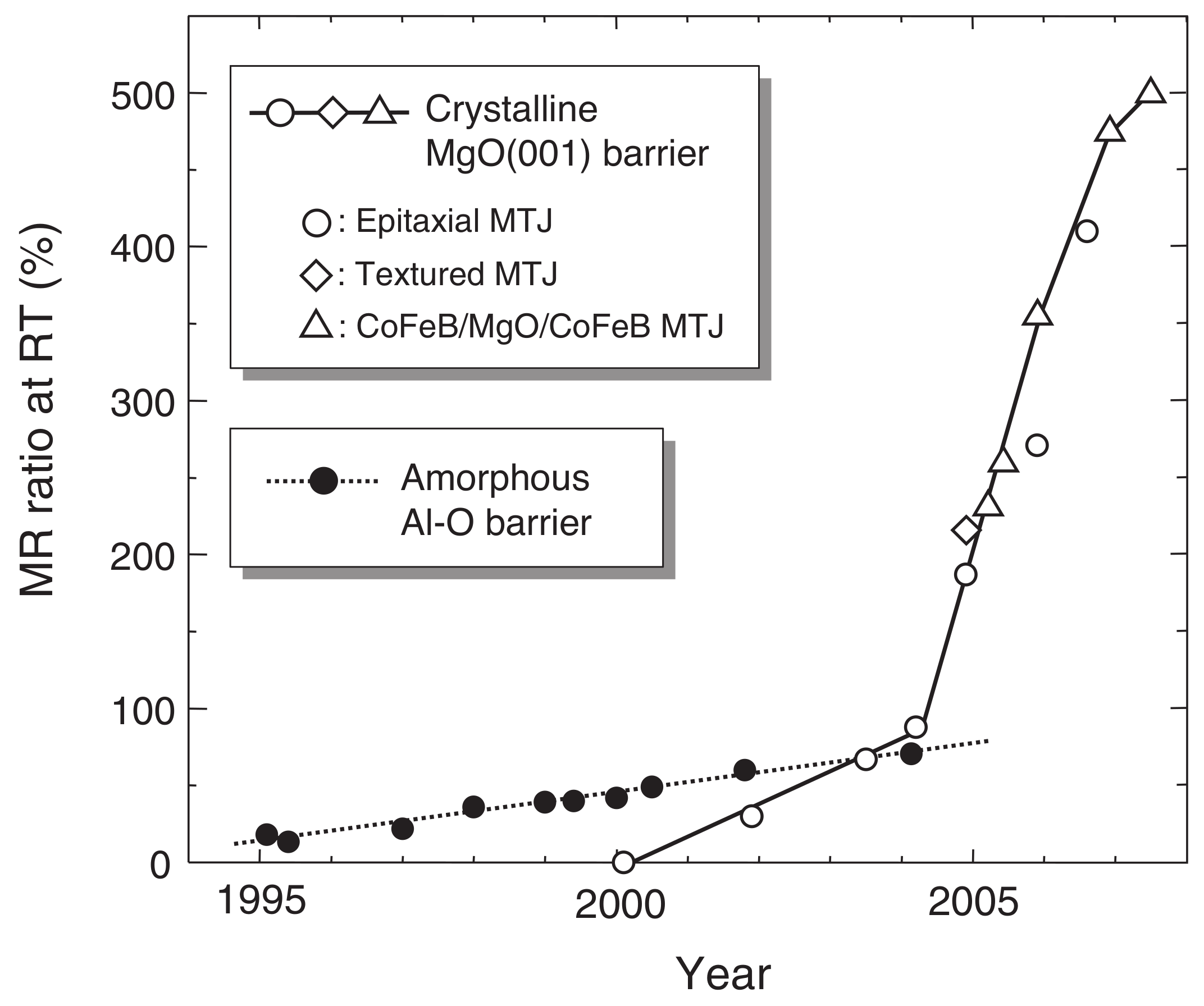
1.1. Tunnel Magnetoresistance
1.2. Applications of MTJs
1.2.1. Electronics
1.2.2. Energy Harvesting
1.2.3. Energy Storage
1.3. Irradiation
1.3.1. Natural Radiation Sources
1.3.2. Artificial Radiation Sources
1.3.3. Radiation Units
1.4. Properties of MTJ Materials
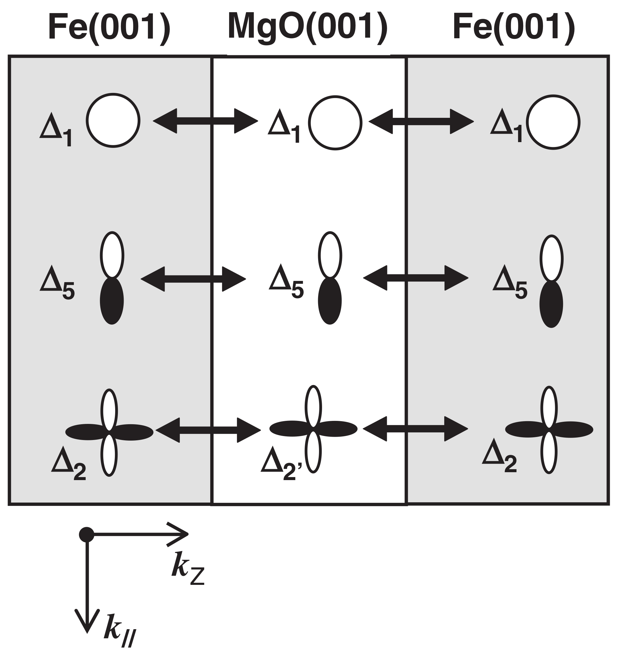
1.4.1. Magnesium Oxide Barrier
1.4.2. Ferromagnetic Layers
1.5. Theoretical Radiation Tolerance of MTJs
2. Effects of Cosmic Radiation
2.1. High-Energy Heavy-Ion Irradiation
2.2. High-Energy Proton Irradiation
2.3. High-Energy Neutron Irradiation
2.4. High-Energy Electron Irradiation
3. Effects of -ray Irradiation
3.1. MTJ Materials under -ray Irradiation
3.1.1. MgO Crystals under -ray Irradiation
3.1.2. Ferromagnetic Materials of MTJs under -ray Irradiation
3.1.3. Interfaces of MgO Barrier/Ferromagnetic Layers
3.2. MTJs under -ray Irradiation
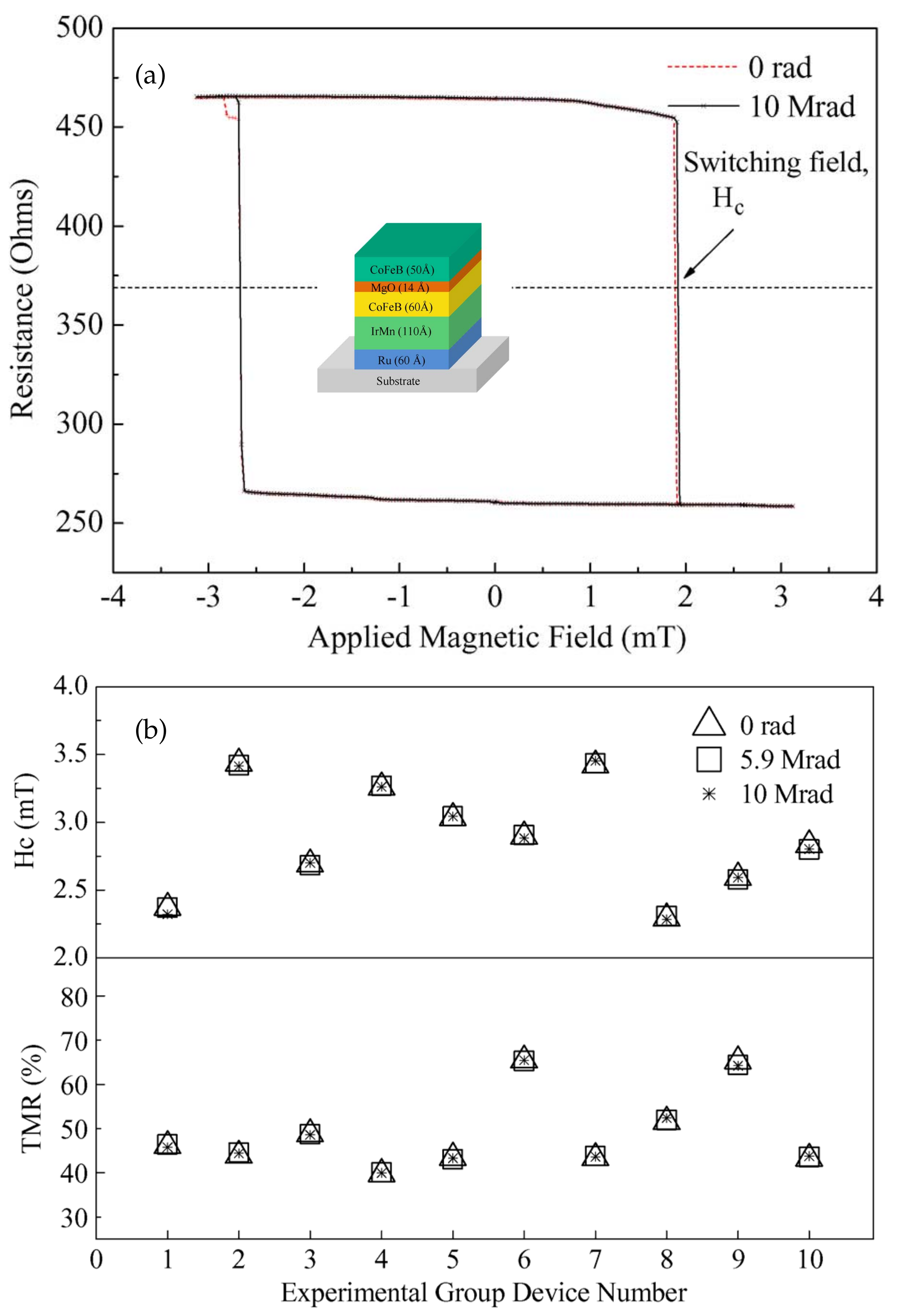
3.2.1. Sensitivity Results
3.2.2. Tolerance Results
3.3. Discussion of -ray Irradiation of MTJs
3.3.1. -ray Penetration in MTJs
3.3.2. Possible Explanations of Radiation Degradation
3.3.3. Possible Explanations of Tunneling Tolerance
3.3.4. Possible Explanations for Divergence
4. Effects of Lower-Energy Irradiation
4.1. X-ray Irradiation
4.2. UV–Vis Irradiation
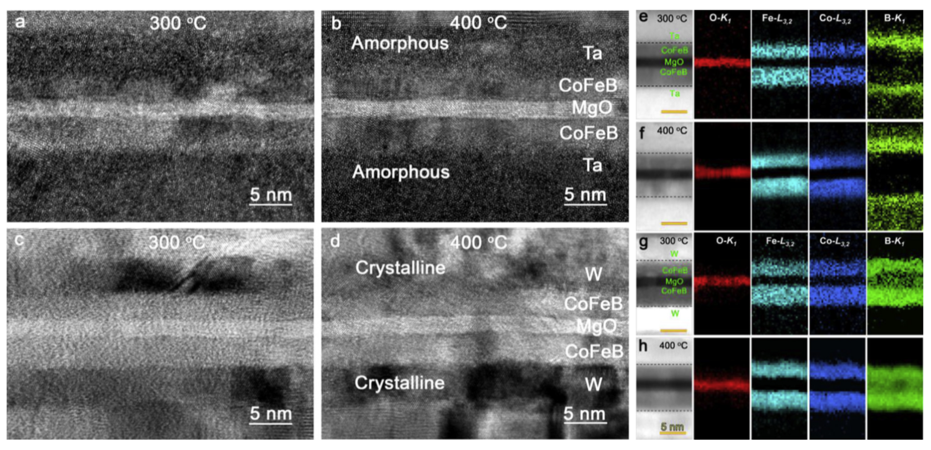
4.3. Infrared Radiation and Thermal Annealing
4.4. Microwave Irradiation
4.5. Radiofrequency Electromagnetic Irradiation
5. Outlook
6. Conclusions
Author Contributions
Funding
Institutional Review Board Statement
Informed Consent Statement
Data Availability Statement
Acknowledgments
Conflicts of Interest
Sample Availability
Abbreviations
| ADC | Analog-to-digital converter |
| AMR | Anisotropic magnetoresistance |
| CMOS | Complementary metal–oxide–semiconductor |
| DC | Direct current |
| DRAM | Dynamic random-access memory |
| GMR | Giant magnetoresistance |
| HDD | Hard disk drive |
| MOS | Metal oxide sensor |
| MR | Magnetoresistance |
| MRAM | Magnetic random-access memory |
| MTJ | Magnetic tunnel junction |
| PV | Photovoltaic |
| RAM | Random-access memory |
| RF | Radiofrequency |
| RT | Room temperature |
| SEM | Scanning electron microscopy |
| SRAM | Static random-access memory |
| TE | Thermoelectric |
| TEM | Transmission electron microscopy |
| TMR | Tunnel magnetoresistance |
References
- Wolf, S.A.; Awschalom, D.D.; Buhrman, R.A.; Daughton, J.M.; von Molnár, S.; Roukes, M.L.; Chtchelkanova, A.Y.; Treger, D.M. Spintronics: A spin-based electronics vision for the future. Science 2001, 294, 1488–1495. [Google Scholar] [CrossRef] [PubMed]
- Yuasa, S.; Nagahama, T.; Fukushima, A.; Suzuki, Y.; Ando, K. Giant room-temperature magnetoresistance in single-crystal Fe/MgO/Fe magnetic tunnel junctions. Nat. Mater. 2004, 3, 868–871. [Google Scholar] [CrossRef] [PubMed]
- Djayaprawira, D.D.; Tsunekawa, K.; Nagai, M.; Maehara, H.; Yamagata, S.; Watanabe, N.; Yuasa, S.; Suzuki, Y.; Ando, K. 230% room-temperature magnetoresistance in CoFeB/MgO/CoFeB magnetic tunnel junctions. Appl. Phys. Lett. 2005, 86, 092502. [Google Scholar] [CrossRef]
- Newman, A.; Khatiwada, S.; Neupane, S.; Seifu, D. Nanowires of Fe/multi-walled carbon nanotubes and nanometric thin films of Fe/MgO. J. Appl. Phys. 2015, 117, 144302. [Google Scholar] [CrossRef]
- Bowen, M.; Cros, V.; Petroff, F.; Fert, A.; Martínez Boubeta, C.; Costa-Krämer, J.L.; Anguita, J.V.; Cebollada, A.; Briones, F.; de Teresa, J.M.; et al. Large magnetoresistance in Fe/MgO/FeCo(001) epitaxial tunnel junctions on GaAs(001). Appl. Phys. Lett. 2001, 79, 1655–1657. [Google Scholar] [CrossRef]
- Bland, J.A.C.; Heinrich, B. Ultrathin Magnetic Structures I: An Introduction to the Electronic, Magnetic and Structural Properties; Springer Science & Business Media: Heidelberg, Germany, 1994. [Google Scholar]
- Gallagher, W.; Parkin, S. Development of the magnetic tunnel junction MRAM at IBM: From first junctions to a 16-Mb MRAM demonstrator chip. IBM J. Res. Dev. 2006, 50, 5–23. [Google Scholar] [CrossRef]
- Seifu, D. Nanowires of Fe/MgO/Fe encapsulated in carbon nanotubes. In Nanowires-Synthesis, Properties and Applications; IntechOpen: Rijeka, Hungary, 2018. [Google Scholar]
- Thomson, W. On the electro-dynamic qualities of metals: Effects of magnetization on the electric conductivity of nickel and of iron. Proc. R. Soc. Lond. 1856, 8, 546–550. [Google Scholar] [CrossRef]
- Nickel, J. Magnetoresistance overview. In HP Labs Technical Reports: HPL-95-60; Hewlett-Packard Company: Palo Alto, USA, 1995. [Google Scholar]
- McGuire, T.; Potter, R. Anisotropic magnetoresistance in ferromagnetic 3d alloys. IEEE Trans. Magn. 1975, 11, 1018–1038. [Google Scholar] [CrossRef]
- Baibich, M.N.; Broto, J.M.; Fert, A.; Van Dau, F.N.; Petroff, F.; Etienne, P.; Creuzet, G.; Friederich, A.; Chazelas, J. Giant magnetoresistance of (001)Fe/(001)Cr magnetic superlattices. Phys. Rev. Lett. 1988, 61, 2472–2475. [Google Scholar] [CrossRef]
- Binasch, G.; Grünberg, P.; Saurenbach, F.; Zinn, W. Enhanced magnetoresistance in layered magnetic structures with antiferromagnetic interlayer exchange. Phys. Rev. B 1989, 39, 4828–4830. [Google Scholar] [CrossRef]
- Camley, R.E.; Barnaś, J. Theory of giant magnetoresistance effects in magnetic layered structures with antiferromagnetic coupling. Phys. Rev. Lett. 1989, 63, 664–667. [Google Scholar] [CrossRef]
- Yuasa, S. Giant tunneling magnetoresistance in MgO-based magnetic tunnel junctions. J. Phys. Soc. Jpn. 2008, 77, 031001. [Google Scholar] [CrossRef]
- Zhu, J.G.; Park, C. Magnetic tunnel junctions. Mater. Today 2006, 9, 36–45. [Google Scholar] [CrossRef]
- Chappert, C.; Fert, A.; Van Dau, F.N. The emergence of spin electronics in data storage. Nat. Mater. 2007, 6, 813–823. [Google Scholar] [CrossRef] [PubMed]
- Jullière, M. Tunneling between ferromagnetic films. Phys. Lett. A 1975, 54, 225–226. [Google Scholar] [CrossRef]
- Miyazaki, T.; Tezuka, N. Giant magnetic tunneling effect in Fe/Al2O3/Fe junction. J. Magn. Magn. Mater. 1995, 139, L231–L234. [Google Scholar] [CrossRef]
- Yuasa, S.; Nagahama, T.; Suzuki, Y. Spin-polarized resonant tunneling in magnetic tunnel junctions. Science 2002, 297, 234–237. [Google Scholar] [CrossRef]
- Wang, D.; Nordman, C.; Daughton, J.; Qian, Z.; Fink, J. 70% TMR at room temperature for SDT sandwich junctions with CoFeB as free and reference layers. IEEE Trans. Magn. 2004, 40, 2269–2271. [Google Scholar] [CrossRef]
- Yuasa, S. Introduction to Magnetic Random-Access Memory; Chapter Magnetic Properties of Materials for MRAM; Wiley-Blackwell: Hoboken, NJ, USA, 2016; pp. 29–54. [Google Scholar] [CrossRef]
- Moodera, J.S.; Kinder, L.R. Ferromagnetic–insulator–ferromagnetic tunneling: Spin-dependent tunneling and large magnetoresistance in trilayer junctions (invited). J. Appl. Phys. 1996, 79, 4724–4729. [Google Scholar] [CrossRef]
- Faure-Vincent, J.; Tiusan, C.; Jouguelet, E.; Canet, F.; Sajieddine, M.; Bellouard, C.; Popova, E.; Hehn, M.; Montaigne, F.; Schuhl, A. High tunnel magnetoresistance in epitaxial Fe/MgO/Fe tunnel junctions. Appl. Phys. Lett. 2003, 82, 4507–4509. [Google Scholar] [CrossRef]
- Yuasa, S.; Fukushima, A.; Nagahama, T.; Ando, K.; Suzuki, Y. High tunnel magnetoresistance at room temperature in fully epitaxial Fe/MgO/Fe tunnel junctions due to coherent spin-polarized tunneling. Jpn. J. Appl. Phys. 2004, 43, L588. [Google Scholar] [CrossRef]
- Parkin, S.S.P.; Kaiser, C.; Panchula, A.; Rice, P.M.; Hughes, B.; Samant, M.; Yang, S.H. Giant tunnelling magnetoresistance at room temperature with MgO (100) tunnel barriers. Nat. Mater. 2004, 3, 862–867. [Google Scholar] [CrossRef] [PubMed]
- Ikeda, S.; Hayakawa, J.; Lee, Y.M.; Sasaki, R.; Meguro, T.; Matsukura, F.; Ohno, H. Dependence of tunnel magnetoresistance in MgO based magnetic tunnel junctions on Ar pressure during MgO sputtering. Jpn. J. Appl. Phys. 2005, 44, L1442. [Google Scholar] [CrossRef]
- Yuasa, S.; Fukushima, A.; Kubota, H.; Suzuki, Y.; Ando, K. Giant tunneling magnetoresistance up to 410 % at room temperature in fully epitaxial Co/MgO/Co magnetic tunnel junctions with bcc Co(001) electrodes. Appl. Phys. Lett. 2006, 89, 042505. [Google Scholar] [CrossRef]
- Lee, Y.M.; Hayakawa, J.; Ikeda, S.; Matsukura, F.; Ohno, H. Effect of electrode composition on the tunnel magnetoresistance of pseudo-spin-valve magnetic tunnel junction with a MgO tunnel barrier. Appl. Phys. Lett. 2007, 90, 212507. [Google Scholar] [CrossRef]
- Ikeda, S.; Hayakawa, J.; Ashizawa, Y.; Lee, Y.M.; Miura, K.; Hasegawa, H.; Tsunoda, M.; Matsukura, F.; Ohno, H. Tunnel magnetoresistance of 604% at 300K by suppression of Ta diffusion in CoFeB/MgO/CoFeB pseudo-spin-valves annealed at high temperature. Appl. Phys. Lett. 2008, 93, 082508. [Google Scholar] [CrossRef]
- Yuasa, S.; Djayaprawira, D.D. Giant tunnel magnetoresistance in magnetic tunnel junctions with a crystalline MgO(001) barrier. J. Phys. D: Appl. Phys. 2007, 40, R337. [Google Scholar] [CrossRef]
- Åkerman, J. Toward a Universal Memory. Science 2005, 308, 508–510. [Google Scholar] [CrossRef]
- Mao, S.; Chen, Y.; Liu, F.; Chen, X.; Xu, B.; Lu, P.; Patwari, M.; Xi, H.; Chang, C.; Miller, B.; et al. Commercial TMR heads for hard disk drives: Characterization and extendibility at 300Gbit/in2. IEEE Trans. Magn. 2006, 42, 97–102. [Google Scholar] [CrossRef]
- Puebla, J.; Kim, J.; Kondou, K.; Otani, Y. Spintronic devices for energy-efficient data storage and energy harvesting. Commun. Mater. 2020, 1, 24. [Google Scholar] [CrossRef]
- Hosomi, M.; Yamagishi, H.; Yamamoto, T.; Bessho, K.; Higo, Y.; Yamane, K.; Yamada, H.; Shoji, M.; Hachino, H.; Fukumoto, C.; et al. A novel nonvolatile memory with spin torque transfer magnetization switching: Spin-RAM. In Proceedings of the IEEE InternationalElectron Devices Meeting, 2005. IEDM Technical Digest, Washington, DC, USA, 5 December 2005; pp. 459–462. [Google Scholar] [CrossRef]
- Ho, M.; Tsang, C.; Fontana, R.E.; Parkin, S.; Carey, K.; Pan, T.; MacDonald, S.; Arnett, P.; Moore, J. Study of magnetic tunnel junction read sensors. IEEE Trans. Magn. 2001, 37, 1691–1694. [Google Scholar] [CrossRef]
- Mao, S.; Nowak, J.; Song, D.; Kolbo, P.; Wang, L.; Linville, E.; Saunders, D.; Murdock, E.; Ryan, P. Spin tunneling heads above 20Gb/in2. IEEE Trans. Magn. 2002, 38, 78–83. [Google Scholar] [CrossRef]
- Araki, S.; Sato, K.; Kagami, T.; Saruki, S.; Uesugi, T.; Kasahara, N.; Kuwashima, T.; Ohta, N.; Sun, J.; Nagai, K.; et al. Fabrication and electrical properties of lapped type of TMR heads for ∼50Gb/in2 and beyond. IEEE Trans. Magn. 2002, 38, 72–77. [Google Scholar] [CrossRef]
- Mao, S.; Linville, E.; Nowak, J.; Zhang, Z.; Chen, S.; Karr, B.; Anderson, P.; Ostrowski, M.; Boonstra, T.; Cho, H.; et al. Tunneling magnetoresistive heads beyond 150Gb/in2. IEEE Trans. Magn. 2004, 40, 307–312. [Google Scholar] [CrossRef]
- Kagami, T.; Kuwashima, T.; Miura, S.; Uesugi, T.; Barada, K.; Ohta, N.; Kasahara, N.; Sato, K.; Kanaya, T.; Kiyono, H.; et al. A performance study of next generation’s TMR heads beyond 200Gb/in2. IEEE Trans. Magn. 2006, 42, 93–96. [Google Scholar] [CrossRef]
- Horiguchi, F. Multi-Value Magnetic Random Access Memory with Stacked Tunnel Magnetoresistance (TMR) Elements. U.S. Patent 7,042,753, 9 May 2006. [Google Scholar]
- Tehrani, S.; Chen, E.; Durlam, M.; DeHerrera, M.; Slaughter, J.M.; Shi, J.; Kerszykowski, G. High density submicron magnetoresistive random access memory (invited). J. Appl. Phys. 1999, 85, 5822–5827. [Google Scholar] [CrossRef]
- Parkin, S.S.P.; Roche, K.P.; Samant, M.G.; Rice, P.M.; Beyers, R.B.; Scheuerlein, R.E.; O’Sullivan, E.J.; Brown, S.L.; Bucchigano, J.; Abraham, D.W.; et al. Exchange-biased magnetic tunnel junctions and application to nonvolatile magnetic random access memory (invited). J. Appl. Phys. 1999, 85, 5828–5833. [Google Scholar] [CrossRef]
- Tehrani, S.; Slaughter, J.; Chen, E.; Durlam, M.; Shi, J.; DeHerren, M. Progress and outlook for MRAM technology. IEEE Trans. Magn. 1999, 35, 2814–2819. [Google Scholar] [CrossRef]
- Engel, B.; Rizzo, N.; Janesky, J.; Slaughter, J.M.; Dave, R.; DeHerrera, M.; Durlam, M.; Tehrani, S. The science and technology of magnetoresistive tunneling memory. IEEE Trans. Nanotechnol. 2002, 1, 32–38. [Google Scholar] [CrossRef]
- Katti, R. Giant magnetoresistive random-access memories based on current-in-plane devices. Proc. IEEE 2003, 91, 687–702. [Google Scholar] [CrossRef]
- Tehrani, S.; Slaughter, J.M.; DeHerrera, M.; Engel, B.; Rizzo, N.; Salter, J.; Durlam, M.; Dave, R.; Janesky, J.; Butcher, B.; et al. Magnetoresistive random access memory using magnetic tunnel junctions. Proc. IEEE 2003, 91, 703–714. [Google Scholar] [CrossRef]
- Engel, B.; Åkerman, J.; Butcher, B.; Dave, R.; DeHerrera, M.; Durlam, M.; Grynkewich, G.; Janesky, J.; Pietambaram, S.; Rizzo, N.; et al. A 4-Mb toggle MRAM based on a novel bit and switching method. IEEE Trans. Magn. 2005, 41, 132–136. [Google Scholar] [CrossRef]
- Zhu, J.G. Magnetoresistive random access memory: The path to competitiveness and scalability. Proc. IEEE 2008, 96, 1786–1798. [Google Scholar] [CrossRef]
- Dave, R.; Steiner, G.; Slaughter, J.; Sun, J.; Craigo, B.; Pietambaram, S.; Smith, K.; Grynkewich, G.; DeHerrera, M.; Akerman, J.; et al. MgO-based tunnel junction material for high-speed toggle magnetic random access memory. IEEE Trans. Magn. 2006, 42, 1935–1939. [Google Scholar] [CrossRef]
- Gallagher, W.J.; Parkin, S.S.P.; Lu, Y.; Bian, X.P.; Marley, A.; Roche, K.P.; Altman, R.A.; Rishton, S.A.; Jahnes, C.; Shaw, T.M.; et al. Microstructured magnetic tunnel junctions (invited). J. Appl. Phys. 1997, 81, 3741–3746. [Google Scholar] [CrossRef]
- Gerardin, S.; Paccagnella, A. Present and future non-volatile memories for space. IEEE Trans. Nucl. Sci. 2010, 57, 3016–3039. [Google Scholar] [CrossRef]
- Jiang, Y.; Lv, Y.; Jamali, M.; Wang, J.P. Spin analog-to-digital convertor using magnetic tunnel junction and spin Hall effect. IEEE Electron. Device Lett. 2015, 36, 511–513. [Google Scholar] [CrossRef]
- Maciel, N.; Marques, E.; Naviner, L.; Cai, H. Magnetic tunnel junction-based analog-to-digital converter using spin orbit torque mechanism. In Proceedings of the 2020 27th IEEE International Conference on Electronics, Circuits and Systems (ICECS), Glasgow, UK, 23–25 November 2020; pp. 1–4. [Google Scholar] [CrossRef]
- Wu, Y.a.; Naviner, L.; Cai, H. Hybrid MTJ-CMOS integration for Sigma-Delta ADC. In Proceedings of the 2021 IEEE/ACM International Symposium on Nanoscale Architectures (NANOARCH), Virtual, 8–10 November 2021; pp. 1–5. [Google Scholar] [CrossRef]
- Paz, E.; Serrano-Guisan, S.; Ferreira, R.; Freitas, P.P. Room temperature direct detection of low frequency magnetic fields in the 100 pT/Hz0.5 range using large arrays of magnetic tunnel junctions. J. Appl. Phys. 2014, 115, 17E501. [Google Scholar] [CrossRef]
- Ferreira, R.; Wisniowski, P.; Freitas, P.P.; Langer, J.; Ocker, B.; Maass, W. Tuning of MgO barrier magnetic tunnel junction bias current for picotesla magnetic field detection. J. Appl. Phys. 2006, 99, 08K706. [Google Scholar] [CrossRef]
- Fan, X.; Cao, R.; Moriyama, T.; Wang, W.; Zhang, H.W.; Xiao, J.Q. Magnetic tunnel junction based microwave detector. Appl. Phys. Lett. 2009, 95, 122501. [Google Scholar] [CrossRef]
- Fan, X.; Chen, Y.; Bi, C.; Xie, Y.; Kolodzey, J.; Wilson, J.D.; Simons, R.N.; Zhang, H.; Xiao, J.Q. Magnetic tunnel junction-based on-chip microwave phase and spectrum analyzer. In Proceedings of the 2014 IEEE MTT-S International Microwave Symposium (IMS2014), Tampa, FL, USA, 1–6 June 2014; pp. 1–4. [Google Scholar] [CrossRef]
- Sengupta, A.; Liyanagedera, C.M.; Jung, B.; Roy, K. Magnetic tunnel junction as an on-chip Temperature Sensor. Sci. Rep. 2017, 7, 11764. [Google Scholar] [CrossRef] [PubMed]
- Bauer, G.E.W.; Saitoh, E.; van Wees, B.J. Spin caloritronics. Nat. Mater. 2012, 11, 391–399. [Google Scholar] [CrossRef] [PubMed]
- Otani, Y.; Shiraishi, M.; Oiwa, A.; Saitoh, E.; Murakami, S. Spin conversion on the nanoscale. Nat. Phys. 2017, 13, 829–832. [Google Scholar] [CrossRef]
- Johnson, I.; Choate, T.; Davidson, A. Waste Heat Recovery: Technology and Opportunities in U.S. Industry; Technical Report; BCS, Inc.: Aiken, SC, USA, 2008. [Google Scholar]
- Dresselhaus, M.S.; Chen, G.; Tang, M.Y.; Yang, R.G.; Lee, H.; Wang, D.Z.; Ren, Z.F.; Fleurial, J.P.; Gogna, P. New Directions for Low-Dimensional Thermoelectric Materials. Adv. Mater. 2007, 19, 1043–1053. [Google Scholar] [CrossRef]
- Poudel, B.; Hao, Q.; Ma, Y.; Lan, Y.; Minnich, A.; Yu, B.; Yan, X.; Wang, D.; Muto, A.; Vashaee, D.; et al. High-thermoelectric performance of nanostructured bismuth antimony telluride bulk alloys. Science 2008, 320, 634–638. [Google Scholar] [CrossRef] [PubMed]
- Lan, Y.C.; Wang, D.Z.; Chen, G.; Ren, Z.F. Diffusion of nickel and tin in p-type (Bi,Sb)2Te3 and n-type Bi2(Te,Se)3 thermoelectric materials. Appl. Phys. Lett. 2008, 92, 101910. [Google Scholar] [CrossRef]
- Lan, Y.; Poudel, B.; Ma, Y.; Wang, D.; Dresselhaus, M.S.; Chen, G.; Ren, Z. Structure study of bulk nanograined thermoelectric bismuth antimony telluride. Nano Lett. 2009, 9, 1419–1422. [Google Scholar] [CrossRef] [PubMed]
- Lan, Y.; Minnich, A.J.; Chen, G.; Ren, Z. Enhancement of thermoelectric figure-of-merit by a bulk nanostructuring approach. Adv. Func. Mater. 2010, 20, 357–376. [Google Scholar] [CrossRef]
- Liu, W.; Yan, X.; Chen, G.; Ren, Z. Recent advances in thermoelectric nanocomposites. Nano Energy 2012, 1, 42–56. [Google Scholar] [CrossRef]
- Ren, Z.; Lan, Y.; Zhang, Q. (Eds.) Advanced Thermoelectrics: Materials, Contacts, Modules, and Systems; CRC Press, Taylor and Francis Group: Boca Raton, FL, USA, 2017. [Google Scholar]
- Bao, X.; Hou, S.; Wu, Z.; Wang, X.; Yin, L.; Liu, Y.; He, H.; Duan, S.; Wang, B.; Mao, J.; et al. Mechanical properties of thermoelectric generators. J. Mater. Sci. Technol. 2023, 148, 64–74. [Google Scholar] [CrossRef]
- Liu, Z.; Gao, W.; Guo, F.; Cai, W.; Zhang, Q.; Sui, J. Challenges for Thermoelectric Power Generation: From a Material Perspective. Mater. Lab 2022, 1, 220003-1. [Google Scholar] [CrossRef]
- Mao, J.; Liu, Z.; Zhou, J.; Zhu, H.; Zhang, Q.; Chen, G.; Ren, Z. Advances in thermoelectrics. Adv. Phys. 2018, 67, 69–147. [Google Scholar] [CrossRef]
- Li, S.; Li, X.; Ren, Z.; Zhang, Q. Recent progress towards high performance of tin chalcogenide thermoelectric materials. J. Mater. Chem. A 2018, 6, 2432–2448. [Google Scholar] [CrossRef]
- Li, X.; Li, Z.; Chen, C.; Ren, Z.; Wang, C.; Liu, X.; Zhang, Q.; Chen, S. CALPHAD as a powerful technique for design and fabrication of thermoelectric materials as a powerful technique for design and fabrication of thermoelectric materials. J. Mater. Chem. A 2021, 9, 6634–6649. [Google Scholar] [CrossRef]
- Ren, W.; Shi, X.; Wang, Z.; Ren, Z. Crystallographic design for half-Heuslers with low lattice thermal conductivity. Mater. Today Phys. 2022, 25, 100704. [Google Scholar] [CrossRef]
- Jia, N.; Cao, J.; Tan, X.Y.; Dong, J.; Liu, H.; Tan, C.K.I.; Xu, J.; Yan, Q.; Loh, X.J.; Suwardi, A. Thermoelectric materials and transport physics. Mater. Today Phys. 2021, 21, 100519. [Google Scholar] [CrossRef]
- Basu, R.; Singh, A. High temperature Si-Ge alloy towards thermoelectric applications: A comprehensive review. Mater. Today Phys. 2021, 21, 100468. [Google Scholar] [CrossRef]
- Liu, W.; Hu, J.; Zhang, S.; Deng, M.; Han, C.-G.; Liu, Y. New trends, strategies and opportunities in thermoelectric materials: A perspective. Mater. Today Phys. 2017, 1, 50–60. [Google Scholar] [CrossRef]
- Shuai, J.; Mao, J.; Song, S.; Zhang, Q.; Chen, G.; Ren, Z. Recent progress and future challenges on thermoelectric Zintl materials. Mater. Today Phys. 2017, 1, 74–95. [Google Scholar] [CrossRef]
- Shan, J.; Dejene, F.K.; Leutenantsmeyer, J.C.; Flipse, J.; Münzenberg, M.; van Wees, B.J. Comparison of the magneto-Peltier and magneto-Seebeck effects in magnetic tunnel junctions. Phys. Rev. B 2015, 92, 020414. [Google Scholar] [CrossRef]
- Liebing, N.; Serrano-Guisan, S.; Krzysteczko, P.; Rott, K.; Reiss, G.; Langer, J.; Ocker, B.; Schumacher, H.W. Tunneling magneto thermocurrent in CoFeB/MgO/CoFeB based magnetic tunnel junctions. Appl. Phys. Lett. 2013, 102, 242413. [Google Scholar] [CrossRef]
- Liebing, N.; Serrano-Guisan, S.; Rott, K.; Reiss, G.; Langer, J.; Ocker, B.; Schumacher, H.W. Determination of spin-dependent Seebeck coefficients of CoFeB/MgO/CoFeB magnetic tunnel junction nanopillars. J. Appl. Phys. 2012, 111, 07C520. [Google Scholar] [CrossRef]
- Böhnert, T.; Dutra, R.; Sommer, R.L.; Paz, E.; Serrano-Guisan, S.; Ferreira, R.; Freitas, P.P. Influence of the thermal interface resistance on the thermovoltage of a magnetic tunnel junction. Phys. Rev. B 2017, 95, 104441. [Google Scholar] [CrossRef]
- Walter, M.; Walowski, J.; Zbarsky, V.; Münzenberg, M.; Schäfers, M.; Ebke, D.; Reiss, G.; Thomas, A.; Peretzki, P.; Seibt, M.; et al. Seebeck effect in magnetic tunnel junctions. Nat. Mater. 2011, 10, 742–746. [Google Scholar] [CrossRef] [PubMed]
- Boehnke, A.; Walter, M.; Roschewsky, N.; Eggebrecht, T.; Drewello, V.; Rott, K.; Münzenberg, M.; Thomas, A.; Reiss, G. Time-resolved measurement of the tunnel magneto-Seebeck effect in a single magnetic tunnel junction. Rev. Sci. Instrum. 2013, 84, 063905. [Google Scholar] [CrossRef]
- Huebner, T.; Boehnke, A.; Martens, U.; Thomas, A.; Schmalhorst, J.M.; Reiss, G.; Münzenberg, M.; Kuschel, T. Comparison of laser-induced and intrinsic tunnel magneto-Seebeck effect in CoFeB/MgAl2O4 and CoFeB/MgO magnetic tunnel junctions. Phys. Rev. B 2016, 93, 224433. [Google Scholar] [CrossRef]
- Lin, W.; Hehn, M.; Chaput, L.; Negulescu, B.; Andrieu, S.; Montaigne, F.; Mangin, S. Giant spin-dependent thermoelectric effect in magnetic tunnel junctions. Nat. Commun. 2012, 3, 744. [Google Scholar] [CrossRef]
- Liebing, N.; Serrano-Guisan, S.; Rott, K.; Reiss, G.; Langer, J.; Ocker, B.; Schumacher, H.W. Tunneling magnetothermopower in magnetic tunnel junction nanopillars. Phys. Rev. Lett. 2011, 107, 177201. [Google Scholar] [CrossRef]
- Böhnert, T.; Paz, E.; Ferreira, R.; Freitas, P.P. Magnetic tunnel junction thermocouple for thermoelectric power harvesting. Phys. Lett. A 2018, 382, 1437–1440. [Google Scholar] [CrossRef]
- Ellsworth, D.; Lu, L.; Lan, J.; Chang, H.; Li, P.; Wang, Z.; Hu, J.; Johnson, B.; Bian, Y.; Xiao, J.; et al. Photo-spin-voltaic effect. Nat. Phys. 2016, 12, 861–866. [Google Scholar] [CrossRef]
- Weiler, M.; Huebl, H.; Goerg, F.S.; Czeschka, F.D.; Gross, R.; Goennenwein, S.T.B. Spin pumping with coherent elastic waves. Phys. Rev. Lett. 2012, 108, 176601. [Google Scholar] [CrossRef] [PubMed]
- Xu, M.; Puebla, J.; Auvray, F.; Rana, B.; Kondou, K.; Otani, Y. Inverse Edelstein effect induced by magnon-phonon coupling. Phys. Rev. B 2018, 97, 180301. [Google Scholar] [CrossRef]
- Gui, Y.S.; Xiao, Y.; Bai, L.H.; Hemour, S.; Zhao, Y.P.; Houssameddine, D.; Wu, K.; Guo, H.; Hu, C.M. High sensitivity microwave detection using a magnetic tunnel junction in the absence of an external applied magnetic field. Appl. Phys. Lett. 2015, 106, 152403. [Google Scholar] [CrossRef]
- Kaiju, H.; Fujita, S.; Morozumi, T.; Shiiki, K. Magnetocapacitance effect of spin tunneling junctions. J. Appl. Phys. 2002, 91, 7430–7432. [Google Scholar] [CrossRef]
- Kaiju, H.; Takei, M.; Misawa, T.; Nagahama, T.; Nishii, J.; Xiao, G. Large magnetocapacitance effect in magnetic tunnel junctions based on Debye-Fröhlich model. Appl. Phys. Lett. 2015, 107, 132405. [Google Scholar] [CrossRef]
- Kaiju, H.; Misawa, T.; Nagahama, T.; Komine, T.; Kitakami, O.; Fujioka, M.; Nishii, J.; Xiao, G. Robustness of voltage-induced magnetocapacitance. Sci. Rep. 2018, 8, 14709. [Google Scholar] [CrossRef]
- Kaiju, H.; Nagahama, T.; Sasaki, S.; Shimada, T.; Kitakami, O.; Misawa, T.; Fujioka, M.; Nishii, J.; Xiao, G. Inverse tunnel magnetocapacitance in Fe/Al-oxide/Fe3O4. Sci. Rep. 2017, 7, 2682. [Google Scholar] [CrossRef] [PubMed]
- Lee, T.H.; Chen, C.D. Probing spin accumulation induced magnetocapacitance in a single electron transistor. Sci. Rep. 2015, 5, 13704. [Google Scholar] [CrossRef]
- Sato, K.; Sukegawa, H.; Ogata, K.; Xiao, G.; Kaiju, H. Large magnetocapacitance beyond 420% in epitaxial magnetic tunnel junctions with an MgAl2O4 barrier. Sci. Rep. 2022, 12, 7190. [Google Scholar] [CrossRef]
- Hai, P.N.; Ohya, S.; Tanaka, M.; Barnes, S.E.; Maekawa, S. Electromotive force and huge magnetoresistance in magnetic tunnel junctions. Nature 2009, 458, 489–492. [Google Scholar] [CrossRef]
- Grieder, P.K.F. Cosmic Rays at Earth: Researcher’s Reference Manual and Data Book; Elsevier Science: Amsterdam, The Netherlands, 2001; ISBN 9780444507105. [Google Scholar]
- Natural Space Radiation Effects on Technology. Available online: https://radhome.gsfc.nasa.gov/radhome/nat_space_rad_tech.htm (accessed on 11 May 2023).
- Baumann, R.; Kruckmeyer, K. Radiation Handbook for Electronics: A Compendium of Radiation Effects Topics for Space, Industrial and Terrestrial Applications; Texas Instruments: Dallas, TX, USA, 2020. [Google Scholar]
- Haynes, W.M. (Ed.) CRC Handbook of Chemistry and Physics, 92nd ed.; CRC Press: Boca Raton, FL, USA, 2011. [Google Scholar]
- Vollmer, M. Physics of the microwave oven. Phys. Educ. 2004, 39, 74–81. [Google Scholar] [CrossRef]
- GSM frequency Bands. Available online: https://en.wikipedia.org/wiki/GSM_frequency_bands (accessed on 11 May 2023).
- Cellular frequencies in the United States. Available online: https://en.wikipedia.org/wiki/Cellular_frequencies_in_the_United_States (accessed on 11 May 2023).
- 5G. Available online: https://en.wikipedia.org/wiki/5G (accessed on 11 May 2023).
- An, S.; Shang, W.; Jiang, M.; Luo, Y.; Fu, B.; Song, C.; Tao, P.; Deng, T. Human hand as a powerless and multiplexed infrared light source for information decryption and complex signal generation. Proc. Natl. Acad. Sci. USA 2021, 118, e2021077118. [Google Scholar] [CrossRef] [PubMed]
- Elghefari, M.; McClure, S. Radiation Effects Assessment of MRAM Devices; Technical Report; Jet Propulsion Laboratory: Pasadena, CA, USA, 2008. [Google Scholar]
- Zhao, G.Y.; Deng, H.; Tyree, N.; Guy, M.; Lisfi, A.; Peng, Q.; Yan, J.A.; Wang, C.; Lan, Y. Recent Progress on Irradiation-Induced Defect Engineering of Two-Dimensional 2H-MoS2 Few Layers. Appl. Sci. 2019, 9, 678. [Google Scholar] [CrossRef]
- Pomeroy, J.; Grube, H.; Perrella, A.; Gillaspy, J. STM and transport measurements of highly charged ion modified materials. Nucl. Instrum. Meth. B 2007, 258, 189–193. [Google Scholar] [CrossRef]
- Kobayashi, D.; Kakehashi, Y.; Hirose, K.; Onoda, S.; Makino, T.; Ohshima, T.; Ikeda, S.; Yamanouchi, M.; Sato, H.; Enobio, E.C.; et al. Influence of heavy ion irradiation on perpendicular-anisotropy CoFeB-MgO magnetic tunnel junctions. IEEE Trans. Nucl. Sci. 2014, 61, 1710–1716. [Google Scholar] [CrossRef]
- Cost, J.; Brown, R.; Giorgi, A.; Stanley, J. Effects of neutron irradiation on Nd-Fe-B magnetic properties. IEEE Trans. Magnet. 1988, 24, 2016–2019. [Google Scholar] [CrossRef]
- Liu, B.; Tahmasebi, T.; Ong, K.; Teo, H.; Mo, Z.; Lam, J.; Tan, P.K.; Zhao, Y.; Dong, Z.; Houssameddine, D.; et al. Electron radiation-induced material diffusion and nanocrystallization in nanostructured amorphous CoFeB thin film. Acta Mater. 2018, 161, 221–236. [Google Scholar] [CrossRef]
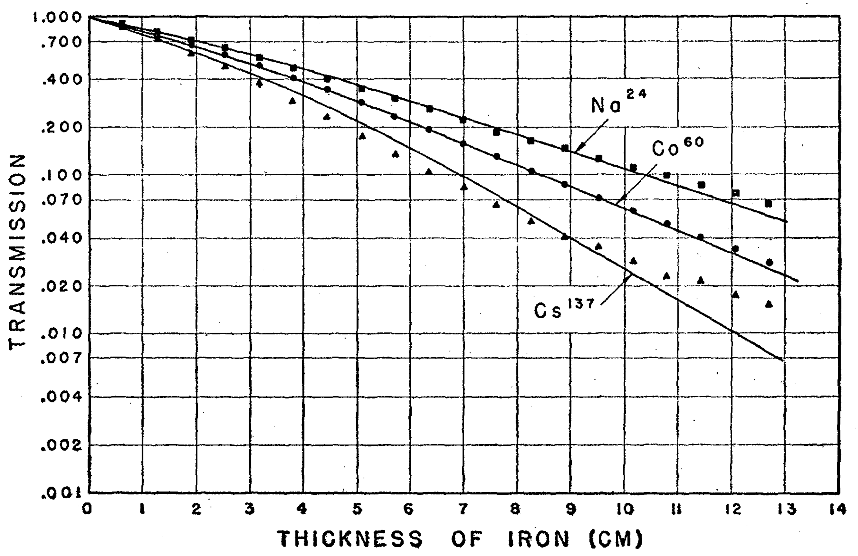
- Beach, L.A.; Theus, R.B.; Faust, W.R. Penetration of gamma radiation through iron. Phys. Rev. 1953, 92, 355. [Google Scholar] [CrossRef]
- Shkapa, V.M.; Shalaev, A.M.; Polotnjuk, V.V.; Likhtorovich, S.P.; Nemoshkalenko, V.V.; Kotov, V.V. Positron, Mössbauer and NMR studies of γ-irradiated FeCoB metallic glasses. J. Non. Cryst. Solids 1993, 155, 90–94. [Google Scholar] [CrossRef]
- Hughes, H.; Bussmann, K.; McMarr, P.J.; Cheng, S.; Shull, R.; Chen, A.P.; Schafer, S.; Mewes, T.; Ong, A.; Chen, E.; et al. Radiation studies of spin-transfer torque materials and devices. IEEE Trans. Nucl. Sci. 2012, 59, 3027–3033. [Google Scholar] [CrossRef]
- Wang, B.; Wang, Z.; Cao, K.; Bi, X.; Zhao, Y.; Zhang, Y.; Zhao, W. Effects of gamma irradiation on magnetic properties of double-interface CoFeB/MgO multifilms. IEEE Trans. Nucl. Sci. 2019, 66, 77–81. [Google Scholar] [CrossRef]
- Arshak, K.; Morris, D.; Kaneswaran, K.; Korostynska, O.; Arshak, A. Portable real-time gamma radiation dosimetry system using MgO and CeO2 thick film capacitors. In Proceedings of the 1st International Conference on Sensing Technology, Palmerston North, New Zealand, 21–23 November 2005; pp. 137–142. [Google Scholar]
- Hands, A.D.P.; Ryden, K.A.; Meredith, N.P.; Glauert, S.A.; Horne, R.B. Radiation Effects on Satellites During Extreme Space Weather Events. Space Weather 2018, 16, 1216–1226. [Google Scholar] [CrossRef]
- Taurian, O.E.; Springborg, M.; Christensen, N.E. Self-consistent electronic structures of MgO and SrO. Solid State Commun. 1985, 55, 351–355. [Google Scholar] [CrossRef]
- Suzuki, R.; Tadano, Y.; Tanaka, M.; Ohya, S. Large tunnel magnetoresistance in a fully epitaxial double-barrier magnetic tunnel junction of Fe/MgO/Fe/γ-Al2O3/Nb-doped SrTiO3. AIP Adv. 2020, 10, 085115. [Google Scholar] [CrossRef]
- Gayen, A.; Prasad, G.K.; Mallik, S.; Bedanta, S.; Perumal, A. Effects of composition, thickness and temperature on the magnetic properties of amorphous CoFeB thin films. J. Alloys Compd. 2017, 694, 823–832. [Google Scholar] [CrossRef]
- Köster, U.; Herold, U. Crystallization of amorphous Fe80B20. Scr. Metall. 1978, 12, 75–77. [Google Scholar] [CrossRef]
- Roy, R.; Majumdar, A. Thermomagnetic and transport properties of metglas 2605 SC and 2605. J. Magn. Magn. Mater. 1981, 25, 83–89. [Google Scholar] [CrossRef]
- Srivastava, S.; Chen, A.; Dutta, T.; Ramaswamy, R.; Son, J.; Saifullah, M.; Yamane, K.; Lee, K.; Teo, K.L.; Feng, Y.P.; et al. Effect of (CoxFe1-x)80B20 composition on the magnetic properties of the free layer in double-barrier magnetic tunnel junctions. Phys. Rev. Appl. 2018, 10, 024031. [Google Scholar] [CrossRef]
- Binder, D.; Smith, E.; Holman, A. Satellite anomalies from galactic cosmic rays. IEEE Trans Nucl. Sci. 1975, 22, 2675–2680. [Google Scholar] [CrossRef]
- Ziegler, J.; Nelson, M.; Shell, J.; Peterson, R.; Gelderloos, C.; Muhlfeld, H.; Montrose, C. Cosmic ray soft error rates of 16-Mb DRAM memory chips. IEEE J. Solid-State Circuits 1998, 33, 246–252. [Google Scholar] [CrossRef]
- MacLaren, J.M.; Zhang, X.G.; Butler, W.H. Validity of the Julliere model of spin-dependent tunneling. Phys. Rev. B 1997, 56, 11827–11832. [Google Scholar] [CrossRef]
- Soulen, R.J.; Byers, J.M.; Osofsky, M.S.; Nadgorny, B.; Ambrose, T.; Cheng, S.F.; Broussard, P.R.; Tanaka, C.T.; Nowak, J.; Moodera, J.S.; et al. Measuring the spin polarization of a metal with a superconducting point contact. Science 1998, 282, 85–88. [Google Scholar] [CrossRef] [PubMed]
- Butler, W.H.; Zhang, X.G.; Schulthess, T.C.; MacLaren, J.M. Spin-dependent tunneling conductance of Fe|MgO|Fe sandwiches. Phys. Rev. B 2001, 63, 054416. [Google Scholar] [CrossRef]
- Mathon, J.; Umerski, A. Theory of tunneling magnetoresistance of an epitaxial Fe/MgO/Fe(001) junction. Phys. Rev. B 2001, 63, 220403. [Google Scholar] [CrossRef]
- Michelena, M.; Arruego, I.; Oter, J.; Guerrero, H. COTS-based wireless magnetic sensor for small satellites. IEEE Trans. Aerosp. Electron. Syst. 2010, 46, 542–557. [Google Scholar] [CrossRef]
- Stutzke, N.A.; Russek, S.E.; Pappas, D.P.; Tondra, M. Low-frequency noise measurements on commercial magnetoresistive magnetic field sensors. J. Appl. Phys. 2005, 97, 10Q107. [Google Scholar] [CrossRef]
- Heidecker, J.; Allen, G.; Sheldon, D. Single event latchup (SEL) and total ionizing dose (TID) of a 1 Mbit magnetoresistive random access memory (MRAM). In Proceedings of the Radiation Effects Data Workshop (REDW), Denver, CO, USA, 20–23 July 2010; p. 4. [Google Scholar] [CrossRef]
- Hass, K.J.; Donohoe, G.W.; Hong, Y.K.; Choi, B.C. Magnetic flip flops for space applications. IEEE Trans. Magn. 2006, 42, 2751. [Google Scholar] [CrossRef]
- Lu, J.; Poon, S.J.; Wolf, S.A.; Weaver, B.D.; McMarr, P.J.; Hughes, H.; Chen, E. Radiation effects on the magnetism and the spin dependent transport in magnetic materials and nanostructures for spintronic applications. J. Mater. Res. 2015, 30, 1430–1439. [Google Scholar] [CrossRef]
- Sze, K.; Musazi, K.; Farrell, G.; Budhani, R.; Lan, Y. Electron Irradiation Tolerance of Molybdenum Disulfide Two-dimensional Nanolayers Investigated from Electron Diffraction. Microsc. Microanal. 2022, 28, 2366–2367. [Google Scholar] [CrossRef]
- Pomeroy, J.; Lake, R.; Sosolik, C. Highly charged ion interactions with thin insulating films. Nucl. Instrum. Meth. B 2011, 269, 1238–1242. [Google Scholar] [CrossRef]
- Conraux, Y.; Nozières, J.P.; Da Costa, V.; Toulemonde, M.; Ounadjela, K. Effects of swift heavy ion bombardment on magnetic tunnel junction functional properties. J. Appl. Phys. 2003, 93, 7301–7303. [Google Scholar] [CrossRef]
- Nowak, E.R.; Weissman, M.B.; Parkin, S.S.P. Electrical noise in hysteretic ferromagnet–insulator–ferromagnet tunnel junctions. Appl. Phys. Lett. 1999, 74, 600–602. [Google Scholar] [CrossRef]
- Moodera, J.S.; Nassar, J.; Mathon, G. Spin-tunneling in ferromagnetic junctions. Annu. Rev. Mater. Sci. 1999, 29, 381–432. [Google Scholar] [CrossRef]
- Gordon, D.; Sery, R. Effects of charged particles and neutrons on magnetic materials. IEEE Trans. Commun. Electr. 1964, 83, 357–361. [Google Scholar] [CrossRef]
- Groult, D.; Hervieu, M.; Nguyen, N.; Raveau, B.; Fuchs, G.; Balanzat, E. Amorphization induced by energetic heavy ion bombardment in hexagonal ferrite BaFe12O19. Radiat. Eff. 1985, 90, 191–204. [Google Scholar] [CrossRef]
- Chukalkin, Y.G.; Petrov, V.V.; Goshchitskii, B.N. Radiation effects in hexagonal ferrite BaFe12O19. Phys. Status Solidi A 1981, 67, 421–426. [Google Scholar] [CrossRef]
- Ofan, A.; Gaathon, O.; Zhang, L.; Evans-Lutterodt, K.; Bakhru, S.; Bakhru, H.; Zhu, Y.; Welch, D.; Osgood, R.M. Twinning and dislocation pileups in heavily implanted LiNbO3. Phys. Rev. B 2011, 83, 064104. [Google Scholar] [CrossRef]
- Huang, H.C.; Dadap, J.I.; Gaathon, O.; Herman, I.P.; Osgood, R.M.; Bakhru, S.; Bakhru, H. A micro-Raman spectroscopic investigation of He+-irradiation damage in LiNbO3. Opt. Mater. Express 2013, 3, 126–142. [Google Scholar] [CrossRef]
- Ono, K.; Ohshima, N.; Goto, K.; Yamamoto, H.; Morita, T.; Kinoshita, K.; Ishijima, T.; Toyoda, H. Effect of O-ion beam irradiation during RF-magnetron sputtering on characteristics of CoFeB-MgO magnetic tunnel junctions. Jpn. J. Appl. Phys. 2011, 50, 023001. [Google Scholar] [CrossRef]
- Kobayashi, D.; Hirose, K.; Makino, T.; Onoda, S.; Ohshima, T.; Ikeda, S.; Sato, H.; Enobio, E.C.I.; Endoh, T.; Ohno, H. Soft errors in 10-nm-scale magnetic tunnel junctions exposed to high-energy heavy-ion radiation. Jpn. J. Appl. Phys. 2017, 56, 0802B4. [Google Scholar] [CrossRef]
- Ren, F.; Jander, A.; Dhagat, P.; Nordman, C. Radiation tolerance of magnetic tunnel junctions with MgO tunnel barriers. IEEE Trans. Nucl. Sci. 2012, 59, 3034–3038. [Google Scholar] [CrossRef]
- Snoeck, E.; Baules, P.; BenAssayag, G.; Tiusan, C.; Greullet, F.; Hehn, M.; Schuhl, A. Modulation of interlayer exchange coupling by ion irradiation in magnetic tunnel junctions. J. Phys. Condens. Matter. 2008, 20, 055219. [Google Scholar] [CrossRef]
- Martinelli, A.; Tarantini, C.; Lehmann, E.; Manfrinetti, P.; Palenzona, A.; Pallecchi, I.; Putti, M.; Ferdeghini, C. Direct TEM observation of nanometric-sized defects in neutron-irradiated MgB2 bulk and their effect on pinning mechanisms. Supercond. Sci. Tech. 2008, 21, 012001. [Google Scholar] [CrossRef]
- Singh, B.N.; Horsewell, A.; Toft, P.; Edwards, D.J. Temperature and dose dependencies of microstructure and hardness of neutron irradiated OFHC copper. J. Nucl. Mater. 1995, 224, 131–140. [Google Scholar] [CrossRef]
- Ŝkorvánek, I.; Idzikowski, B.; Zentko, A.; Mosiniewicz-Szablewska, E. Influence of neutron irradiation on the magnetic properties of FeNiCrMoSiB amorphous alloys. Phys. Status Solidi A 1988, 108, 747–751. [Google Scholar] [CrossRef]
- Nikiforov, S.V.; Kortov, V.S.; Petrov, M.O. Luminescent and dosimetric properties of ultrafine magnesium oxide ceramics after high dose irradiation. Radiat. Meas. 2016, 90, 252–256. [Google Scholar] [CrossRef]
- Persson, A.; Thornell, G.; Nguyen, H. Radiation tolerance of a spin-dependent tunnelling magnetometer for space applications. Meas. Sci. Technol. 2011, 22, 045204. [Google Scholar] [CrossRef]
- Sinclair, R.; Beech, R. High speed, radiation hard MRAM buffer. In Proceedings of the 2002 Non-Volatile Memory Technology Symposium, Honolulu, HI, USA, 4–6 November 2002. [Google Scholar]
- Kvatchadze, V.; Dekanozishvili, G.; Kalabegishvili, T.; Gritsyna, V.; Tavkhelidze, V. Dosimetric properties of magnesium oxide crystals. J. Mater. Sci. Eng. A 2011, 1, 872–875. [Google Scholar]
- Kang, W.; Zhao, W.; Deng, E.; Klein, J.O.; Cheng, Y.; Ravelosona, D.; Zhang, Y.; Chappert, C. A radiation hardened hybrid spintronic/CMOS nonvolatile unit using magnetic tunnel junctions. J. Phys. D Appl. Phys. 2014, 47, 405003. [Google Scholar] [CrossRef]
- Sibley, W.A.; Kolopus, J.L.; Mallard, W.C. A study of the effect of deformation on the ESR, luminescence, and absorption of MgO single crystals. Phys. Status Solidi B 1969, 31, 223–231. [Google Scholar] [CrossRef]
- Abramishvili, M.G.; Altukhov, V.I.; Kalabegishvili, T.L.; Kvachadze, V.G. Low-temperature heat conduction of γ-irradiated MgO crystals. Phys. Status Solidi B 1981, 104, 49–55. [Google Scholar] [CrossRef]
- Kiesh, Y.; Kristianpoller, N.; Chen, R. Vacuum ultra-violet induced thermoluminescence in γ-irradiated and non-irradiated MgO powder. Philos. Mag. 1977, 35, 653–661. [Google Scholar] [CrossRef]
- Soliman, C. Thermoluminescence behavior of magnesium oxide exposed to gamma and ultraviolet radiations. Radiat. Eff. Defects Solids 2009, 164, 257–265. [Google Scholar] [CrossRef]
- Nguyen, H.; Persson, A.; Thornell, G. Material- and fabrication-governed performance of a tunnelling magnetometer. In Proceedings of the 5th International Workshop on Advanced Materials Science and Nanotechnology (IWAMSN2010), Hanoi, Vietnam, 9–12 November 2010. [Google Scholar]
- Arshak, K.; Kaneswaran, K.; Korostynska, O.; Morris, D.; Arshak, A. Wireless real-time gamma radiation dosimetry system using MgO and CeO2 thick film capacitors. In Proceedings of the 2006 IEEE Sensors Applications Symposium, Houston, TX, USA, 7–9 February 2006; pp. 60–65. [Google Scholar] [CrossRef]
- Steinike, U.; Barsova, L.I.; Jurik, T.K.; Hennig, H.P. Effect of γ-radiation on mechanically processed MgO powder (compressive and shear stress). Krist. Und Tech. 1981, 16, 971–976. [Google Scholar] [CrossRef]
- Clement, S.; Hodgson, E.R. Correlation between Fe, Cr, and the broad red emission band in γ-ray-irradiated MgO. Phys. Rev. B 1984, 30, 4684–4688. [Google Scholar] [CrossRef]
- Lynch, G.F. Ionic and Gamma-ray Induced Photoconductivity of MgO. Can. J. Phys. 1975, 53, 210–218. [Google Scholar] [CrossRef]
- Wang, Z.; Saito, M.; McKenna, K.P.; Fukami, S.; Sato, H.; Ikeda, S.; Ohno, H.; Ikuhara, Y. Atomic-scale structure and local chemistry of CoFeB-MgO magnetic tunnel junctions. Nano Lett. 2016, 16, 1530–1536. [Google Scholar] [CrossRef]
- Piñera, I.; Cruz, C.M.; Leyva, A.; Abreu, Y.; Cabal, A.E.; Espen, P.V.; Remortel, N.V. Improved calculation of displacements per atom cross section in solids by gamma and electron irradiation. Nucl. Instrum. Meth. B 2014, 339, 1–7. [Google Scholar] [CrossRef]
- Smith, R.A.; Sanford, R.; Warnock, F.E. Radiation effects on an all thin film amorphous memory device. Journal of Non-Crystalline Solids 1972, 8–10, 862–867. [Google Scholar] [CrossRef]
- Młyńczak, E.; Freindl, K.; Spiridis, N.; Korecki, J. Epitaxial MgO/Fe(001) and Fe/MgO(001): Structures of the interfaces. J. Appl. Phys. 2013, 113, 024320. [Google Scholar] [CrossRef]
- Jamal, M.S.; Gupta, P.; Sergeev, I.; Leupold, O.; Kumar, D. Interface-resolved study of magnetism in MgO/FeCoB/MgO trilayers using x-ray standing wave techniques. Phys. Rev. B 2023, 107, 075416. [Google Scholar] [CrossRef]
- Ueda, S.; Mizuguchi, M.; Tsujikawa, M.; Shirai, M. Electronic structures of MgO/Fe interfaces with perpendicular magnetization revealed by hard X-ray photoemission with an applied magnetic field. Sci. Technol. Adv. Mater. 2019, 20, 796–804. [Google Scholar] [CrossRef] [PubMed]
- Gerward, L. On the attenuation of X-rays and γ-rays in dilute solutions. Radiat. Phys. Chem. 1996, 48, 697–699. [Google Scholar] [CrossRef]
- Baur, M.; Uhlmann, N.; Pöschel, T.; Schröter, M. Correction of beam hardening in X-ray radiograms. Rev. Sci. Instrum. 2019, 90, 025108. [Google Scholar] [CrossRef]
- Daneshvar, H.; Milan, K.G.; Sadr, A.; Sedighy, S.H.; Malekie, S.; Mosayebi, A. Multilayer radiation shield for satellite electronic components protection. Sci. Rep. 2021, 11, 20657. [Google Scholar] [CrossRef] [PubMed]
- Ikeda, S.; Miura, K.; Yamamoto, H.; Mizunuma, K.; Gan, H.D.; Endo, M.; Kanai, S.; Hayakawa, J.; Matsukura, F.; Ohno, H. A perpendicular-anisotropy CoFeB-MgO magnetic tunnel junction. Nat. Mater. 2010, 9, 721–724. [Google Scholar] [CrossRef] [PubMed]
- Zhang, J.; Wang, Y.; Zhang, X.G.; Han, X.F. Inverse and oscillatory magnetoresistance in Fe(001)/MgO/Cr/Fe magnetic tunnel junctions. Phys. Rev. B 2010, 82, 134449. [Google Scholar] [CrossRef]
- Tsypin, S.G.; Kukhtevich, V.I.; Kazansky, Y.A. The penetration of gamma-rays through water, iron, lead, and combinations of iron and lead. Sov. J. At. Energy 1956, 1, 217–220. [Google Scholar] [CrossRef]
- Nagahama, T.; Yuasa, S.; Tamura, E.; Suzuki, Y. Spin-dependent tunneling in magnetic tunnel junctions with a layered antiferromagnetic Cr(001) spacer: Role of band structure and interface scattering. Phys. Rev. Lett. 2005, 95, 086602. [Google Scholar] [CrossRef]
- Schleicher, F.; Halisdemir, U.; Lacour, D.; Gallart, M.; Boukari, S.; Schmerber, G.; Davesne, V.; Panissod, P.; Halley, D.; Majjad, H.; et al. Localized states in advanced dielectrics from the vantage of spin- and symmetry-polarized tunnelling across MgO. Nat. Commun. 2014, 5, 4547. [Google Scholar] [CrossRef]
- Oh, S.C.; Park, S.Y.; Manchon, A.; Chshiev, M.; Han, J.H.; Lee, H.W.; Lee, J.E.; Nam, K.T.; Jo, Y.; Kong, Y.C.; et al. Bias-voltage dependence of perpendicular spin-transfer torque in asymmetric MgO-based magnetic tunnel junctions. Nat. Phys. 2009, 5, 898–902. [Google Scholar] [CrossRef]
- Dhar, A.; DeWerd, L.A.; Stoebe, T.G. Direct-response ultraviolet thermoluminescent dosimeter. Med. Phys. 1976, 3, 415–417. [Google Scholar] [CrossRef] [PubMed]
- Las, W.C.; Stoebe, T.G. Thermoluminescent mechanisms involving transition metal ion impurities and V-type centres in MgO crystals exposed to ultraviolet radiation. J. Mater. Sci. 1982, 17, 2585–2593. [Google Scholar] [CrossRef]
- Duley, W.W.; Rosatzin, M. The orange luminescence band in MgO crystals. J. Phys. Chem. Solids 1985, 46, 165–170. [Google Scholar] [CrossRef]
- Shen, W.; Mazumdar, D.; Zou, X.; Liu, X.; Schrag, B.D.; Xiao, G. Effect of film roughness in MgO-based magnetic tunnel junctions. Appl. Phys. Lett. 2006, 88, 182508. [Google Scholar] [CrossRef]
- Wang, W.G.; Ni, C.; Rumaiz, A.; Wang, Y.; Fan, X.; Moriyama, T.; Cao, R.; Wen, Q.Y.; Zhang, H.W.; Xiao, J.Q. Real-time evolution of tunneling magnetoresistance during annealing in CoFeB-MgO-CoFeB magnetic tunnel junctions. Appl. Phys. Lett. 2008, 92, 152501. [Google Scholar] [CrossRef]
- Liu, X.; Mazumdar, D.; Shen, W.; Schrag, B.D.; Xiao, G. Thermal stability of magnetic tunneling junctions with MgO barriers for high temperature spintronics. Appl. Phys. Lett. 2006, 89, 023504. [Google Scholar] [CrossRef]
- Bai, Z.; Shen, L.; Wu, Q.; Zeng, M.; Wang, J.S.; Han, G.; Feng, Y.P. Boron diffusion induced symmetry reduction and scattering in CoFeB/MgO/CoFeB magnetic tunnel junctions. Phys. Rev. B 2013, 87, 014114. [Google Scholar] [CrossRef]
- Xu, X.; Mukaiyama, K.; Kasai, S.; Ohkubo, T.; Hono, K. Impact of boron diffusion at MgO grain boundaries on magneto-transport properties of MgO/CoFeB/W magnetic tunnel junctions. Acta Mater. 2018, 161, 360–366. [Google Scholar] [CrossRef]
- Yoshikawa, N. Fundamentals and Applications of Microwave Heating of Metals. J. Microw. Power Electromagn. Energy 2010, 44, 4–13. [Google Scholar] [CrossRef]
- Cao, Z.; Yoshikawa, N.; Taniguchi, S. Microwave heating behavior of nanocrystalline Au thin films in single-mode cavity. J. Mater. Res. 2009, 24, 268–273. [Google Scholar] [CrossRef]


| Name | Wavelength | Frequency | Energy |
|---|---|---|---|
| cosmic radiation | up to | ||
| -ray | <0.01 nm | >30 EHz | >124 keV |
| X-ray | 0.01 nm–10 nm | 30 EHz–30 PHz | 124.8 eV–124.8 keV |
| UV | 10 nm–400 nm | 750 THz–30 PHz | 3.12 eV–124.8 eV |
| visible | 400 nm–700 nm | 430 THz–750 THz | 1.872 eV–3.12 eV |
| infrared | 700 nm–1 mm | 300 GHz–430 THz | 1.248 meV–1.872 eV |
| microwave | 1 mm–0.1 m | 3 GHz–300 GHz | –1.248 meV |
| radio | >1 m | <3 GHz | <1.248 eV |
| Sources | Type | Energy | Ref. |
|---|---|---|---|
| Cyclotron | heavy ions | 10 MeV | [111,112] |
| EBIT | heavy ions | tens of keV | [112,113] |
| Tandem accelerator | particles | 20–40 MeV | [112,114] |
| FIB | gallium ions | 30 keV | [112] |
| Nuclear reactor | neutron | 500 MeV | [115] |
| TEM | electrons | 80–200 keV | [116] |
| SEM | electrons | 5 keV–50 keV | [112] |
| Na source | -rays | , | [117,118] |
| K source | -rays | , | |
| Co source | -rays | , | [119,120] |
| Cs source | -rays | [121] |
| Category | Unit | Definition |
|---|---|---|
| Activity | Becquerel (Bq) * | activity of a quantity of radioactive material in which one nucleus decays per second (1/s) |
| Curie (Ci) | quantity or mass of radium emanation in equilibrium with one gram of radium (element), 1 Ci = | |
| Rutherford (Rd) | activity of a quantity of radioactive material in which one million nuclei decay per second, 1 Rd = 1,000,000 Bq | |
| Exposure | Röntgen (R) | quantity of radiation which liberates by ionization one esu () of electricity per cm of air under normal conditions of temperature and pressure, 1 R = |
| Absorption | Gray (Gy) * | dose of one joule of energy absorbed per kilogram of matter, 1 Gy = 1 J/kg = 100 rad = 10,000 erg/gram |
| Radiation absorbed dose (rad) | dose causing 100 ergs of energy to be absorbed by one gram of matter, 1 rad = 0.01 Gy = 100 erg/gram | |
| Absorption | Sievert (Sv) * | equivalent biological effect of the deposit of a joule of radiation energy in a kilogram of human tissue, 1 Sv = 1 J/kg = 100 rem |
| Roentgen equivalent man (rem) | unit of health effect of ionizing radiation, 1 rem = 0.010 Sv = 100 erg/gram | |
| Dose | quantity of radiation or energy absorbed | |
| Dose rate | dose delivered per unit of time | |
| Exposure | amount of ionization produced by radiation, the unit is the roentgen (R). |
| Physical Property | Values |
|---|---|
| Space group | Fmm, No. 225 |
| Lattice constant | a = |
| Cleavage | |
| Molar mass | |
| Coordination geometry | Octahedral (Mg) and octahedral (O) |
| Density | () |
| Solubility in water | (), () |
| Melting point | (3,125 K) |
| Boiling point | (3,870 K) |
| Thermal conductivity | 45–60 W/m/K () |
| Thermal expansion | () |
| Heat capacity (C) | () |
| Std molar entropy () | |
| Std enthalpy of formation () | |
| Gibbs free energy () | |
| Electrical conductivity | () |
| Band gap | 7.8 eV [123] |
| Refractive index () | 1.7355 () |
| 1.72 () | |
| Transparency | >92% ( = 0.25–7 m) |
| Thermal stability | up to |
| Dielectric constant | 9.65 |
| Magnetic susceptibility () |
| Property | Fe | Co | (Co,Fe)B |
|---|---|---|---|
| space group | Imm | P6/mmc | amorphous [125] |
| density (g/cm) | 7.87 | 8.90 | 7.29 |
| melting point (K) | 1811 | 1768 | 663–808 * [126] |
| boiling point (K) | 3134 | 3200 | n/a |
| thermal conductivity (W/m/K) | 80.4 | 100 | n/a |
| electron configuration | [Ar]3d4s | [Ar]3d4s | n/a |
| electric conductivity (S/m at RT) | – [127] | ||
| magnetic moment () | 2.2 | 1.6 | 2.1–2.5 [128] |
| Curie temperature (K) | 1043 | 1388 | 631 |
| MTJ Structures | Irradiation Conditions | Results | Ref. |
|---|---|---|---|
| CoFeB/MgO/CoFeB | Fe ions, 15 MeV, 400 MeV; Ar, 250 MeV; Kr, 322 MeV; Xe, 454 MeV; Os, 490 MeV | soft errors were detected | [151] |
| CoFeB/MgO/CoFeB | Co, -ray, 247–475 Mrad, , room temperature | magnetism was destroyed | [120] |
| CoFeB/MgO/CoFeB | neutron, 0.1 eV–10 MeV, , | insensitive | [152] |
| MTJ Structures | Irradiation Conditions | Results | Ref. |
|---|---|---|---|
| MgO crystals | for 20 min, Co, , measured within 2 min after irradiation | irradiation produced vacancies | [162] |
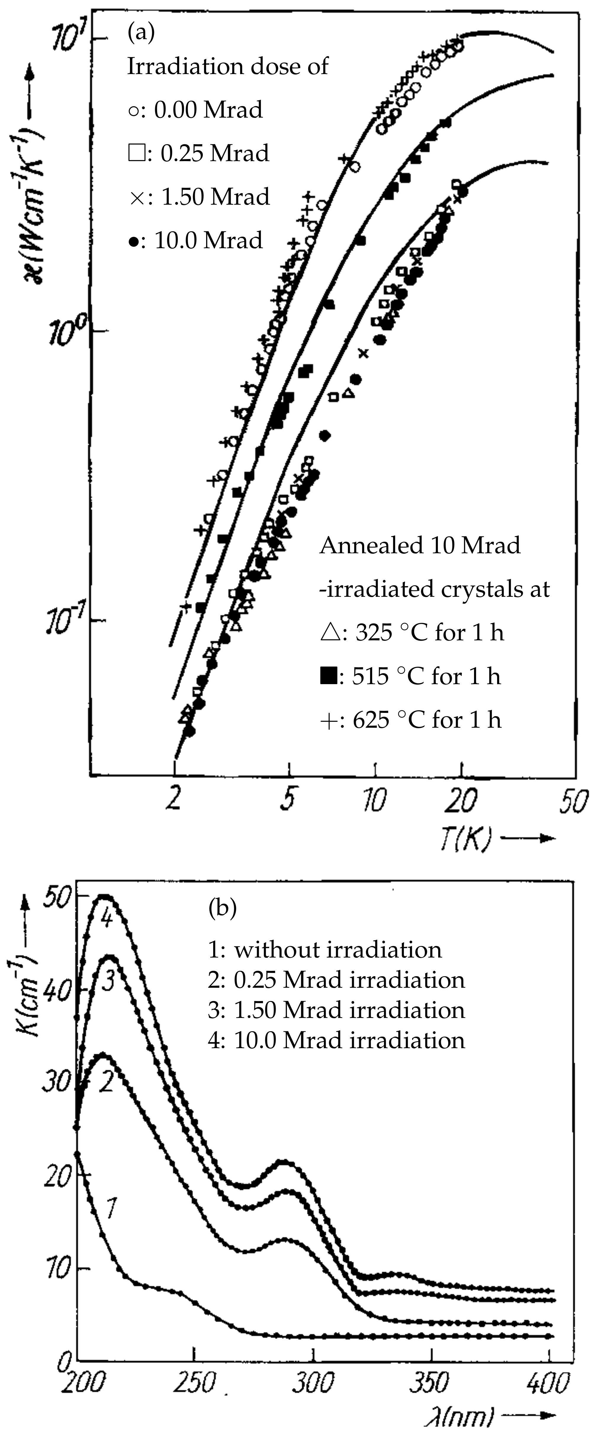
| MgO crystals | -ray, 2.1 MeV, up to 10 Mrad, , RT | thermal conductivity decreased by half; absorption increased by five times; fully recovered after annealing at for 1 h | [163] |
| MgO crystals | -ray, , , 0.8 Gy/s, | TSL intensity increased linearly with dose | [160] |
| MgO crystals | -ray, , , , | TSL intensity was very weakly dependent on dose | [160] |
| MgO powder | -ray (Co), , ∼, stored at RT for 1 year before measurement | TL changed after irradiation | [164] |
| MgO powder | -ray (Co), , – | TL changed with dose | [165] |
| Ag/MgO/Ag | -ray, 0.662 MeV, up to 32.55 mGy | capacitance increased with dose | [121] |
| CoFeB films | -ray, 1.2 MeV, , | sensitive to -ray irradiation | [118] |
| MgO/CoFeB | -ray, 100 kRad | no noticeable change in magnetic properties | [166] |
| CoFeB/MgO/CoFeB | Co, -ray, 1 Mrad | no effect | [119] |
| CoFeB/MgO/CoFeB | Co, -ray, 10 Mrad, 9.78 rad/min | highly tolerant of -ray radiation | [152] |
| CoFeB/MgO/CoFeB | Co, -ray, below 20 Mrad, , RT | coercivity increased with irradiation while saturation magnetization was not affected | [120] |
Disclaimer/Publisher’s Note: The statements, opinions and data contained in all publications are solely those of the individual author(s) and contributor(s) and not of MDPI and/or the editor(s). MDPI and/or the editor(s) disclaim responsibility for any injury to people or property resulting from any ideas, methods, instructions or products referred to in the content. |
© 2023 by the authors. Licensee MDPI, Basel, Switzerland. This article is an open access article distributed under the terms and conditions of the Creative Commons Attribution (CC BY) license (https://creativecommons.org/licenses/by/4.0/).
Share and Cite
Seifu, D.; Peng, Q.; Sze, K.; Hou, J.; Gao, F.; Lan, Y. Electromagnetic Radiation Effects on MgO-Based Magnetic Tunnel Junctions: A Review. Molecules 2023, 28, 4151. https://doi.org/10.3390/molecules28104151
Seifu D, Peng Q, Sze K, Hou J, Gao F, Lan Y. Electromagnetic Radiation Effects on MgO-Based Magnetic Tunnel Junctions: A Review. Molecules. 2023; 28(10):4151. https://doi.org/10.3390/molecules28104151
Chicago/Turabian StyleSeifu, Dereje, Qing Peng, Kit Sze, Jie Hou, Fei Gao, and Yucheng Lan. 2023. "Electromagnetic Radiation Effects on MgO-Based Magnetic Tunnel Junctions: A Review" Molecules 28, no. 10: 4151. https://doi.org/10.3390/molecules28104151
APA StyleSeifu, D., Peng, Q., Sze, K., Hou, J., Gao, F., & Lan, Y. (2023). Electromagnetic Radiation Effects on MgO-Based Magnetic Tunnel Junctions: A Review. Molecules, 28(10), 4151. https://doi.org/10.3390/molecules28104151