Article

A Novel Two-Dimensional ZnSiP2 Monolayer as an Anode Material for K-Ion Batteries and NO2 Gas Sensing

1
Henan International Joint Laboratory of MXene Materials Microstructure, College of Physics and Electronic Engineering, Nanyang Normal University, Nanyang 473061, China
2
College of mechanical and electrical engineering, Nanyang Normal University, Nanyang 473061, China
3
College of Material Science and Engineering, Guilin University of Technology, Guilin 541004, China
*
Authors to whom correspondence should be addressed.
Molecules 2022, 27(19), 6726; https://doi.org/10.3390/molecules27196726
Submission received: 15 September 2022 / Revised: 4 October 2022 / Accepted: 5 October 2022 / Published: 9 October 2022
(This article belongs to the Special Issue Computational Chemistry for Material Research)

Abstract

:
Using the crystal-structure search technique and first-principles calculation, we report a new two-dimensional semiconductor, ZnSiP2, which was found to be stable by phonon, molecular-dynamic, and elastic-moduli simulations. ZnSiP2 has an indirect band gap of 1.79 eV and exhibits an anisotropic character mechanically. Here, we investigated the ZnSiP2 monolayer as an anode material for K-ion batteries and gas sensing for the adsorption of CO, CO2, SO2, NO, NO2, and NH3 gas molecules. Our calculations show that the ZnSiP2 monolayer possesses a theoretical capacity of 517 mAh/g for K ions and an ultralow diffusion barrier of 0.12 eV. Importantly, the ZnSiP2 monolayer exhibits metallic behavior after the adsorption of the K-atom layer, which provides better conductivity in a period of the battery cycle. In addition, the results show that the ZnSiP2 monolayer is highly sensitive and selective to NO2 gas molecules.

1. Introduction

Two-dimensional semiconductor (2D) materials have potential applications in electronic equipment, catalysis, electrode materials, and gas sensors owing to their significant electrical, physical, and chemical properties [1,2,3,4]. In particular, the large surface areas, excellent mechanical strengths, and strong surface activities of 2D materials provide excellent advantages for the adsorption of certain metal atoms and gas molecules, which make 2D materials suitable as anodes for metal-ion batteries and gas sensors [5,6]. Recently, many novel 2D semiconductors [7,8,9,10,11,12,13,14,15,16,17,18] have attracted much attention due to their high stabilities, good electronic properties, high capacities for metal-ion batteries, and high sensitivities toward certain gases, such as NO2, SO2, and NH3.
As a new family of 2D materials, phosphorus carbides (PCs) with α phase and β phase are semiconductors that exhibit highly anisotropic electronic characters with high carrier mobilities. More importantly, α-PC and β-PC, as promising anode materials for Li-, Na-, and K-ion batteries, having high capacities and fast diffusion channels for Li, Na, and K ions [10,11]. It has also been predicted that α-PC, as a promising gas sensor, exhibits superior selectivity and sensitivity for NO2 [12]. Buckled-graphene-like PC6, as a semiconductor, has been predicted to have ultrahigh carrier mobility and, as an anode for Li-ion batteries, a high capacity of 717 mAh/g and an open-circuit voltage of 0.21 V [13]. Furthermore, typical 2D metal-phosphide δ-InP3 exhibits high electron mobility and has been shown to be usable as a N-based gas sensor with high selectivity and sensitivity and good reversibility [16]. In addition, metal oxides, such as two-dimensional WO3 and Pd-loaded ZnO monolayers, are important semiconductors applied in gas sensors, with high sensitivities [19,20].
Apart from the excellent performances of binary semiconductors, ternary 2D semiconductor materials have also attracted special interest. Using the epitaxial growth technique, Beniwal and co-workers [21] synthesized a 2D hexagonal graphenic BCN monolayer, which showed semiconductor behavior with a band gap of 1.50 eV, high directional anisotropy, a small Young’s modulus, high flexibility, and suitability as a potential electrode material for Al-based dual-ion batteries [22]. Recently, a new semiconductor BCN structure, by the global-optimization search method, was predicted to have high carrier mobility and excellent optical properties [23]. Using first-principles simulations, two-dimensional BC2P and BC3P3 monolayers were also predicted to present semiconductors with proper band gaps and low barriers for the dissociation of water and hydrogen molecules and thus to show promise for use in renewable energy [24]. Recently, Tang et al. [25] designed a BC6P monolayer isostructural and isoelectronic to graphene that has high electron mobility and can be used in K-ion batteries, with a high capacity of 1410 mAh/g.
In recent years, we have noticed that the bulk ternary chalcopyrite-structure compound ZnSiP2 is a promising semiconductor that has been synthesized experimentally [26,27] and used for optical, optoelectronic, photovoltaic, and thermoelectric applications [28,29,30,31]. However, its 2D structure is still unclear and has not been studied. In this paper, we predicted a stable structure of the 2D semiconductor ZnSiP2 and studied its electronic, mechanical properties as well as its electrode performance for K-ion batteries (KIBs). ZnSiP2, as an electrode for K-ion batteries, has a high theoretical storage capacity of 517 mAh/g and a low diffusion energy of 0.12 eV. In addition, its gas-sensing performance was investigated by simulation of the adsorption of CO, CO2, SO2, NO, NO2, and NH3 gas molecules on the ZnSiP2 monolayer. Our calculation results demonstrate that the strong adsorption ability with respect to K ions and NO2 gas molecules on the ZnSiP2 monolayer makes it a promising anode for K-ion batteries and gas sensors for NO2.

2. Results and Discussion

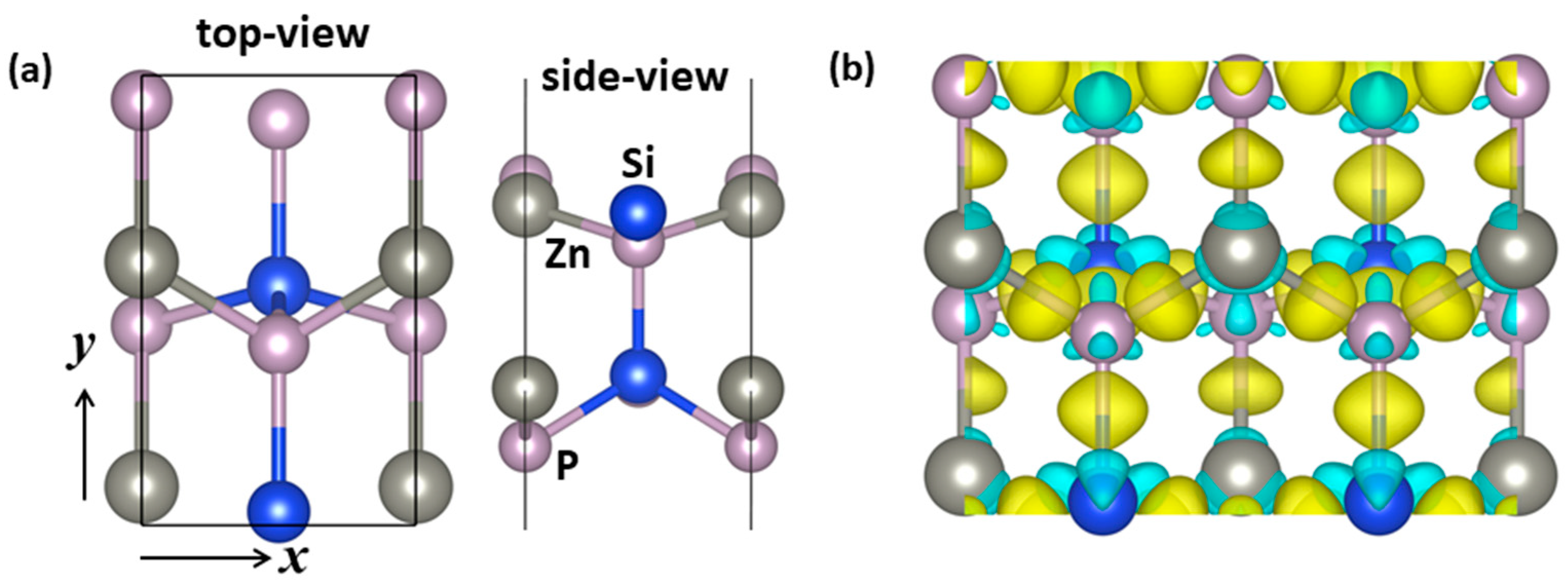
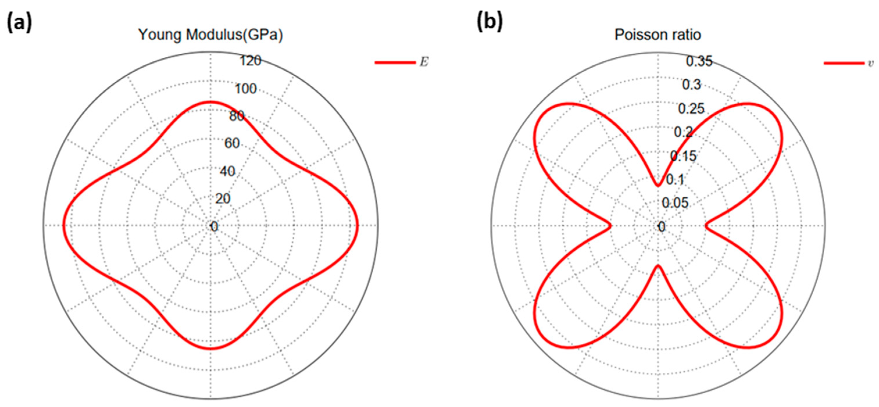
2.1. Structure and Stability

By using the global-structure search method, we found a new ZnSiP2 monolayer with the space group Pmc21 (no. 26) containing two formula units. The structure crystalized in an orthorhombic structure, and the optimized lattice parameters were a = 3.7251 and b = 6.1398 Å. As shown in Figure 1a, a remarkable feature is that the ZnSiP2 monolayer is stacked as a bilayer hexagonal lattice, and the two layers are bonded by Si and P, with a distance of 2.286 Å. Each layer was arranged alternately in two kinds of hexagonal rings. One ring was composed of one Si, two Zn, and three P atoms; the other ring was composed of one Zn, two Si, and three P atoms, which gave rise to two types of bonds: Si-P and Zn-P. To understand the chemical-bonding nature, the charge density difference was calculated and shown in Figure 1b, which is defined as the difference between the total electron density of the ZnSiP2 monolayer and the charge density of isolated Zn, Si, and P atoms at their specified positions. It can clearly be seen that there is a strong non-polar covalent bond between Si and P [32]. Regarding the Zn-P bonds, the polar covalent bonds between Zn and P atoms were due to the transfer charges shifted toward P atoms.
The cohesive energy is a key factor in experimental synthesis, which is calculated by E coh = ( 2 E Si + 2 E Zn + 4 E P E ZnSiP 2 ) / 8 , where E Si , E Zn , E P , and E ZnSiP 2 represent the energies of one Si, Zn, P, and perfect ZnSiP2, respectively. The calculated cohesive energy of the ZnSiP2 monolayer was 4.36 eV/atom, which is comparable to those of phophorene (3.30 eV/atom) [33], germanene (3.26 eV/atom), silicene (3.98 eV/atom) [34], and SiP (4.16 eV/atom) [35]. We further calculated the formation energy of the ZnSiP2 monolayer related to the SiP2 monolayer and Zn metal to investigate its stability, which was calculated by E f = E ZnSiP 2 μ SiP 2 m μ Zn ( bulk ) , where μ SiP 2 , μ Zn ( bulk ) , and E ZnSiP 2 are the energies of two-dimensional SiP2 [36], one Zn atom in bulk Zn metal, and the perfect ZnSiP2 monolayer, respectively, and m is the number of Zn atoms. The calculated formation energy is −0.465 eV, the negative value further indicating that the ZnSiP2 monolayer may be synthesized. The phonon spectrum was used to check the dynamic stability of the ZnSiP2 monolayer. The calculated phonon dispersion curves for the ZnSiP2 monolayer are shown in Figure 2a; all frequencies in the Brillouin region were positive, which means that the ZnSiP2 monolayer is dynamically stable. Furthermore, thermal stability was checked by AIMD simulation running for 10 ps at 400 K (Figure 2b); the structure remained almost intact at the end of the simulation, revealing that the ZnSiP2 monolayer has good thermal stability. According to the above analysis, the predicted 2D ZnSiP2 is promising for experimental synthesis.
Additionally, we further calculated the four independent elastic constants of the ZnSiP2 monolayer, which were C 11 = 106.2 Nm−1, C 22 = 86.0 Nm−1, C 12 = 8.6 Nm−1, and C 44 = 26.1 Nm−1. According to the obtained elastic constants, the ZnSiP2 monolayer satisfied the mechanical stability standard: C 11 > 0 ; C 44 > 0 ; C 11 C 22 > C 12 2 [37]. Moreover, the diagrams for the in-plane Young’s modulus and Poisson ratio with polar angle [38] could be obtained and are depicted in Figure 3, showing that the ZnSiP2 monolayer is anisotropic. The maximum Young’s modulus (105 N/m) was higher than that reported for phosphorene (92 N/m) [39] and comparable to those of MoS2 (129 N/m) [40] and V2Te2O monolayers (115.3 N/m) [41]. The anisotropy characteristic of mechanical properties also has an important effect on electronic properties.

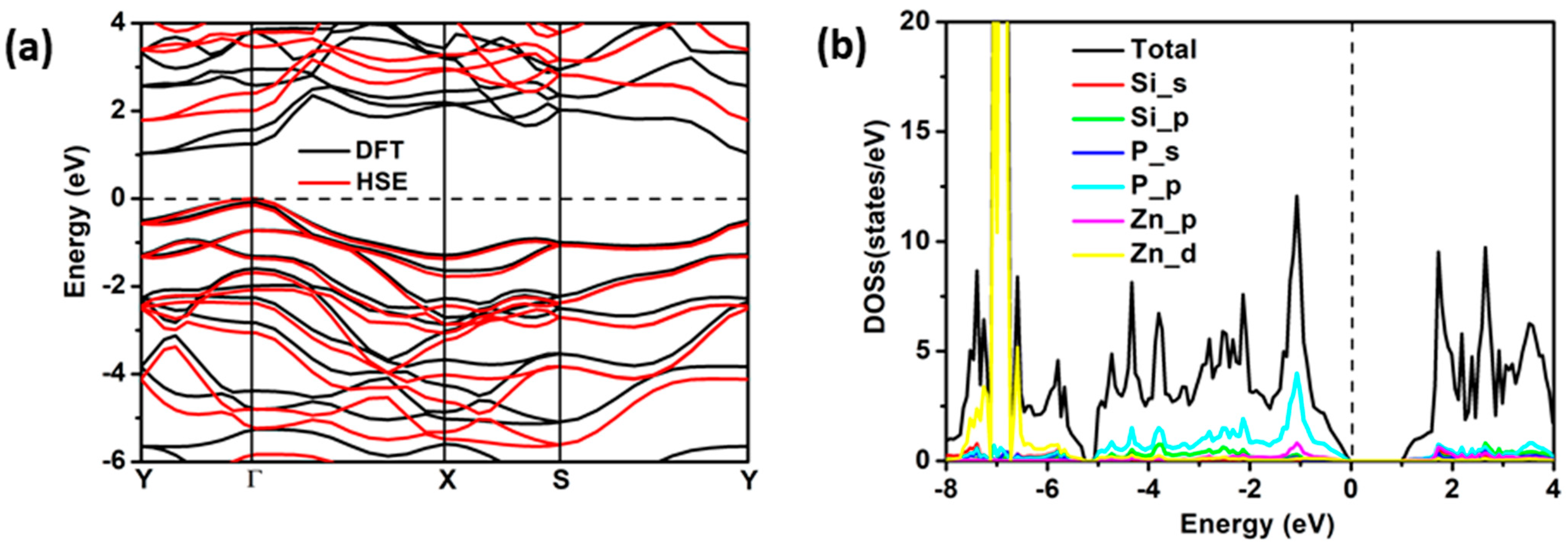
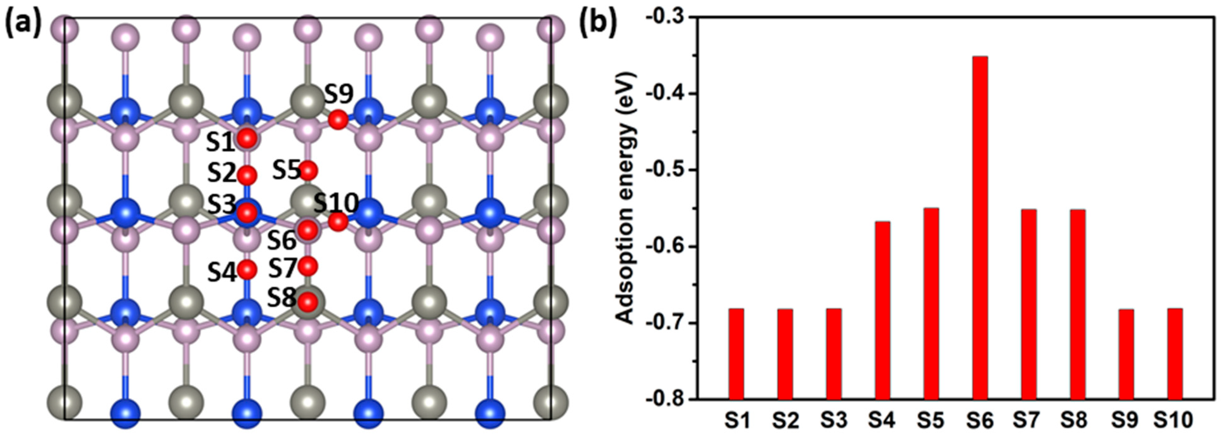
2.2. Electronic and Adsorption Properties

The calculated band structure and density of states for the ZnSiP2 monolayer are shown in Figure 4a,b. The valence band maximum (VBM) is at point Γ, and the conduction band minimum (CBM) is at point Y. Therefore, as an indirect semiconductor, the band-gap values derived from the PBE and HSE calculations were 1.04 and 1.79 eV, respectively. The band dispersion near the VBM and CBM shows an anisotropic character, which results in the anisotropy of the effective masses. According to the formula m * = 2 E 2 / k 2 , the obtained electron effective masses near the CBM were 1.364 m0 and 0.333 m0 along the x-and y-directions, while the hole effective masses near the VBM were 1.019 m0 and 0.433 m0 along the x- and y-directions, respectively. The density of states in Figure 4b shows that the VBM and CBM are both mainly contributed to by P 2p and Zn 4d orbitals.
To further study the performance of the ZnSiP2 monolayer as an electrode material, we investigated the adsorption properties of one K atom on its surface using a 3 × 2 × 1 supercell as the substrate. According to the structural symmetry, ten possible K-atom adsorption sites (S1–S10) with adsorption energies based on Equation (1) were considered and calculated, as shown in Figure 5. After geometric-structure optimization, we found some equivalent sites due to the transfer of K atoms from one site to another site. As can be clearly seen in Figure 5b, the equivalent sites were S1 = S2 = S3 = S9 = S10 and S5 = S7 = S8, so only four sites S2, S4, S5, and S6 were left, with adsorption energies of −0.68, −0.57, −0.55, and −0.35 eV, respectively. Thus, the adsorption energy of the K atom at S2 site was the lowest, which means that the adsorbed K atoms prefer to stay at the bridge position of Si-P to reduce the Coulomb repulsion between K and Zn. The nearest K-P, K-Zn and K-Si distances are 3.30 Å, 3.92 Å and 3.53 Å, respectively.
To assess the adsorption behavior of the K atoms, we calculated the charge-density differences shown in Figure 6a, which is defined by:
Δ ρ = ρ ( K Z n 12 S i 12 P 24 ) - ρ ( K ) - ρ ( Z n 12 S i 12 P 24 )  
where ρ ( Z n 12 S i 12 P 24 ) , ρ ( K Z n 12 S i 12 P 24 ) , and ρ ( K ) are the charge densities of the Zn12Si12P24 monolayer with adsorbed K atoms, the substrate Zn12Si12P24, and an isolated K atom, respectively. Obvious charge transfer could be observed, and the K atoms had a net charge of 0.84 | e | based on the Bader charge analysis, which implies charge transfer from the K atoms to the adjacent P and Si atoms in the Z n 12 S i 12 P 24 surface.
The diffusion barrier of K ions is a key parameter in estimating the performance of a battery. Next, the diffusion of one K ion on the ZnSiP2 surface was investigated. The possible diffusion path (inset of Figure 6b) between the lowest-energy adsorption sites and the calculated results is shown in Figure 6b. The diffusion barrier of the path was 0.12 eV, which is comparable to the result for ReN2 (0.127 eV) [42]. Compared with other anode materials, ZnSiP2 has a low K-ion diffusion barrier that is smaller than those of BP (0.155 eV) [43], PC6 (0.26 eV) [44], and SnC (0.17 eV) [45]. However, this value is larger than those of GeS (0.05 eV) [46], Ti3C2 (0.103 eV) [47], and C6BN (0.087 eV) [48]. The low diffusion barrier can result in ultrafast charging–discharging cycles in K-ion batteries.

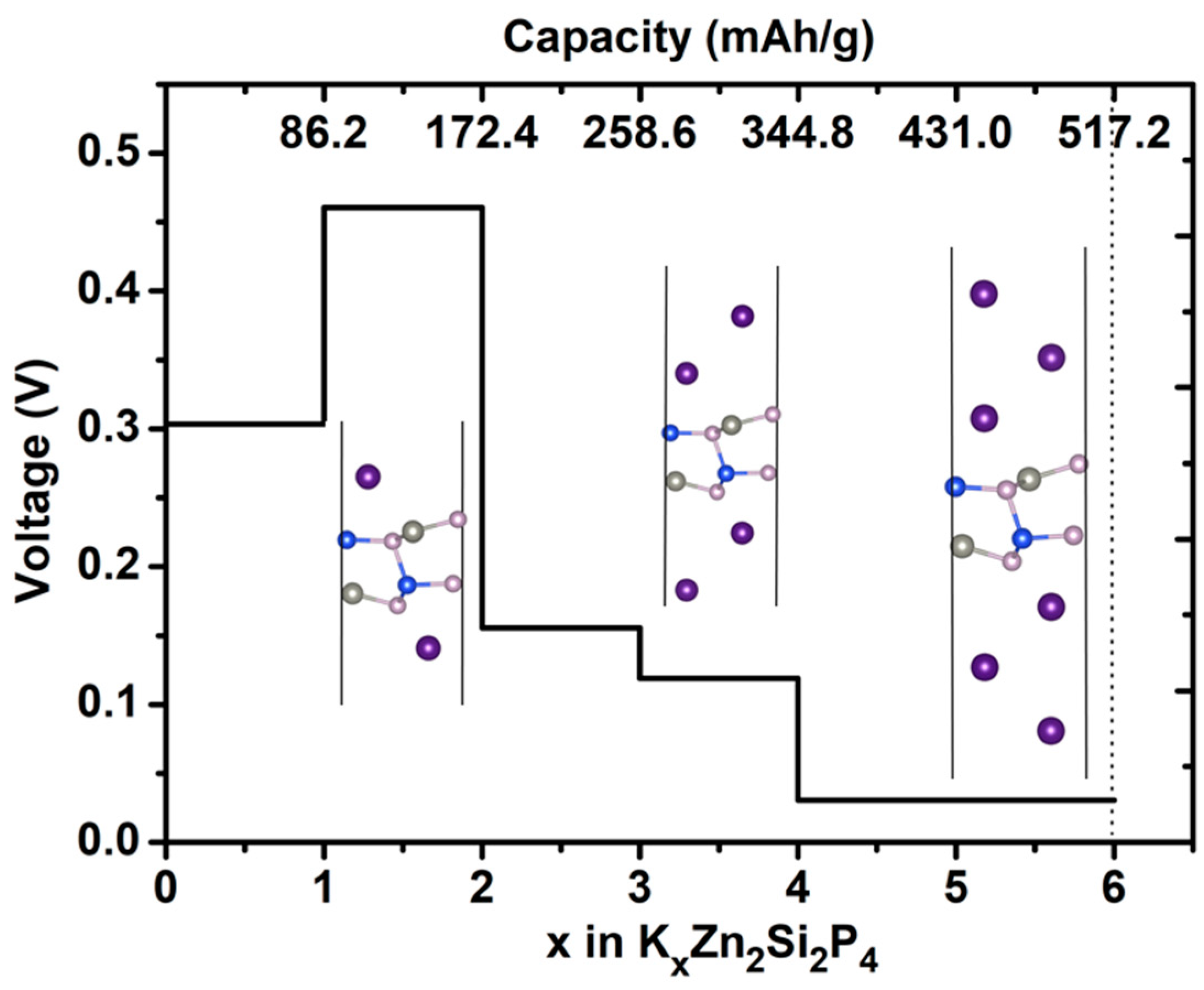
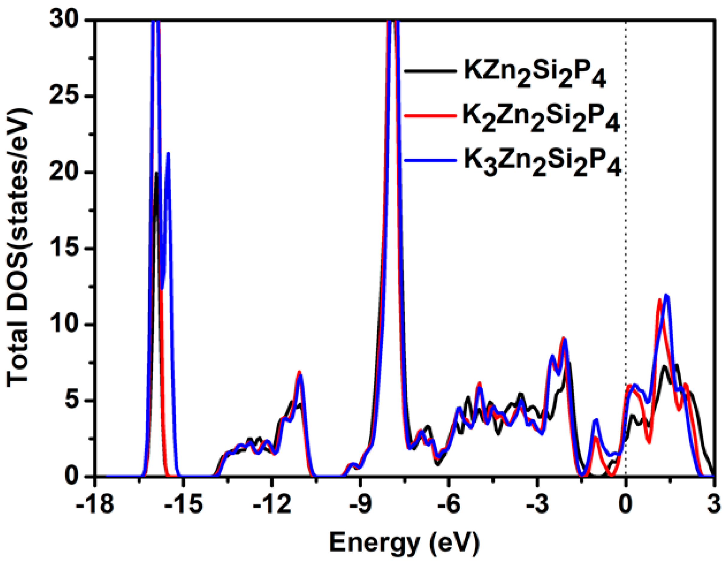
2.3. Capacity and Open-Circuit Voltage

After studying the adsorption and diffusion behavior of one K atom on the supercell of the ZnSiP2 monolayer, we then explored the behavior of K adsorption concentration. Five K concentrations (KxZn2Si2P4, x = 1–4, 6) were considered, and the average adsorption energies acquired according to Equation (2) were −0.30, −0.46, −0.16, −0.12, and −0.03 eV, respectively. It is to be noted that the K concentration reached x = 6, still showing negative adsorption energy, which means that K atoms can be adsorbed on the ZnSiP2 monolayer. The three stable adsorption configurations (K2Zn2Si2P4, K4Zn2Si2P4, and K6Zn2Si2P4) are shown in the inset of Figure 7. The first and the second K atom layers are located at S2 and S5 sites, with both sides of the ZnSiP2 monolayer. As for the third K-atom layer, the K atom prefers to stay at the S2 site. The stoichiometry K6Zn2Si2P4 can provide the maximal storage capacity 517 mAh/g, according to Equation (4), which is higher than other reported values for 2D materials, such as GeS (256 mAh/g) [46], ReN2 (250 mAh/g) [42], Ti3C2 (191 mAh/g) [47], MoS2/Ti2CS2 (141 mAh/g) [49], and MoN2 (432 mAh/g) [50], but lower than the capacities for BC3 (858 mAh/g) [51], BC6P (1410 mAh/g) [25], C6BN (533 mAh/g) [48], BP (570 mAh/g) [43], and V2S2O (883.6Ah/g) [41]. Based on Equation (3), OCVs were obtained and are shown in Figure 7, and the calculated values for different concentrations, KZn2Si2P4, K2Zn2Si2P4, K3Zn2Si2P4, K4Zn2Si2P4, and K6Zn2Si2P4, were 0.30, 0.46, 0.16, 0.12, and 0.03 V, respectively. The Bader analysis showed that every K atom transfers 0.58 e to ZnSiP2 when two K atoms are absorbed on the surface of 2D ZnSiP2, while every K atom transfers 0.51 e to ZnSiP2 when only one K atom is absorbed on the surface of 2D ZnSiP2, implying that two K atoms are more easily absorbed on the surface of 2D ZnSiP2 than one K atom. So, the OCV increases as x increases from 1 to 2, as shown in Figure 7. However, the overall voltage decreases as the capacity increases.
Importantly, the density states of the three stable adsorption configurations (KZn2Si2P4, K2Zn2Si2P4, and K3Zn2Si2P4) were calculated using the PBE functional, and ZnSiP2, after the adsorption of K atoms, showed metallic behavior, as shown in Figure 8, which is beneficial for the ZnSiP2 monolayer as an electrode material.

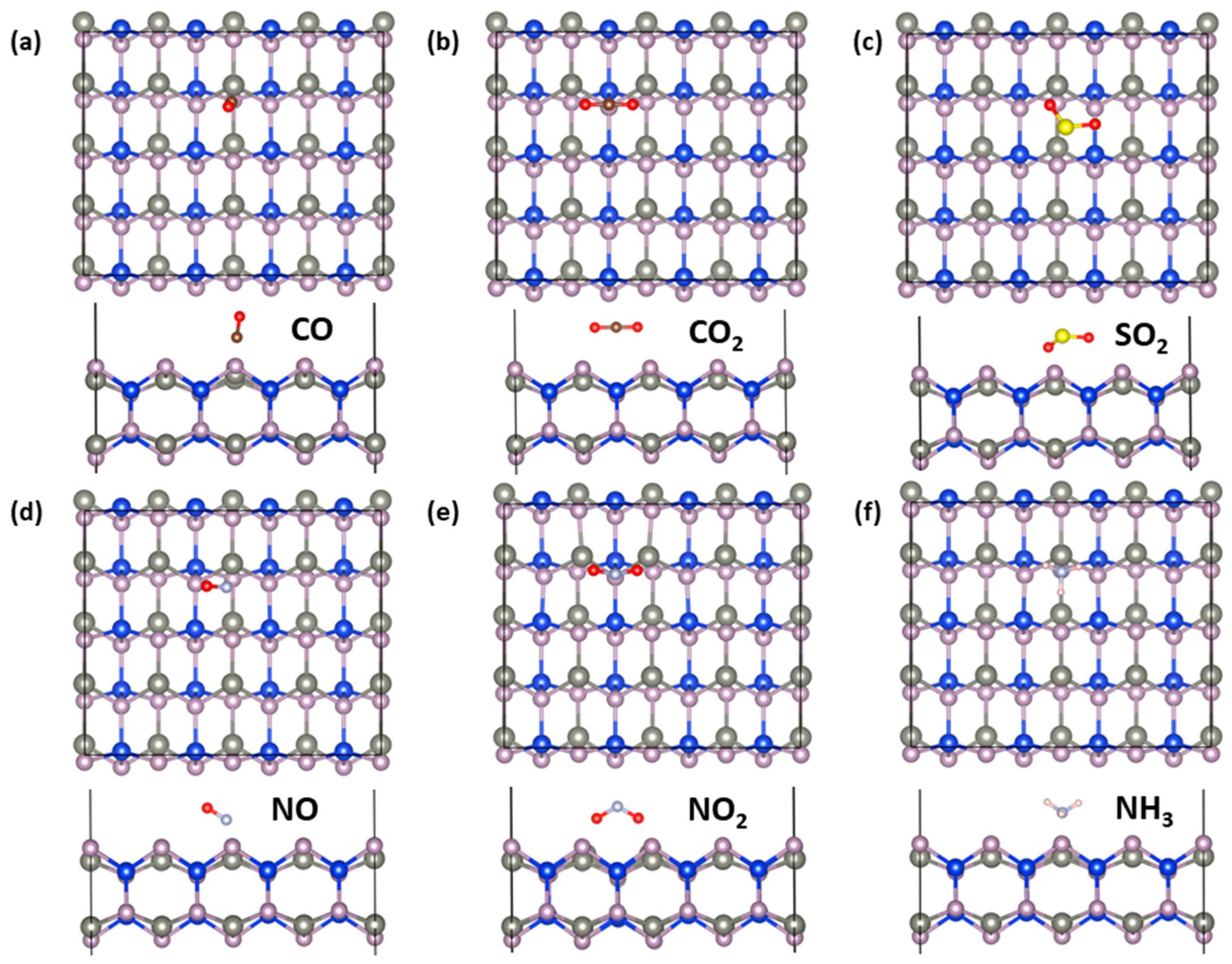
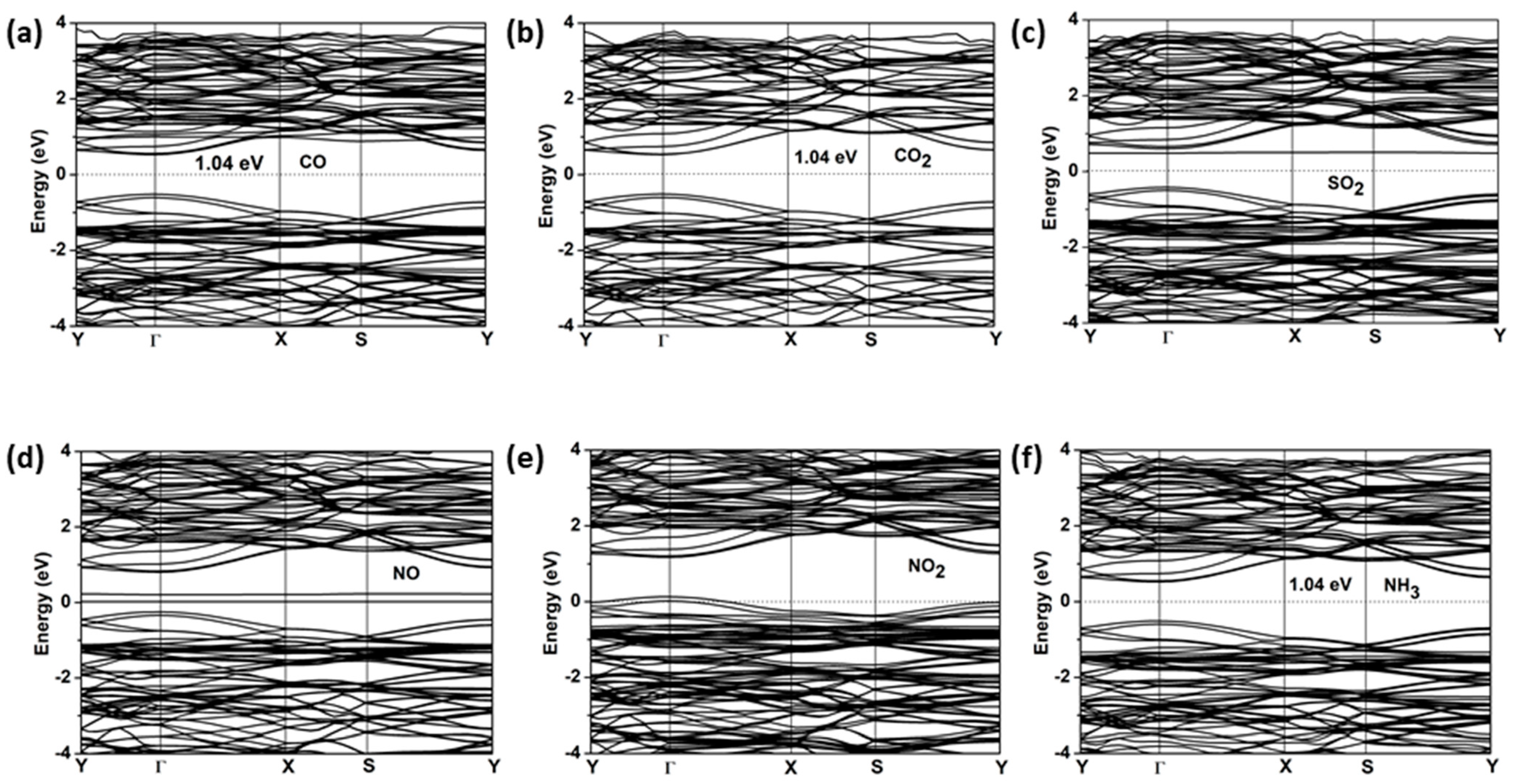
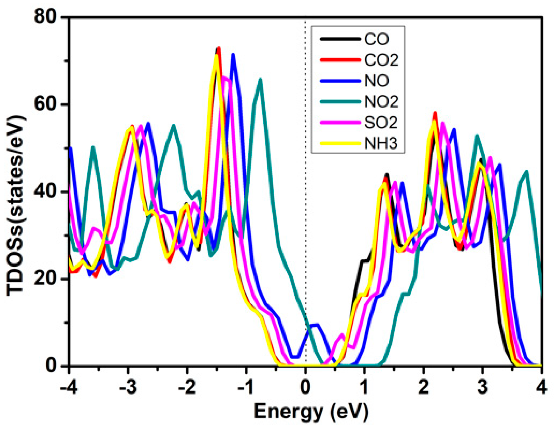
2.4. Gas-Sensing Properties

To further study the gas-sensing ability of the ZnSiP2 monolayer, we systematically studied the adsorption behavior of gas molecules (CO, CO2, SO2, NO, NO2, and NH3) on its surface by first-principles simulations. The most stable configurations of the gas molecules adsorbed on the ZnSiP2 monolayer are shown in Figure 9, and the corresponding adsorption energies (Ead), adsorption distances (d0), band gaps after molecule adsorption (Eg), and charge transfers (Q) are listed in Table 1. A positive charge for Q means charge transfer from the monolayer to the gas molecules. The equilibrium distance of 1.53 Å between NO2 and the monolayer revealed that NO2 forms a stable chemical bond. Moreover, the NO2 molecules showed high adsorption energies, indicating that ZnSiP2 is more sensitive to NO2 molecules than the other five molecules. As shown in Table 1, the Bader charge analysis indicated that there were 0.24, 0.12, 0.67, and 0.13 electron transfers between the molecules and the substrates for SO2, NO, NO2, and NH3, which further implies that NO2 molecules have strong chemical interactions with the ZnSiP2 monolayer.
The electronic band structures and densities of states for gas-ZnSiP2 are shown in Figure 10 and Figure 11, respectively. All the systems, except for NO and NO2, that adsorbed the ZnSiP2 monolayer became direct band-gap semiconductors, and both VBM and CBM were at the Gamma point. It can be clearly seen from Figure 10 and Figure 11 that the NO and NO2 adsorbed on the ZnSiP2 monolayer introduced a high density of states at the Fermi surface, which made the ZnSiP2 exhibit a metallic character and changed the electronic properties of the ZnSiP2 monolayer easily. The adsorption of CO, CO2, and NH3 had no significant effect on the band structure, and the band gaps did not change much. For SO2 adsorption (see Figure 10c), the shallow donor energy levels were introduced into the energy band, resulting in the narrowing of the band gap. Combining all the above results, we can conclude that the ZnSiP2 monolayer is promising as a sensor of NO2 gas molecules with high selectivity and sensitivity.

3. Computational Methods

To find the lowest energy structure of 2D ZnSiP2, a swarm-intelligence-based PSO method, implemented in CALYPSO code [52,53], combined with first-principles calculations, was employed, which has been used to successfully predict many 2D systems, such as Cu2Si, PC6, SnP3, and B2N3 [19,34,54,55]. The structures of 2D ZnSiP2 were searched with the simulation cells containing 1–4 formula units. The population size and the number of generations were both set to 30, which have been tested to give convergent results. In the first generation, a population of the structures was generated randomly. In the following generation, 60% of the population was generated from the lowest energy structures in the previous generation and all of the structures were fully relaxed, including the atomic positions and the lattice parameters.
The first-principles calculations based on density functional theory were performed using the projector-augmented wave (PAW) method, as implemented in VASP software [56,57,58]. The exchange correlation potential was described using Perdew–Burke–Ernzerhof (PBE) generalized gradient approximation [59] and corrected by the van der Waals (vdW) interaction in the calculation of the adsorption properties of ZnSiP2. The plane-wave energy cut-off and Monkhorst–Pack K-point mesh density were set to 500 eV and 2π × 0.03 Å−1, respectively. All geometries were optimized and relaxed until a total energy change smaller than 10−6 eV and a force tolerance acting on each atom less than 0.001 eVÅ−1 was achieved. In order to make the band-gap calculation more accurate for semiconductors, the HSE06 functional was employed [60]. A vacuum thickness of 25 Å was used to avoid the interlayer interactions. The nudged elastic band (NEB) method was used to obtain the K-ion diffusion energy barrier. To assess the dynamic stability, phonon spectra were calculated using the PHONOPY code [61]. In addition, ab initio molecular dynamics (AIMD) were explored with the NVT ensemble to examine the thermal stability.
In order to study the interactions between metals (gas molecules) and substrates, adsorption energies and adsorption distances were systematically calculated, according to the following equation:
E ad = ( E total n E metal ( gas ) E ZnSiP 2 ) n
where E total , E ZnSiP 2 , and E metal ( gas ) represent the total energy of the metal (gas molecules) adsorbed on the ZnSiP2 monolayer, the perfect ZnSiP2 monolayer, and the metal in the bulk metal or gas molecules, respectively, and n is the number of adsorbed metal atoms.
The adsorption stability of the K-ion layer on the ZnSiP2 monolayer is estimated by average adsorption energy, which is calculated using the following formula:
E av = E n total E ( n 1 ) total m E K m
where E n total and E ( n 1 ) total refer to the total energies of the ZnSiP2 monolayer with n and (n−1) layers and m is the number of K atoms in every layer.
For a given concentration x of KxZn2Si2P4, the open-circuit voltage (OCV) can be obtained with the following equation:
V = E ( x 2 ) E ( x 1 ) ( x 2 x 1 ) E K e ( x 2 x 1 )
where E ( x 2 ) and E ( x 1 ) are the total energies of KxZn2Si2P4 at two adjacent K-ion concentrations x 2 and x 1 , e is the element charge, and E K is the energy of one K atom in the bulk K metal.
The theoretical capacity can be evaluated from:
C M = c F M
where c is the number of adsorbed K atoms per ZnSiP2 unit, F is the Faraday constant (26,801 mAhmol−1), and M is the molar weight of ZnSiP2 in gmol−1.

4. Conclusions

In summary, we predicted the ZnSiP2 monolayer as a new 2D semiconductor material which can be used as an anode material for K-ion batteries and NO2 gas sensors by the global-optimization algorithm combined with first-principles calculation. Phonon simulation, molecular dynamics, and elastic-constant calculations confirmed its stability. The calculated electronic structure and mechanical properties indicate that ZnSiP2 has an indirect band gap of 1.79 eV and exhibits anisotropic mechanical characteristics. Furthermore, we investigated 2D ZnSiP2 as an anode for KIBs. The ZnSiP2 monolayer has a theoretical capacity of 517 mAh/g for K-ions and a low diffusion barrier of 0.12 eV. In addition, we also investigated the gas-sensing properties of the ZnSiP2 monolayer with six gas molecules (CO, CO2, SO2, NO, NO2, and NH3). The results show that the ZnSiP2 monolayer is a promising gas sensor for NO2 with high sensitivity and selectivity.

Author Contributions

Conceptualization, C.P. and D.Z.; formal analysis, C.P., Z.W. and X.T.; writing—original draft preparation, C.P.; writing—review and editing, D.Z. and J.C.; funding acquisition, D.Z., C.P. and J.C. All authors have read and agreed to the published version of the manuscript.

Funding

This research was funded by Henan Joint Funds of the National Natural Science Foundation of China (grant no. U1904612), the Natural Science Foundation of Henan Province (grant nos. 222300420506, 222300420255).

Institutional Review Board Statement

Not applicable.

Informed Consent Statement

Not applicable.

Data Availability Statement

Data available on request from the authors.

Conflicts of Interest

The authors declare no conflict of interest.

Sample Availability

Samples of the compounds are available on request from the authors.

References

  1. Wang, Q.; Kalantar-Zadeh, K.; Kis, A.; Coleman, J.N.; Strano, M.S. Electronics and optoelectronics of two-dimensional transition metal dichalcogenides. Nat. Nanotechnol. 2012, 7, 699–712. [Google Scholar] [CrossRef]
  2. Jana, S.; Thomas, S.; Chi, H.L.; Jun, B.; Sang, U.L. Rational design of a PC3 monolayer: A high-capacity, rapidly charging anode material for sodium-ion batteries. Carbon 2020, 157, 420–426. [Google Scholar] [CrossRef]
  3. Mayorga-Martinez, C.C.; Sofer, Z.; Pumera, M. Layered black phosphorus as a selective vapor sensor. Angew. Chem. 2015, 54, 14317–14320. [Google Scholar] [CrossRef]
  4. Kumar, R.; Goel, N.; Kumar, M. UV-Activated MoS2 based fast and reversible NO2 sensor at room temperature. ACS Sens. 2017, 2, 1744–1752. [Google Scholar] [CrossRef]
  5. Lin, J.; Yu, T.; Han, F.; Yang, G. Computational predictions of two-dimensional anode materials of metal-ion batteries. Wiley Interdiscip. Rev. Comput. Mol. Sci. 2020, 10, 1473. [Google Scholar] [CrossRef] [Green Version]
  6. Kumar, V.; Azhikodan, D.; Roy, D.R. 2D Sb2C3 monolayer: A promising material for recyclable gas sensor for environmentally toxic nitrogen-containing gases (NCGs). J. Hazard. Mater. 2021, 405, 124168. [Google Scholar] [CrossRef]
  7. Wang, G.; Pandey, R.; Karna, S.P. Carbon phosphide monolayers with superior carrier mobility. Nanoscale 2016, 8, 8819–8825. [Google Scholar] [CrossRef] [Green Version]
  8. Guan, J.; Liu, D.; Zhu, Z.; Tomanek, D. Two-Dimensional phosphorus carbide: Competition between sp2 and sp3 bonding. Nano Lett. 2016, 16, 3247–3252. [Google Scholar] [CrossRef] [Green Version]
  9. Singh, D.; Kansara, S.; Gupta, S.K.; Sonvane, Y. Single layer of carbon phosphide as an efficient material for optoelectronic devices. J. Mater. Sci. 2018, 53, 8314–8327. [Google Scholar] [CrossRef]
  10. Li, F.; Liu, X.; Wang, J.; Zhang, X.; Yang, B.; Qu, Y.; Zhao, M. A promising alkali-metal ion battery anode material: 2D metallic phosphorus carbide (β0-PC). Electrochim. Acta 2017, 258, 582–590. [Google Scholar] [CrossRef]
  11. Qi, S.; Li, F.; Qu, Y.; Yang, Y.; Li, W.; Zhao, M. Prediction of a flexible anode material for Li/Na ion batteries: Phosphorous carbide monolayer (α-PC). Carbon 2019, 141, 444–450. [Google Scholar] [CrossRef]
  12. Wang, J.; Lei, J.; Yang, G.; Xue, J.; Cai, Q.; Chen, D.; Lu, H.; Zhang, R.; Zheng, Y. An Ultra-Sensitive and selective nitrogen dioxide sensor based on novel P2C2 monolayer from theoretical perspective. Nanoscale 2018, 10, 21936–21943. [Google Scholar] [CrossRef] [PubMed]
  13. Zhang, J.; Xu, L.; Yang, C.; Zhang, X.; Ma, L.; Zhang, M.; Lu, J. Two-dimensional single-layer PC6 as promising anode materials for Li-ion batteries: The first-principles calculations study. Appl. Surf. Sci. 2020, 510, 145493. [Google Scholar] [CrossRef]
  14. Lu, N.; Zhuo, Z.; Guo, H.; Wu, P.; Fa, W.; Wu, X.; Zeng, X.C. A new Two-dimensional functional material with desirable bandgap and ultrahigh carrier mobility. J. Phys. Chem. Lett. 2018, 9, 1728–1733. [Google Scholar] [CrossRef] [PubMed] [Green Version]
  15. Jing, Y.; Ma, Y.; Li, Y.; Heine, T. GeP3: A small indirect band gap 2D crystal with high carrier mobility and strong interlayer quantum confinement. Nano Lett. 2017, 17, 1833–1838. [Google Scholar] [CrossRef] [Green Version]
  16. Yi, W.; Chen, X.; Wang, Z.; Ding, Y.; Yang, B.; Liu, X. A novel two-dimensional δ-InP3 monolayer with high stability, tunable band gap, high carrier mobility, and gas sensing of NO2. J. Mater. Chem. C 2019, 7, 7352–7359. [Google Scholar] [CrossRef]
  17. Yu, T.; Zhao, Z.; Sun, Y.; Bergara, A.; Lin, J.; Zhang, S.; Xu, H.; Zhang, L.; Yang, G.; Liu, Y. Two-dimensional PC6 with direct band gap and anisotropic carrier mobility. J. Am. Chem. Soc. 2019, 141, 1599–1605. [Google Scholar] [CrossRef]
  18. Shen, Y.; Liu, J.; Li, X.; Wang, Q. Two-Dimensional T-NiSe2 as a promising anode material for Potassium-ion batteries with low average voltage, high ionic conductivity, and superior carrier mobility. ACS Appl. Mater. Interfaces 2019, 11, 35661–35666. [Google Scholar] [CrossRef]
  19. Li, J.; Wu, J.; Yu, Y. DFT exploration of sensor performances of two-dimensional WO3 to ten small gases in terms of work function and band gap changes and I-V responses. Appl. Surf. Sci. 2021, 546, 149104. [Google Scholar] [CrossRef]
  20. Chen, R.; Luo, S.; Xie, D.; Yu, Y.; Xiang, L. Highly dispersive palladium loading on ZnO by galvanic replacements with improved methane sensing performances. Chemosensors 2022, 10, 329. [Google Scholar] [CrossRef]
  21. Beniwal, S.; Hooper, J.; Miller, D.P.; Costa, P.S.; Chen, G.; Liu, S.Y.; Dowben, P.A.; Sykes, E.C.H.; Zurek, E.; Enders, A. Graphene-like boron-carbon-nitrogen monolayers. ACS Nano 2017, 11, 2486–2493. [Google Scholar] [CrossRef] [PubMed]
  22. Saini, H.; Das, S.; Pathak, B. BCN monolayer for high capacity Al-based dual-ion batteries. Mater. Adv. 2020, 1, 2418–2425. [Google Scholar] [CrossRef]
  23. Pu, C.; Li, C.; Lv, L.; Zhou, D.; Tang, X. Structure and optoelectronic properties for two dimensional BCN from first-principles calculations. Chin. J. Lumin. 2020, 41, 48–55. [Google Scholar] [CrossRef]
  24. Fu, X.; Guo, J.; Li, L.; Dai, T. Structural and electronic properties of predicting two-dimensional BC2P and BC3P3 monolayers by the global optimization method. Chem. Phys. Lett. 2019, 726, 69–76. [Google Scholar] [CrossRef]
  25. Tang, M.; Wang, C.; Schwingenschlogl, U.; Yang, G. BC6P Monolayer: Isostructural and isoelectronic analogues of graphene with desirable properties for K-Ion batteries. Chem. Mater. 2021, 33, 9262–9269. [Google Scholar] [CrossRef]
  26. Popov, V.P.; Pamplin, B.R. Epitaxial growth of solid solutions of ZnSiP2 in Si. J. Cryst. Growth 1972, 15, 129–132. [Google Scholar] [CrossRef]
  27. Martinez, A.D.; Miller, E.M.; Norman, A.G.; Schnepf, R.R.; Leick, N.; Perkins, C.; Stradins, P.; Toberer, E.S.; Tamdoli, A.C. Growth of amorphous and epitaxial ZnSiP2–Si alloys on Si. J. Mater. Chem. C 2018, 6, 2696–2703. [Google Scholar] [CrossRef]
  28. Martinez, A.D.; Warren, E.L.; Gorai, P.; Borup, K.A.; Kuciauskas, D.; Dippo, P.C.; Ortiz, B.R.; Macaluso, R.T.; Nguyen, S.D.; Greenaway, A.L.; et al. Solar energy conversion properties and defect physics of ZnSiP2. Energy Environ. Sci. 2016, 9, 1031–1041. [Google Scholar] [CrossRef] [Green Version]
  29. Scanlon, D.O.; Walsh, A. Bandgap engineering of ZnSnP2 for high-efficiency solar cells. Appl. Phys. Lett. 2012, 100, 251911. [Google Scholar] [CrossRef] [Green Version]
  30. Yuan, Y.; Zhu, X.; Zhou, Y.; Chen, X.; An, C.; Zhou, Y.; Zhang, R.; Gu, C.; Zhang, L.; Li, X.; et al. Pressure-engineered optical properties and emergent superconductivity in chalcopyrite semiconductor ZnSiP2. NPG Asia Mater. 2021, 13, 15. [Google Scholar] [CrossRef]
  31. Sreeparvathy, P.C.; Kanchana, V.; Vaitheeswaran, G. Thermoelectric properties of zinc based pnictide semiconductors. J. Appl. Phys. 2016, 119, 085701. [Google Scholar] [CrossRef] [Green Version]
  32. Liu, J.; Emrys, T.; Miao, J.; Huang, Y.; Rondinelli, J.M.; Hendrik, H. Understanding chemical bonding in alloys and the representation in atomistic simulations. J. Phys. Chem. C 2018, 122, 14996–15009. [Google Scholar] [CrossRef]
  33. Guan, J.; Zhu, Z.; Tománek, D. Phase coexistence and metal-insulator transition in few-layer phosphorene: A computational study. Phys. Rev. Lett. 2014, 113, 046804. [Google Scholar] [CrossRef] [PubMed] [Green Version]
  34. Yang, L.M.; Bačić, V.; Popov, I.A.; Boldyrev, A.I.; Heine, T.; Frauenheim, T.; Ganz, E. Two-dimensional Cu2Si monolayer with planar hexacoordinate copper and silicon bonding. J. Am. Chem. Soc. 2015, 137, 2757–2762. [Google Scholar] [CrossRef] [PubMed]
  35. Wu, J.; Li, J.; Yu, Y. A theoretical analysis on the oxidation and water dissociation resistance on group-IV phosphide monolayers. ChemPhysChem 2020, 21, 2539–2549. [Google Scholar] [CrossRef] [PubMed]
  36. Huang, B.; Zhuang, H.; Yoon, M.; Sumpter, B.G.; Wei, S. Highly stable two-dimensional silicon phosphides: Different stoichiometries and exotic electronic properties. Phys. Rev. B 2015, 91, 121401. [Google Scholar] [CrossRef] [Green Version]
  37. Mouhat, F.; Couder, F.X. Necessary and sufficient elastic stability conditions in various crystal systems. Phys. Rev. B 2014, 90, 224104. [Google Scholar] [CrossRef] [Green Version]
  38. Cadelano, E.; Palla, P.L.; Giordano, S.; Colombo, L. Elastic properties of hydrogenated grapheme. Phys. Rev. B 2010, 82, 235414. [Google Scholar] [CrossRef] [Green Version]
  39. Wang, L.; Kutana, A.; Zou, X.; Yakobson, B.I. Electro-mechanical anisotropy of phosphorene. Nanoscale 2015, 7, 9746–9751. [Google Scholar] [CrossRef]
  40. Cooper, R.C.; Lee, C.; Marianetti, C.A.; Wei, X.; Hone, J.; Kysar, J.W. Nonlinear elastic behavior of two-dimensional molybdenum disulfide. Phys. Rev. B 2013, 87, 035423. [Google Scholar] [CrossRef]
  41. Yu, Y. High storage capacity and small volume change of potassium-intercalation into novel vanadium oxychalcogenide monolayers V2S2O, V2Se2O and V2Te2O: An ab initio DFT investigation. Appl. Surf. Sci. 2021, 546, 149062. [Google Scholar] [CrossRef]
  42. Zhang, S.H.; Liu, B.G. Superior ionic and electronic properties of ReN2 monolayers for Na-ion battery electrodes. Nanotechnology 2018, 29, 325401. [Google Scholar] [CrossRef] [PubMed] [Green Version]
  43. Jiang, H.; Shyy, W.; Liu, M.; Wei, L.; Wu, M.; Zhao, T.S. Boron phosphide monolayer as a potential anode material for alkali metal-based batteries. J. Mater. Chem. A 2017, 5, 672–679. [Google Scholar] [CrossRef]
  44. Dou, K.; Ma, Y.; Zhang, T.; Huang, B.; Dai, Y. Prediction of two-dimensional PC6 as a promising anode material for potassium-ion batteries. Phys. Chem. Chem. Phys. 2019, 21, 26212–26218. [Google Scholar] [CrossRef]
  45. Rehman, J.; Fan, X.; Laref, A.; Zheng, W.T. Adsorption and diffusion of potassium on 2D SnC sheets for potential high-performance anodic applications of potassium-ion batteries. ChemElectroChem 2020, 7, 3832–3838. [Google Scholar] [CrossRef]
  46. Li, F.; Qu, Y.; Zhao, M. Germanium sulfide nanosheet: A universal anode material for alkali metal ion batteries. J. Mater. Chem. A 2016, 4, 8905–8912. [Google Scholar] [CrossRef]
  47. Er, D.; Li, J.; Naguib, M.; Gogotsi, Y.; Shenoy, V. Ti3C2 MXene as a high capacity electrode material for metal (Li, Na, K, Ca) ion batteries. ACS Appl. Mater. Interfaces 2014, 6, 11173–11179. [Google Scholar] [CrossRef]
  48. Xiang, P.; Sharma, S.; Wang, Z.M.; Wu, J.; Schwingenschlogl, U. Flexible C6BN monolayers as promising anode materials for high-performance K-ion batteries. ACS Appl. Mater. Interfaces 2020, 12, 30731–30739. [Google Scholar] [CrossRef]
  49. Yuan, X.; Chen, Z.; Huang, B.; He, Y.; Zhou, N. Potential application of MoS2/M2CS2 (M = Ti, V) heterostructures as anode materials for metal-ion batteries. J. Phys. Chem. C 2021, 125, 10226–10234. [Google Scholar] [CrossRef]
  50. Zhang, X.; Yu, Z.; Wang, S.S.; Guan, S.; Yang, H.Y.; Yao, Y.; Yang, S.A. Theoretical prediction of MoN2 monolayer as a high capacity electrode material for metal ion batteries. J. Mater. Chem. A 2016, 4, 15224–15231. [Google Scholar] [CrossRef]
  51. Joshi, R.; Ozdemir, B.; Peralta, J.; Barone, V. Hexagonal BC3: A robust electrode material for Li, Na, and K ion batteries. J. Phys. Chem. Lett. 2015, 6, 2728–2732. [Google Scholar] [CrossRef] [Green Version]
  52. Wang, Y.; Lv, J.; Zhu, L.; Ma, Y. CALYPSO: A method for crystal structure prediction. Comput. Phys. Commun. 2012, 183, 2063–2070. [Google Scholar] [CrossRef] [Green Version]
  53. Wang, Y.; Lv, J.; Zhu, L.; Ma, Y. Crystal structure prediction via particle-swarm optimization. Phys. Rev. B 2010, 82, 094116–094118. [Google Scholar] [CrossRef] [Green Version]
  54. Liu, C.; Yang, X.; Liu, J.; Ye, X. Theoretical prediction of two-dimensional SnP3 as a promising anode material for Na-ion batteries. ACS Appl. Energy Mater. 2018, 1, 3850–3859. [Google Scholar] [CrossRef]
  55. Lin, S.; Xu, M.; Hao, J.; Wang, X.; Wu, M.; Shi, J.; Cui, W.; Liu, D.; Lei, W.; Li, Y. Prediction of superhard B2N3 with two-dimensional metallicity. J. Mater. Chem. C 2019, 7, 4527–4532. [Google Scholar] [CrossRef]
  56. Kresse, G.; Furthmüller, J. Efficiency of Ab initio total energy calculations for metals and semiconductors using a plane-wave basis set. Comput. Mater. Sci. 1996, 6, 15–50. [Google Scholar] [CrossRef]
  57. Kresse, G.; Furthmüller, J. Efficient iterative schemes for Ab initio total-energy calculations using a plane-wave basis set. Phys. Rev. B 1996, 54, 11169–11186. [Google Scholar] [CrossRef] [PubMed]
  58. Blöchl, P.E. Projector augmented-wave method. Phys. Rev. B 1994, 50, 17953–17979. [Google Scholar] [CrossRef] [PubMed] [Green Version]
  59. Perdew, J.P.; Burke, K.; Ernzerhof, M. Generalized gradient approximation made simple. Phys. Rev. Lett. 1996, 77, 3865. [Google Scholar] [CrossRef] [Green Version]
  60. Heyd, J.; Scuseria, G.E.; Ernzerhof, M. Hybrid functionals based on a screened coulomb potential. J. Chem. Phys. 2003, 118, 8207–8215. [Google Scholar] [CrossRef]
  61. Togo, A.; Oba, F.; Tanaka, I. First-Principles calculations of the ferroelastic transition between rutile-Type and CaCl2-Type SiO2 at high pressures. Phys. Rev. B 2008, 78, 134106. [Google Scholar] [CrossRef]
Figure 1. (a) The lowest-energy geometry of the ZnSiP2 monolayer, with top and side views.(b) The charge density difference of the ZnSiP2 monolayer. (The gold coloring (i.e., 0.01 e/Å3) in the plot indicates an electron-density increase after bonding, and the cyan coloring (i.e., 0.01 e/Å3) indicates a decrease.) Zn atoms are gray, Si atoms blue and P atoms pink.
Molecules 27 06726 g001
Figure 2. (a) The phonon spectra of the ZnSiP2 monolayer. (b) Vibration of total potential energy of ZnSiP2 during the AIMD (400 K). The inset is the final snapshot of ZnSiP2 at the end of 10 ps.
Molecules 27 06726 g002
Figure 3. Directional dependences of (a) Young’s modulus, E, and (b) Poisson’s ratio, υ.
Molecules 27 06726 g003
Figure 4. (a) The band structure (DFT-PBE and HSE functionals) and (b) density of states (PBE functional) for the ZnSiP2 monolayer.
Molecules 27 06726 g004
Figure 5. (a) S1–S10 are the possible adsorption configurations of K ions on the ZnSiP2 monolayer. (b) Adsorption energies of K ions at each location.
Molecules 27 06726 g005
Figure 6. (a)The charge density difference with the adsorption of K atom with the isosurface level of 0.01 e/Å3. (b) Energy profile for the diffusion of K on the surface of ZnSiP2 monolayer along the path of the inset. The purple ball represents the K atom.
Molecules 27 06726 g006
Figure 7. Predicted voltage as a function of capacity and K content (x) in KxZn2Si2P4.
Molecules 27 06726 g007
Figure 8. The total densities of states of KZn2Si2P4, K2Zn2Si2P4, and K3Zn2Si2P4.
Molecules 27 06726 g008
Figure 9. Top and side views of the most stable adsorption of the small gas molecules (a) CO, (b) CO2, (c) SO2, (d) NO, (e) NO2, and (f) NH3 on the ZnSiP2 monolayer. (The gray, brown, red, yellow, and pink balls represent N, C, O, S, and H atoms, respectively.)
Molecules 27 06726 g009
Figure 10. The electronic band structures (PBE functional) for the stable structures of: (a) CO, (b) CO2, (c) SO2, (d) NO, (e) NO2, and (f) NH3 adsorbed on the ZnSiP2 monolayer.
Molecules 27 06726 g010
Figure 11. The total densities of states (TDOSs) derived from the PBE functional of the molecules adsorbed on the ZnSiP2 monolayer.
Molecules 27 06726 g011
Table 1. The adsorption energy, equilibrium distance, energy band gap, and charge transfer for different gas molecules adsorbed on the ZnSiP2 monolayer.
MoleculeCOCO2SO2NONO2NH3
Ead (eV)−0.74−0.55−1.09−0.75−1.30−1.14
d0 (Å)1.542.291.731.681.531.53
Eg (eV)1.041.040.9metalmetal1.04
Q (e)00−0.240.120.67 −0.13
Publisher’s Note: MDPI stays neutral with regard to jurisdictional claims in published maps and institutional affiliations.

