
Formation of GeO2 under Graphene on Ge(001)/Si(001) Substrates Using Water Vapor

 ,
, 
Abstract
:1. Introduction
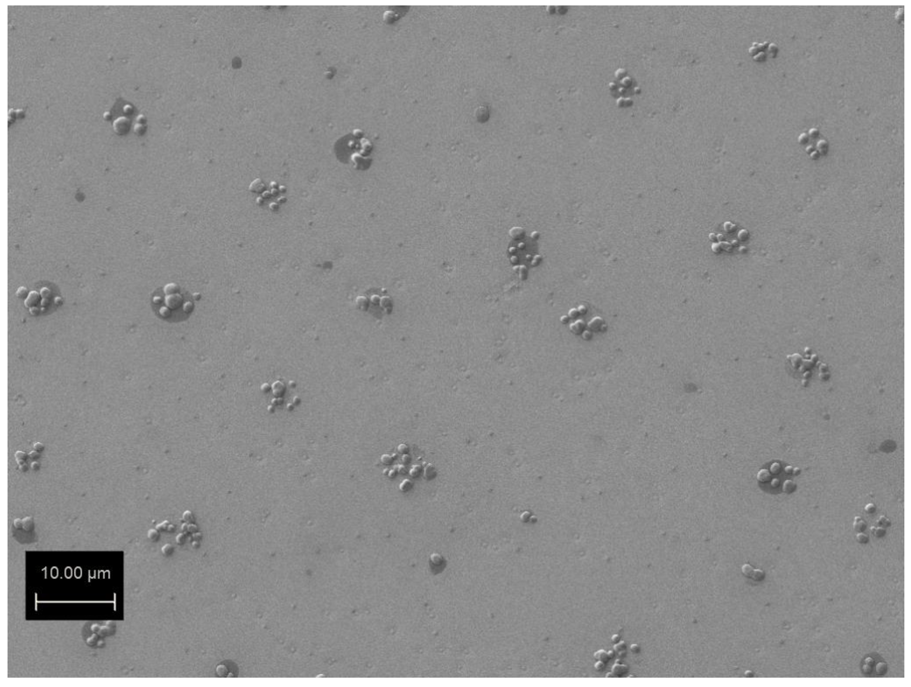
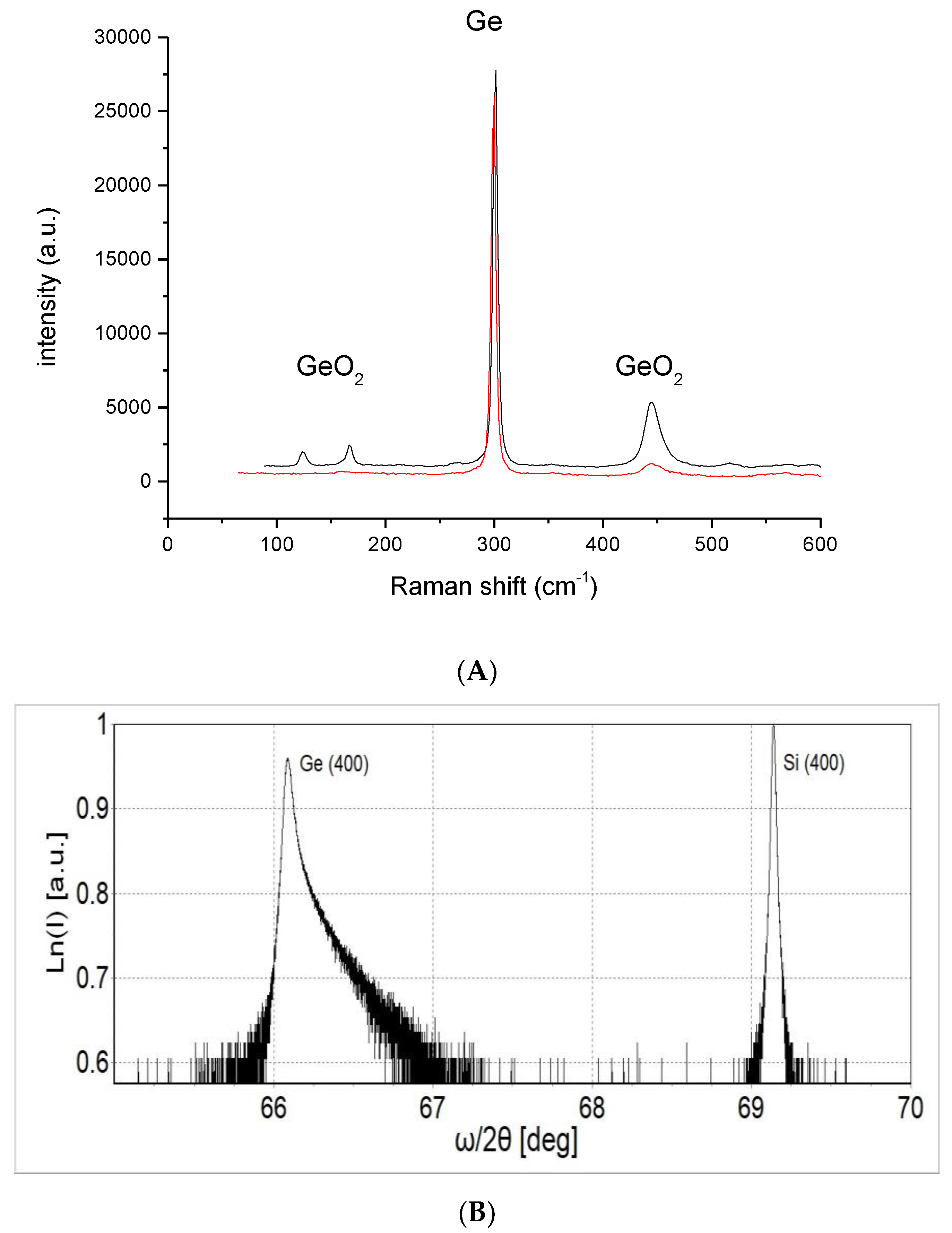
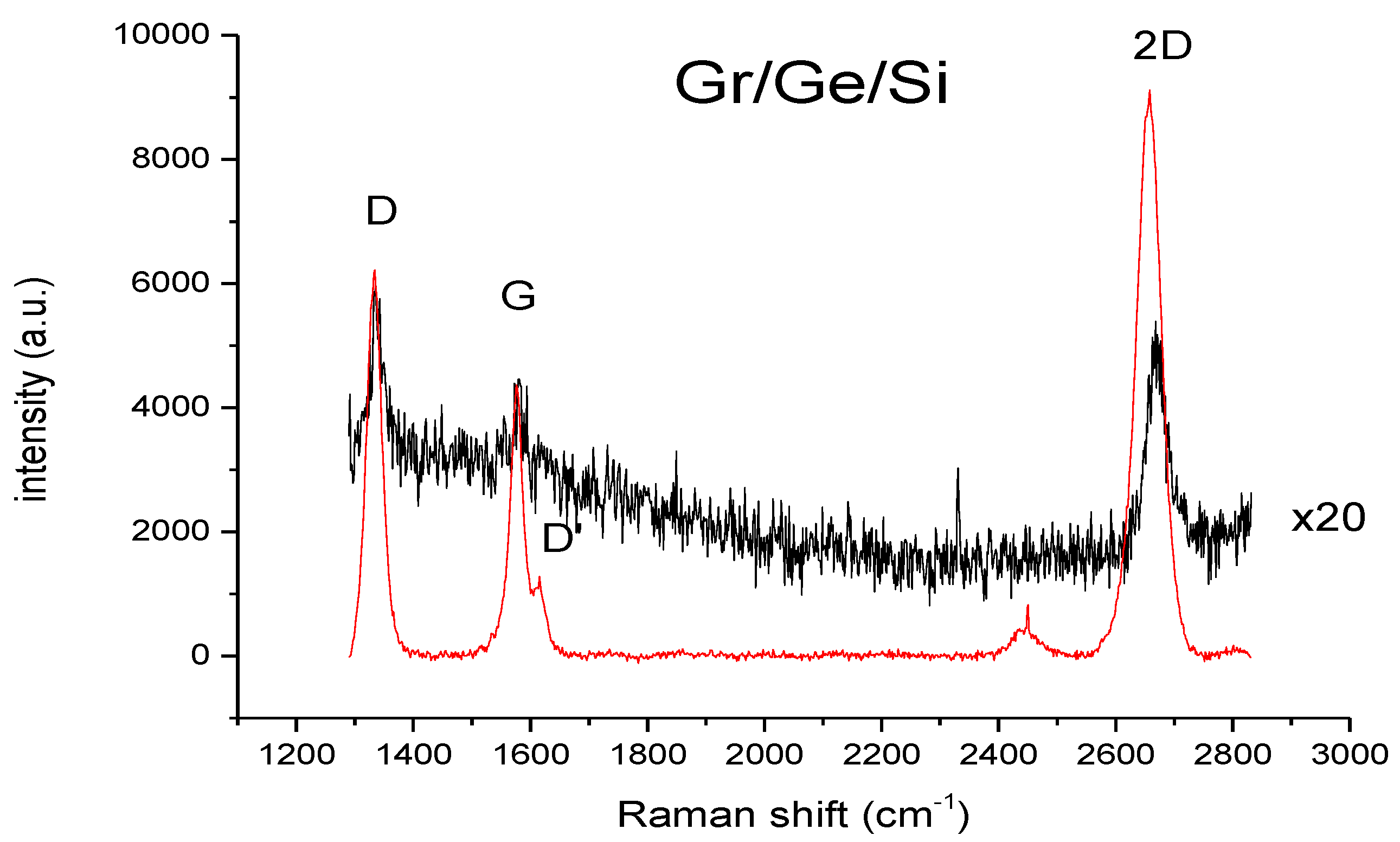
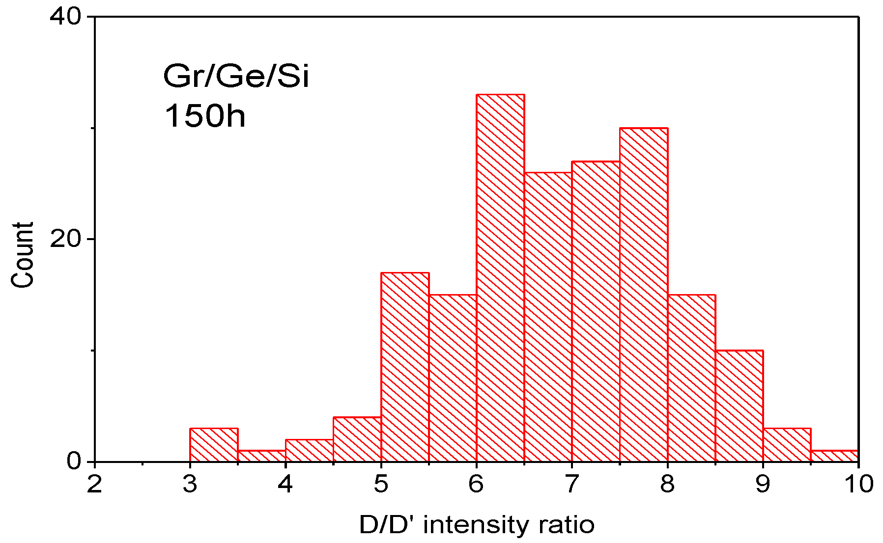
2. Methods and Results
3. Discussion
4. Conclusions
Author Contributions
Funding
Institutional Review Board Statement
Informed Consent Statement
Data Availability Statement
Acknowledgments
Conflicts of Interest
Sample Availability
References
- Di Gaspare, L.; Scaparro, A.; Fanfoni, M.; Fazi, L.; Sgarlata, A.; Notargiacomo, A.; Miseikis, V.; Coletti, C.; De Seta, M. Early stage of CVD graphene synthesis on Ge(001) substrate. Carbon 2018, 134, 183–188. [Google Scholar] [CrossRef]
- Dai, J.; Wang, D.; Zhang, M.; Niu, T.; Li, A.; Ye, M.; Guqiao, D.; Ding, G.; Xie, X.; Wang, Y.; et al. How Graphene Islands Are Unidirectionally Aligned on the Ge(110) Surface. Nano Lett. 2016, 16, 3160–3165. [Google Scholar] [CrossRef]
- Dabrowski, J.; Lippert, G.; Avila, J.; Baringhaus, J.; Colambo, I.; Dedkov, Y.; Herziger, F.; Lupina, G.; Maultzsch, J.; Schaffus, T.; et al. Understanding the growth mechanism of graphene on Ge/Si(001) surfaces. Sci. Rep. 2016, 6, 31639. [Google Scholar] [CrossRef] [Green Version]
- Wang, G.; Zhang, M.; Zhu, Y.; Ding, G.; Jiang, D.; Guo, Q.; Liu, S.; Xie, X.; Chu, P.K.; Di, Z.; et al. Direct Growth of Graphene Film on Germanium Substrate. Sci. Rep. 2013, 3, 2465. [Google Scholar] [CrossRef]
- Lee, J.-H.; Lee, E.K.; Joo, W.-J.; Jang, Y.; Kim, B.-S.; Lim, J.Y.; Choi, S.-H.; Ahn, S.J.; Ahn, J.R.; Park, M.-H.; et al. Wafer-Scale Growth of Single-Crystal Monolayer Graphene on Reusable Hydrogen-Terminated Germanium. Science 2014, 344, 286–289. [Google Scholar] [CrossRef] [PubMed]
- Lippert, G.; Dąbrowski, J.; Schroeder, T.; Schubert, M.A.; Yamamoto, Y.; Herziger, F.; Maultzsch, J.; Baringhaus, J.; Tegenkamp, C.; Asensio, M.C.; et al. Graphene grown on Ge(0 0 1) from atomic source. Carbon 2014, 75, 104–112. [Google Scholar] [CrossRef] [Green Version]
- Pasternak, I.; Wesolowski, M.; Jozwik, I.; Lukosius, M.; Lupina, G.; Dabrowski, P.; Baranowski, J.M.; Strupinski, W. Graphene growth on Ge(100)/Si(100) substrates by CVD method. Sci. Rep. 2016, 6, 21773. [Google Scholar] [CrossRef] [PubMed]
- Jacobberger, R.M.; Kiraly, B.; Fortin-Deschenes, M.; Levesque, P.; McElhinny, K.M.; Brady, G.J.; Delgado, R.R.; Roy, S.S.; Mannix, A.; Lagally, M.G.; et al. Direct oriented growth of armchair graphene nanoribbons on germanium. Nat. Commun. 2015, 6, 8006. [Google Scholar] [CrossRef]
- Kiraly, B.; Jacobberger, R.M.; Mannix, A.J.; Campbell, G.P.; Bedzyk, M.J.; Arnold, M.S.; Hersam, M.C.; Guisinger, N.P. Elec-tronic and Mechanical Properties of Graphene–Germanium Interfaces Grown by Chemical Vapor Deposition. Nano Lett. 2015, 15, 7. [Google Scholar] [CrossRef]
- Persichetti, L.; di Gaspare, L.; Fabbri, F.; Scaparro, A.M.; Notargiacomo, A.; Sgarlata, A.; Fanfoni, M.; Coletti, C.; de Seta, M. Abrupt changes in the graphene on Ge(001) system at the onset of surface melting. Carbon 2019, 145, 345. [Google Scholar] [CrossRef] [Green Version]
- Pasternak, I.; Dabrowski, P.; Ciepielewski, P.; Kolkovsky, V.; Klusek, Z.; Baranowski, J.M.; Strupinski, W. Large-area high-quality graphene on Ge(001)/Si(001) substrates. Nanoscale 2016, 8, 11241–11247. [Google Scholar] [CrossRef]
- Braeuninger-Weimer, P.; Burton, O.; Weatherup, R.S.; Wang, R.; Dudin, P.; Brennan, B.; Pollard, A.J.; Bayer, B.C.; Veigang-Radulescu, V.P.; Meyer, J.C.; et al. Reactive intercalation and oxidation at the buried graphene-germanium interface. APL Mater. 2019, 7, 071107. [Google Scholar] [CrossRef] [Green Version]
- Judek, J.; Pasternak, I.; Dabrowski, P.; Strupinski, W.; Zdrojek, M. Hydrogen intercalation of CVD graphene on germanium (001)–Strain and doping analysis using Raman spectroscopy. Appl. Surf. Sci. 2018, 473, 203–208. [Google Scholar] [CrossRef]
- McElhinny, K.M.; Jacobberger, R.M.; Zaug, A.J.; Arnold, M.S.; Evans, P.G. Graphene-induced Ge (001) surface faceting. Surf. Sci. 2016, 647, 90–95. [Google Scholar] [CrossRef] [Green Version]
- Dabrowski, P.; Rogala, M.; Pasternak, I.; Krukowski, P.; Baranowski, J.; Strupinski, W.; Lutsyk, I.; Kowalczyk, D.; Pawłowski, S.; Klusek, Z. Early oxidation stages of germanium substrate in the graphene/Ge(001) system. Carbon 2019, 149, 290–296. [Google Scholar] [CrossRef]
- Akhtar, F.; Dabrowski, J.; Lisker, M.; Yamamoto, Y.; Mai, A.; Wenger, C.; Lukosius, M. Investigation of the Oxidation Behavior of Graphene/Ge(001) Versus Graphene/Ge(110) Systems. ACS Appl. Mater. Interfaces 2020, 12, 3188–3197. [Google Scholar] [CrossRef] [PubMed]
- Binder, J.; Rogoza, J.; Tkachenko, L.; Pasternak, I.; Sitek, J.; Strupinskii, W.; Zdrojek, M.; Baranowski, J.M.; Stępniewski, R.; Wysmołek, A. Suspended graphene on germanium: Selective local etching via laser-induced photocorrosion of germanium. 2D Mater. 2021, 8, 13. [Google Scholar] [CrossRef]
- Liu, Q.-J.; Liu, Z.-T. Structural, elastic, and mechanical properties of germanium dioxide from first-principles calculations. Mater. Sci. Semicond. Process. 2014, 27, 765–776. [Google Scholar] [CrossRef]
- Khan, M.A.; Hogan, T.P.; Shanker, B. Surface-enhanced Raman scattering from gold-coated germa-nium oxide nanowires. J. Raman. Spectrosc. 2008, 39, 893–900. [Google Scholar] [CrossRef]
- Ferrari, A.C.; Basko, D.M. Raman spectroscopy as a versatile tool for studying the properties of graphene. Nat. Nanotechnol. 2013, 8, 235–246. [Google Scholar] [CrossRef] [PubMed] [Green Version]
- Eckmann, A.; Felten, A.; Mishchenko, A.; Britnell, L.; Krupke, R.; Novoselov, K.S.; Casiraghi, C. Probing the Nature of Defects in Graphene by Raman Spectroscopy. Nano Lett. 2012, 12, 3925–3930. [Google Scholar] [CrossRef] [PubMed] [Green Version]
- Lazzeri, M.; Mauri, F. Nonadiabatic Kohn Anomaly in a Doped Graphene Monolayer. Phys. Rev. Lett. 2006, 97, 266407. [Google Scholar] [CrossRef] [PubMed] [Green Version]
- Neumann, C.; Teichardd, S.; Venezuala, P.; Drogeler, M.; Banszerus, L.; Schmitz, M.; Watanabe, K.; Taniguchi, T.; Mauri, F.; Beschoten, B.; et al. Raman spectroscopy as probe of nanometer-scale strain variations in graphene. Nat. Commun. 2015, 6, 8429. [Google Scholar] [CrossRef] [Green Version]
- Lee, J.E.; Ahn, G.; Shim, J.; Lee, Y.S.; Ryu, S. Optical separation of mechanical strain from charge doping in graphene. Nat. Commun. 2012, 3, 1024. [Google Scholar] [CrossRef] [Green Version]
- Das, A.; Pisana, S.; Chakraborty, B.; Piscanec, S.; Saha, S.K.; Waghmare, U.V.; Novoselov, K.S.; Krishnamurthy, H.R.; Geim, A.K.; Ferrari, A.C.; et al. Monitoring dopants by Raman scattering in an electrochemically top-gated graphene transistor. Nat. Nanotechnol. 2008, 3, 210–215. [Google Scholar] [CrossRef] [Green Version]
- Politano, A.; Marino, A.R.; Formoso, V.; Chiarello, G. Water adsorption on graphene/Pt(111) at room temperature: A vibrational investigation. AIP Adv. 2011, 1, 042130. [Google Scholar] [CrossRef] [Green Version]
- Mohiuddin, T.M.G.; Lombardo, A.; Nair, R.R.; Bonetti, A.; Savini, G.; Jalil, R.; Bonini, N.; Basko, D.M.; Galiotis, C.; Marzari, N.; et al. Uniaxial strain in graphene by Raman spectroscopy: G peak splitting. Grüneisen parameters, and sample orientation. Phys. Rev. B Condens. Matter 2009, 79, 205433. [Google Scholar] [CrossRef]
- Schriver, M.; Regan, W.; Gannett, W.J.; Zaniewski, A.M.; Crommie, M.F.; Zettl, A. Graphene as a Long-Term Metal Oxidation Barrier: Worse Than Nothing. ACS Nano 2013, 7, 5763–5768. [Google Scholar] [CrossRef]
- Zhou, F.; Li, Z.; Shenoy, G.J.; Li, L.; Liu, H. Enhanced Room-Temperature Corrosion of Copper in the Presence of Graphene. ACS Nano 2013, 7, 6939–6947. [Google Scholar] [CrossRef]
- Stockman, M.I. Nanoplasmonics: Past, present, and glimpse into future. Opt. Express 2011, 19, 22029–22106. [Google Scholar] [CrossRef] [Green Version]
- Garcia, M.A. Surface plasmons in metallic nanoparticles: Fundamentals and applications. J. Phys. D Appl. Phys. 2012, 45, 389501. [Google Scholar] [CrossRef] [Green Version]
- West, P.; Ishii, S.; Naik, G.; Emani, N.K.; Shalaev, V.; Boltasseva, A. Searching for better plasmonic materials. Laser Photon. Rev. 2010, 4, 795–808. [Google Scholar] [CrossRef] [Green Version]
- McMahon, J.M.; Schatz, G.C.; Gray, S.K. Plasmonics in the ultraviolet with the poor metals Al, Ga, In, Sn, Tl, Pb, and Bi. Phys. Chem. Chem. Phys. 2013, 15, 5415–5423. [Google Scholar] [CrossRef]
- Yazyev, O.V.; Louie, S.G. Electronic transport in polycrystalline graphene. Nat. Mater. 2010, 9, 806. [Google Scholar] [CrossRef] [Green Version]


Publisher’s Note: MDPI stays neutral with regard to jurisdictional claims in published maps and institutional affiliations. |
© 2022 by the authors. Licensee MDPI, Basel, Switzerland. This article is an open access article distributed under the terms and conditions of the Creative Commons Attribution (CC BY) license (https://creativecommons.org/licenses/by/4.0/).
Share and Cite
Dumiszewska, E.; Ciepielewski, P.; Caban, P.A.; Jóźwik, I.; Gaca, J.; Baranowski, J.M. Formation of GeO2 under Graphene on Ge(001)/Si(001) Substrates Using Water Vapor. Molecules 2022, 27, 3636. https://doi.org/10.3390/molecules27113636
Dumiszewska E, Ciepielewski P, Caban PA, Jóźwik I, Gaca J, Baranowski JM. Formation of GeO2 under Graphene on Ge(001)/Si(001) Substrates Using Water Vapor. Molecules. 2022; 27(11):3636. https://doi.org/10.3390/molecules27113636
Chicago/Turabian StyleDumiszewska, Ewa, Paweł Ciepielewski, Piotr A. Caban, Iwona Jóźwik, Jaroslaw Gaca, and Jacek M. Baranowski. 2022. "Formation of GeO2 under Graphene on Ge(001)/Si(001) Substrates Using Water Vapor" Molecules 27, no. 11: 3636. https://doi.org/10.3390/molecules27113636
APA StyleDumiszewska, E., Ciepielewski, P., Caban, P. A., Jóźwik, I., Gaca, J., & Baranowski, J. M. (2022). Formation of GeO2 under Graphene on Ge(001)/Si(001) Substrates Using Water Vapor. Molecules, 27(11), 3636. https://doi.org/10.3390/molecules27113636