
Environment-Induced Reversible Modulation of Optical and Electronic Properties of Lead Halide Perovskites and Possible Applications to Sensor Development: A Review


Abstract
1. Introduction
2. Environmental Stability of Perovskites
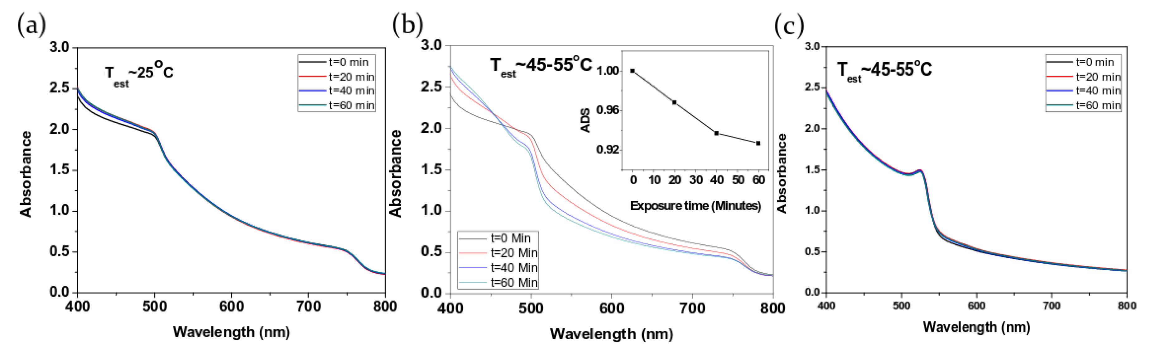
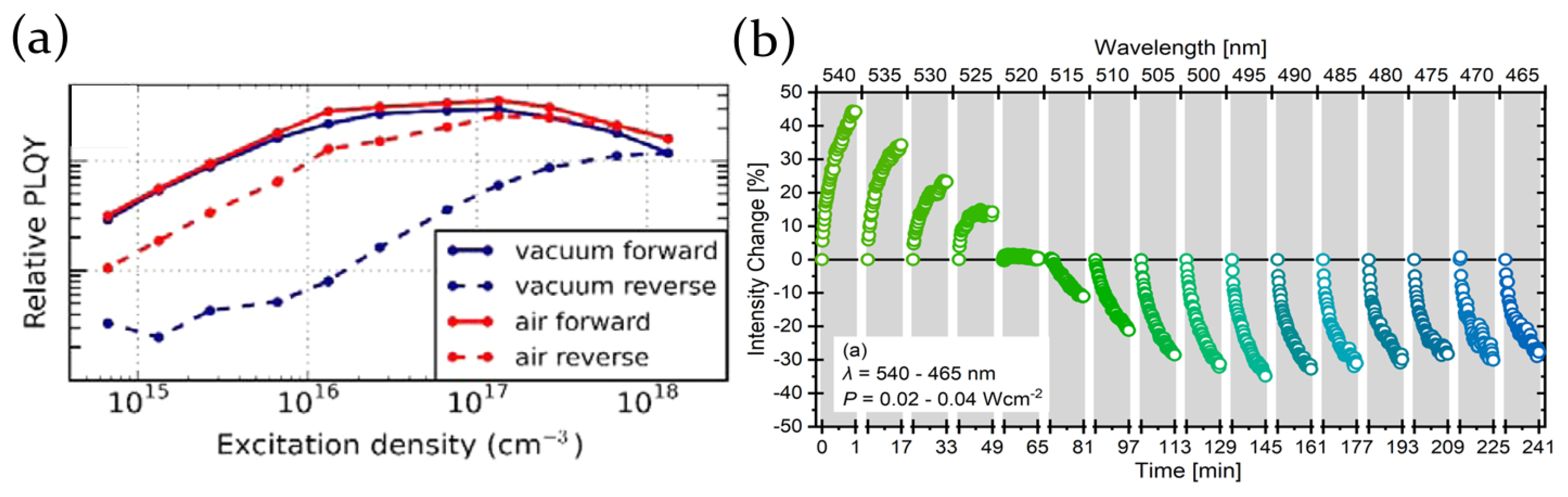
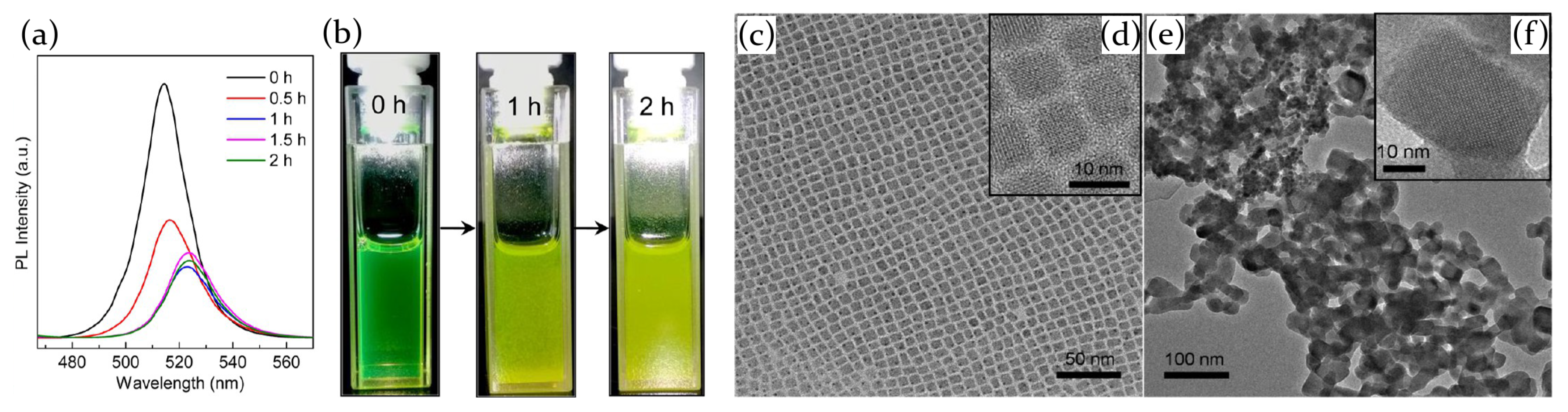
2.1. Light and Temperature Effects
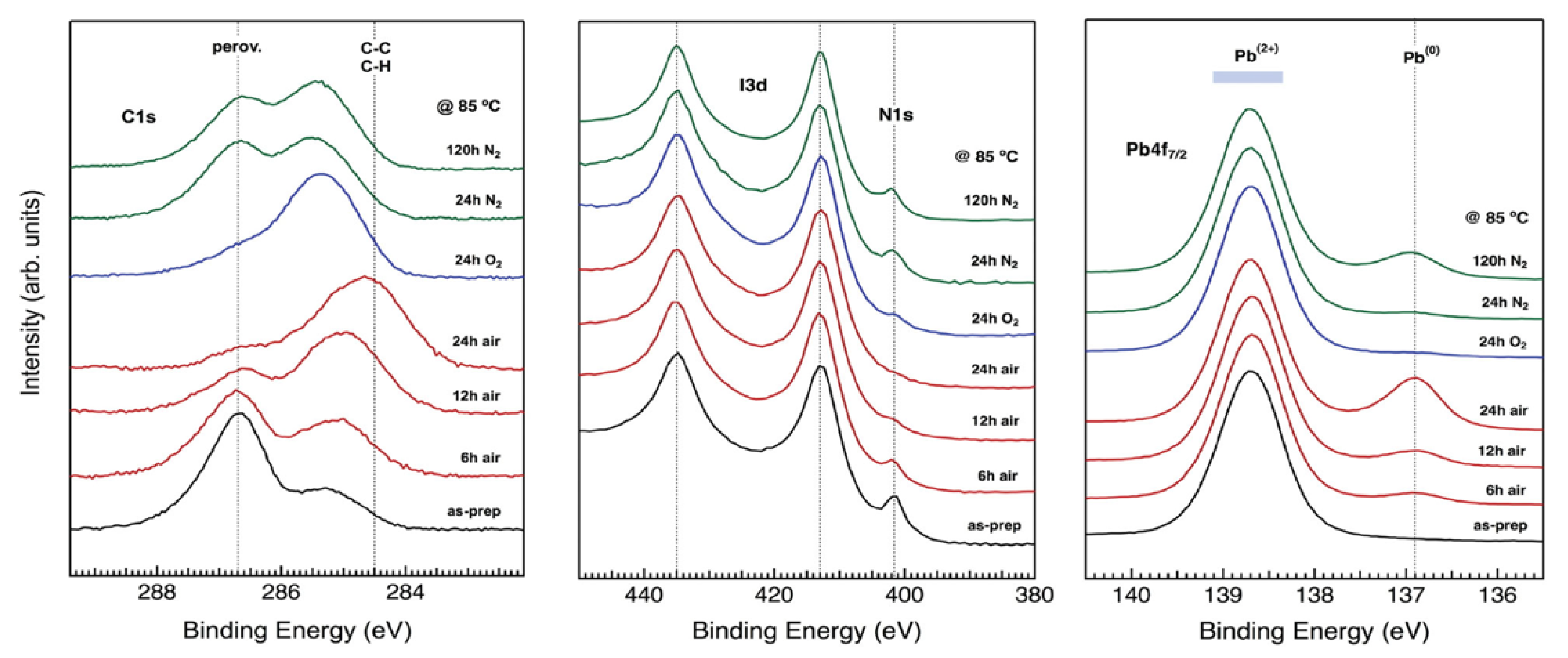
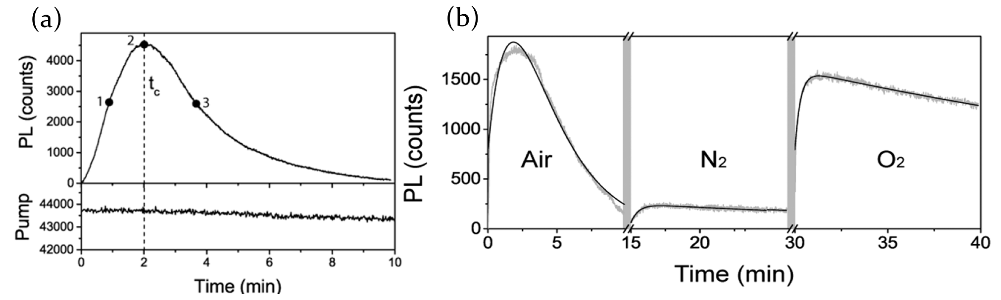
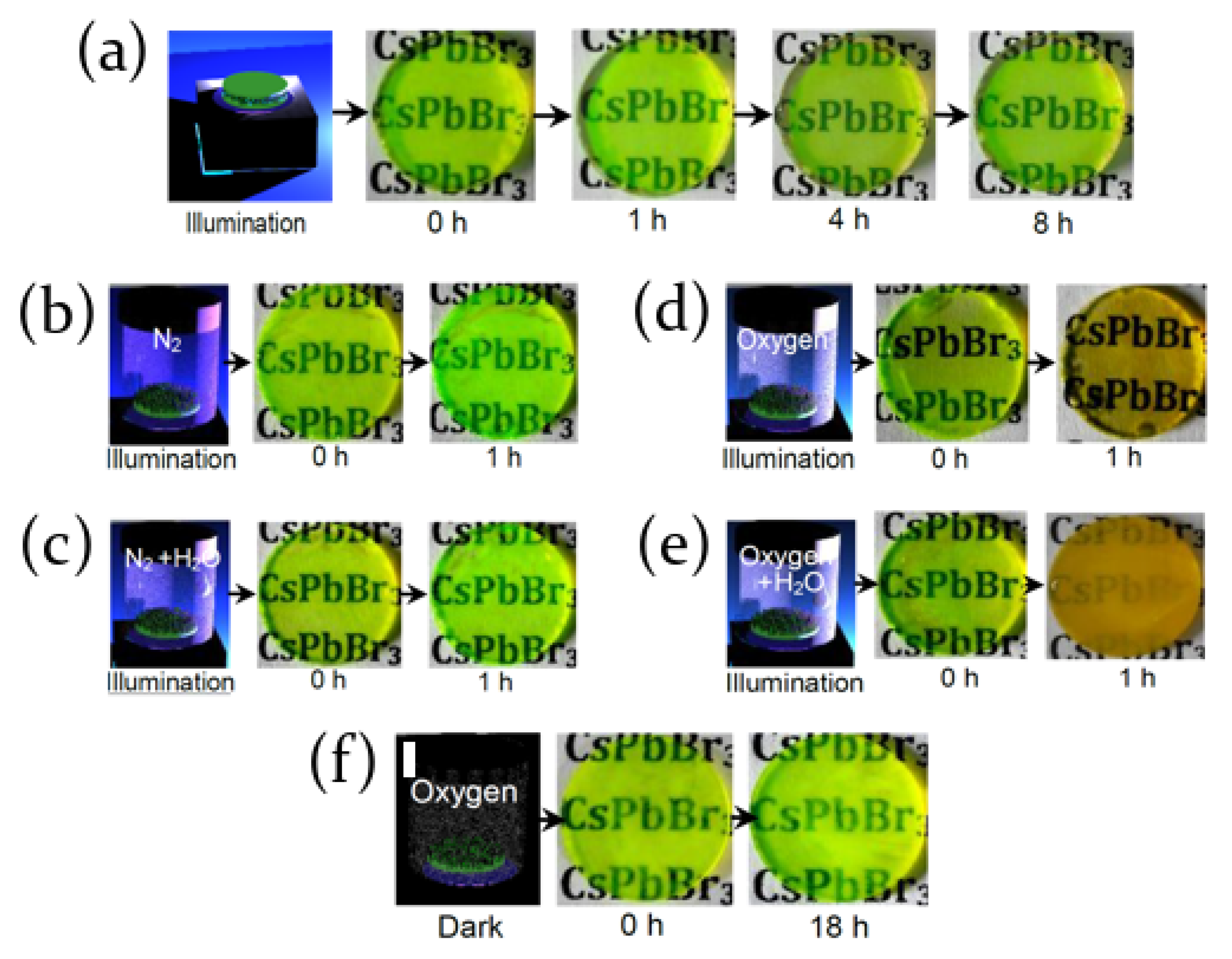
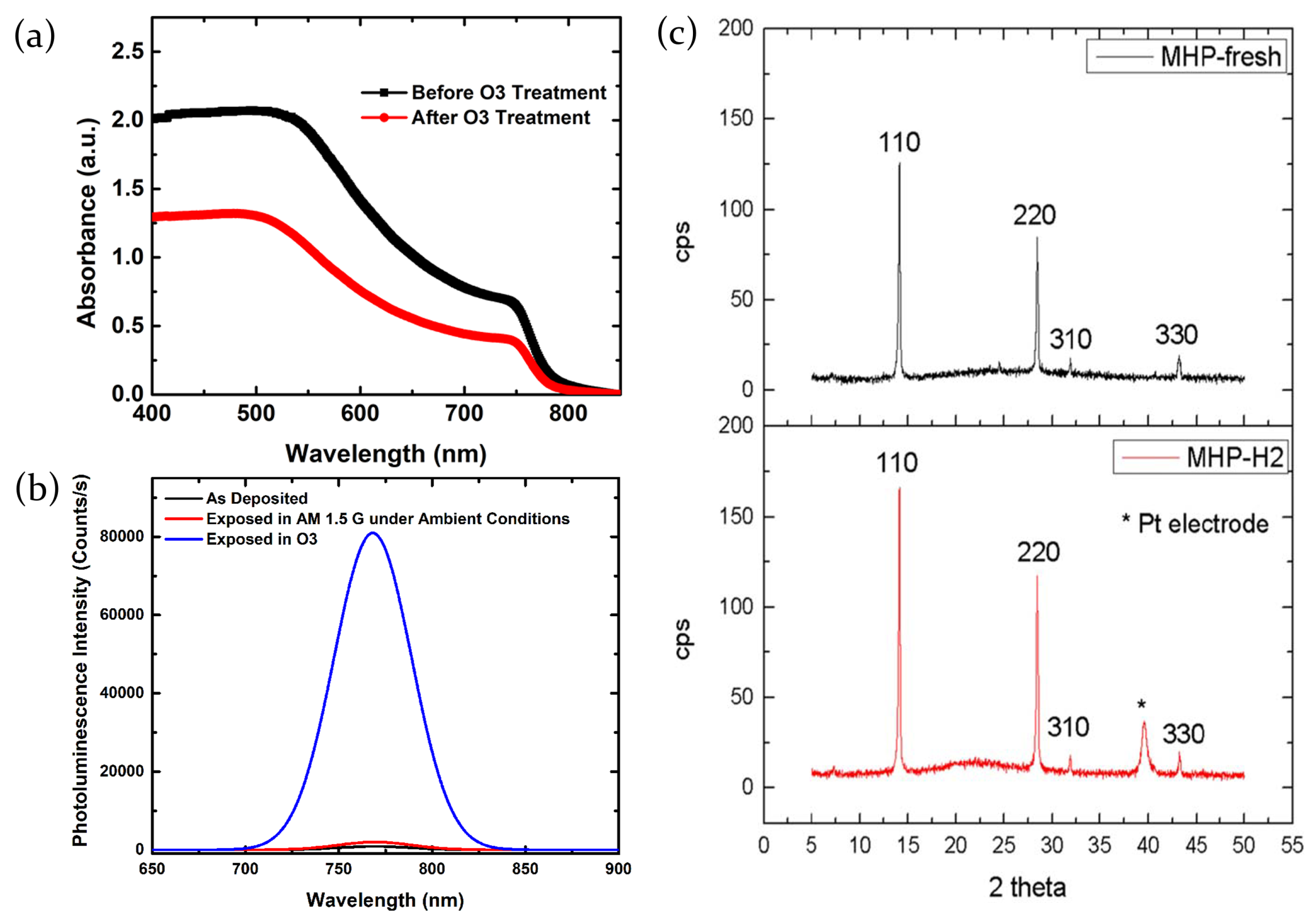
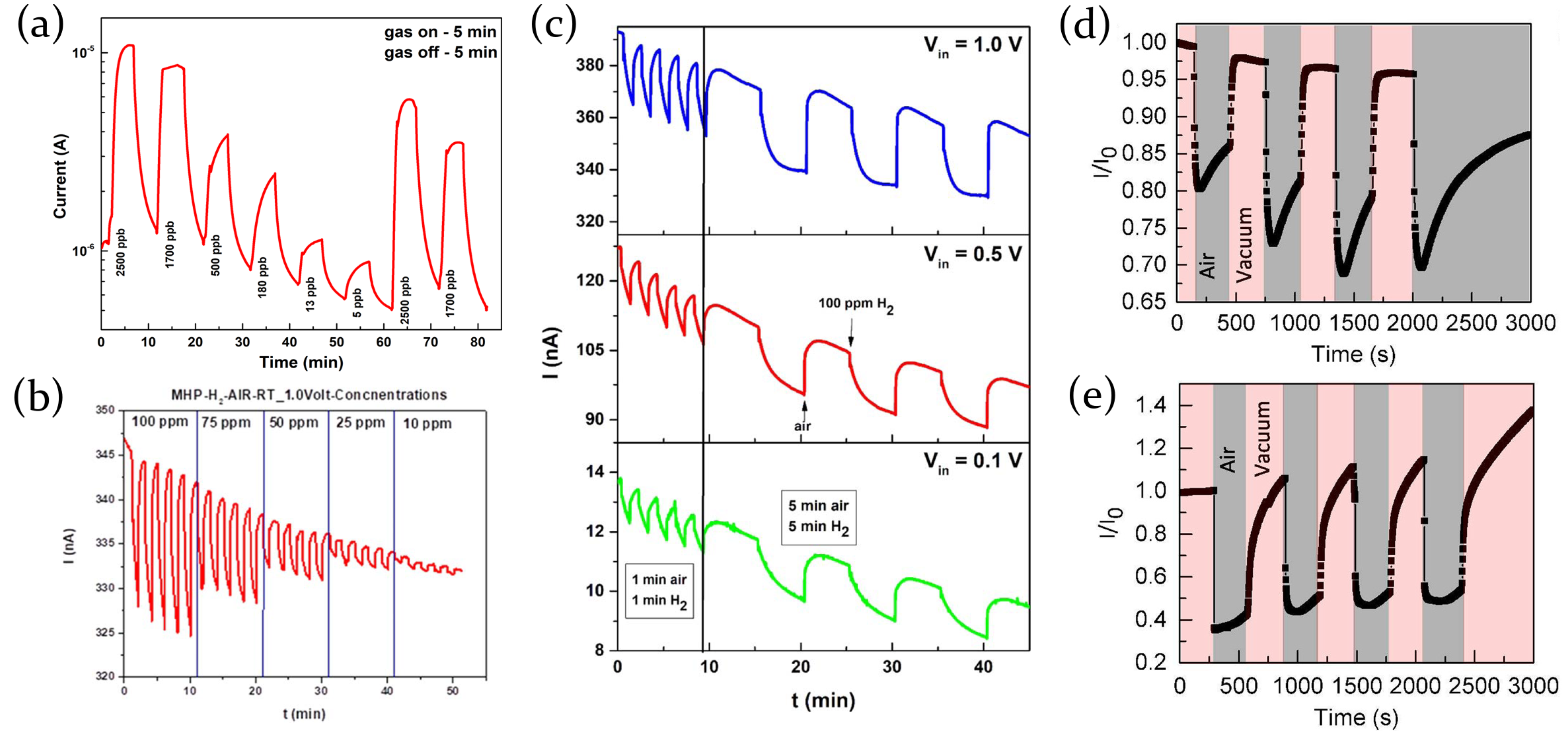
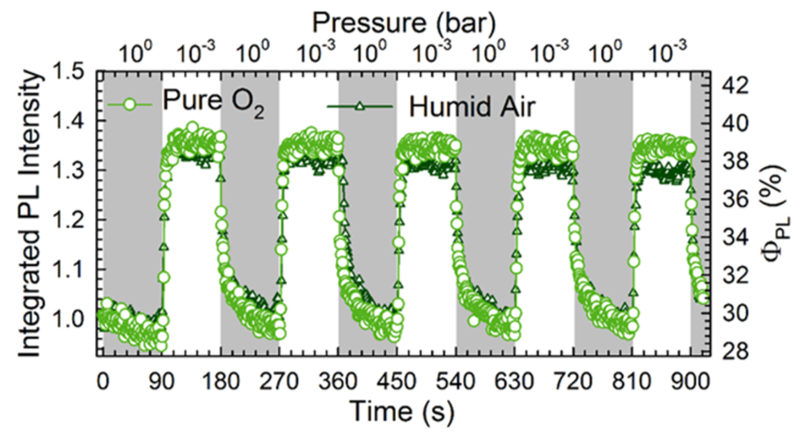
2.2. Air, Oxygen and Humidity Effects
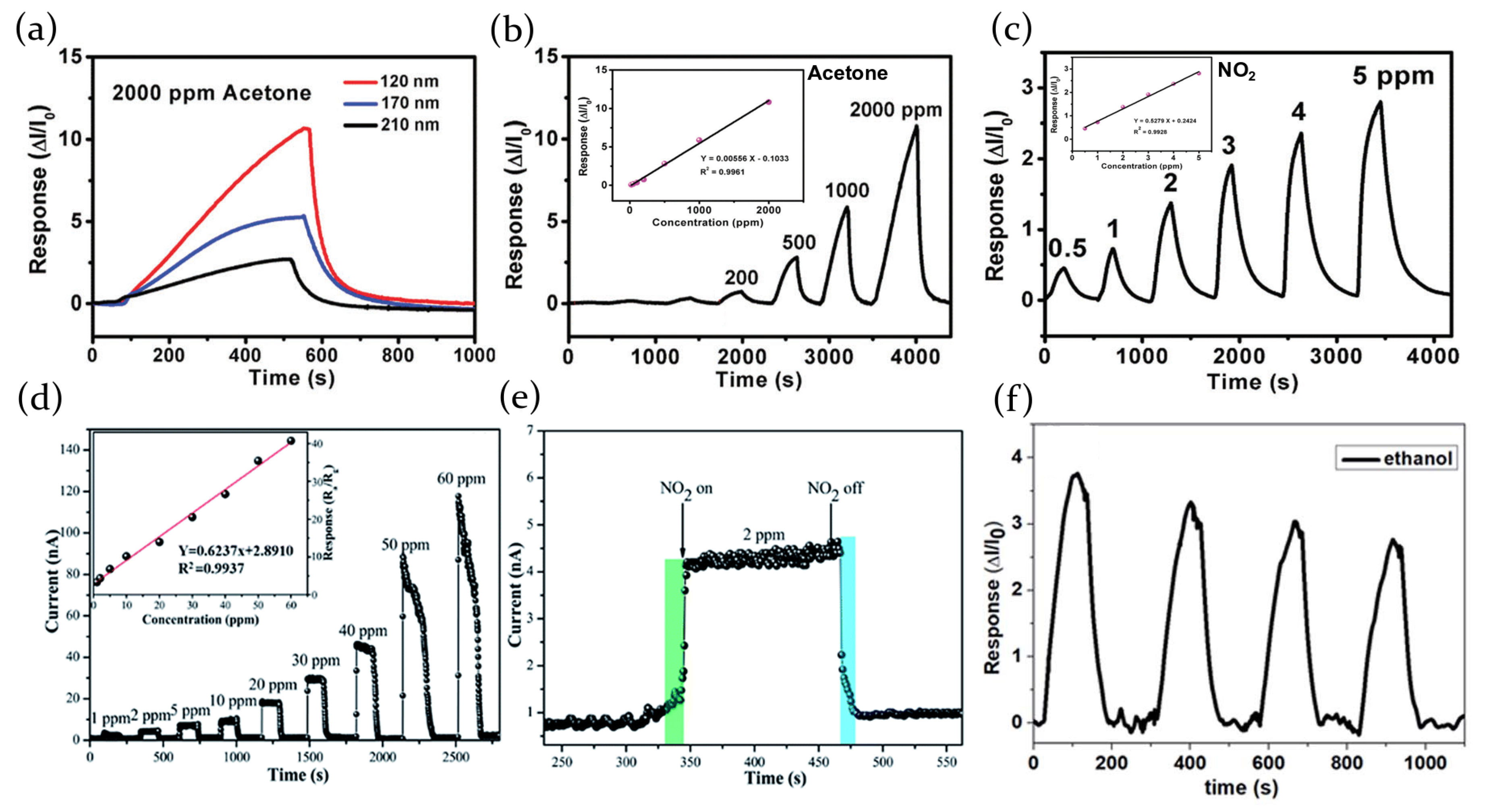
2.3. Gas Atmosphere Effects ( , , VOC, , )
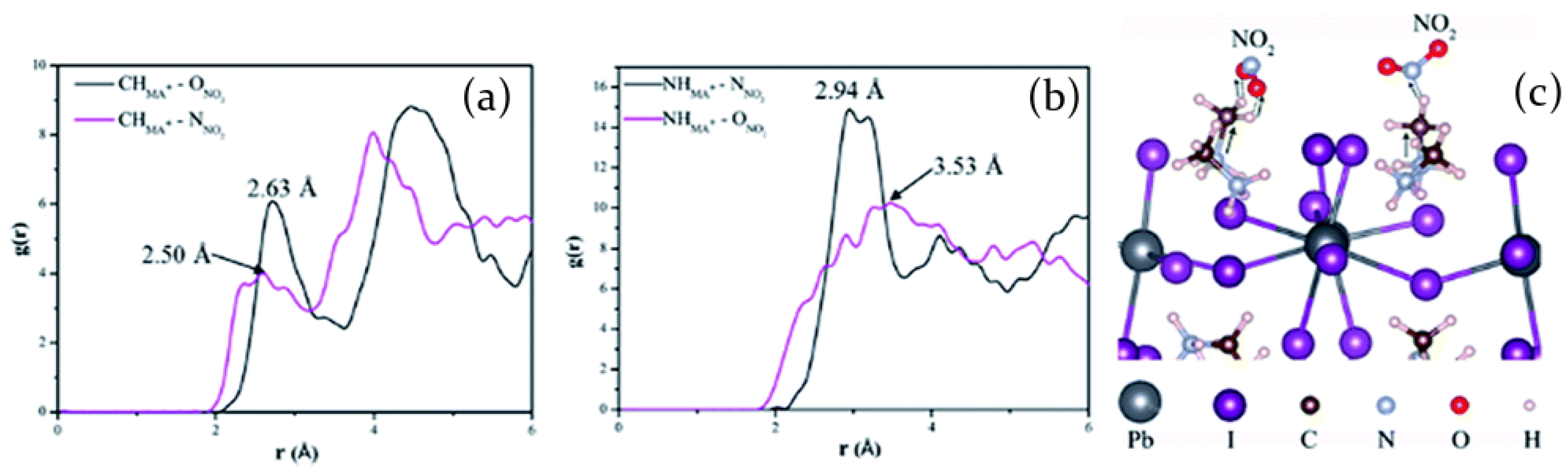
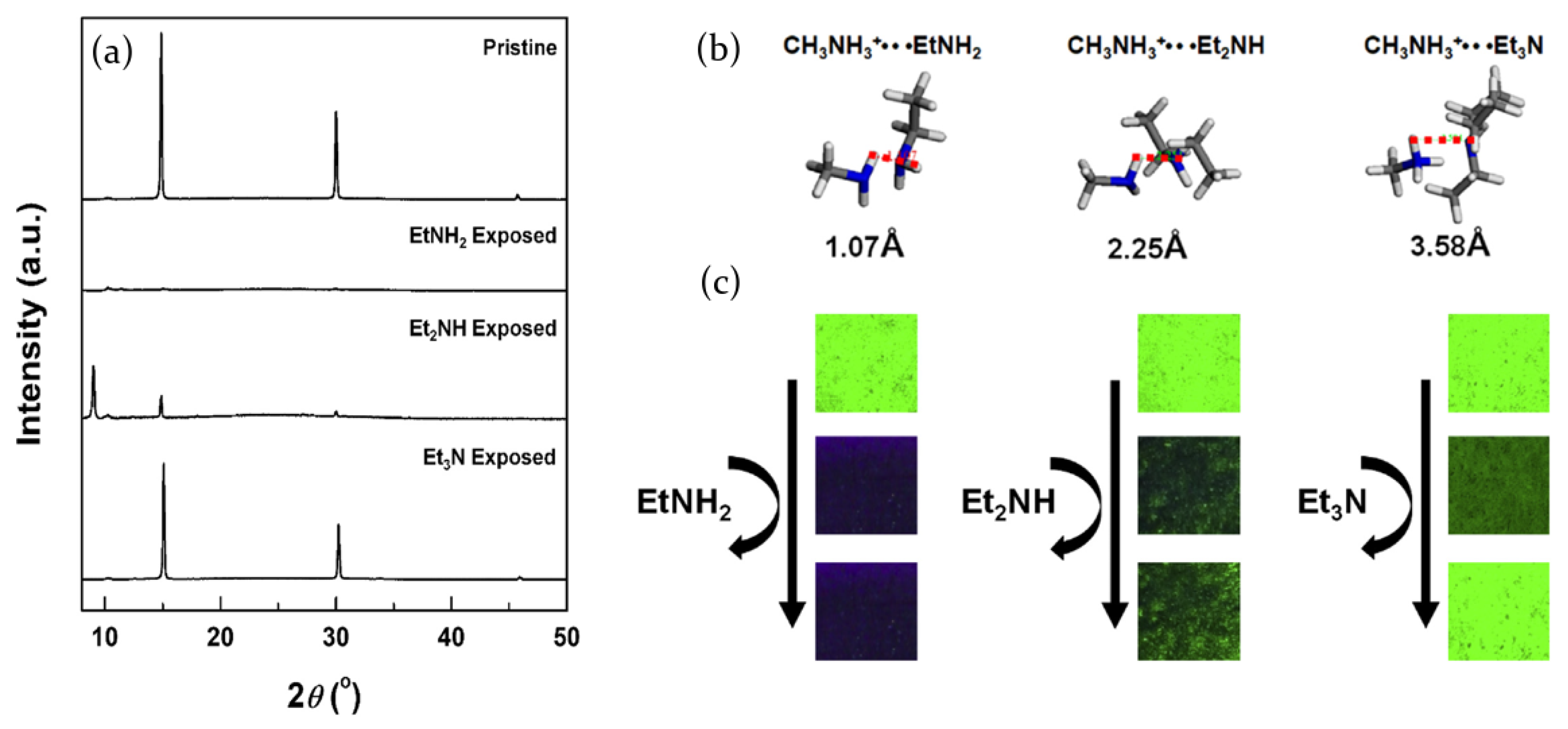
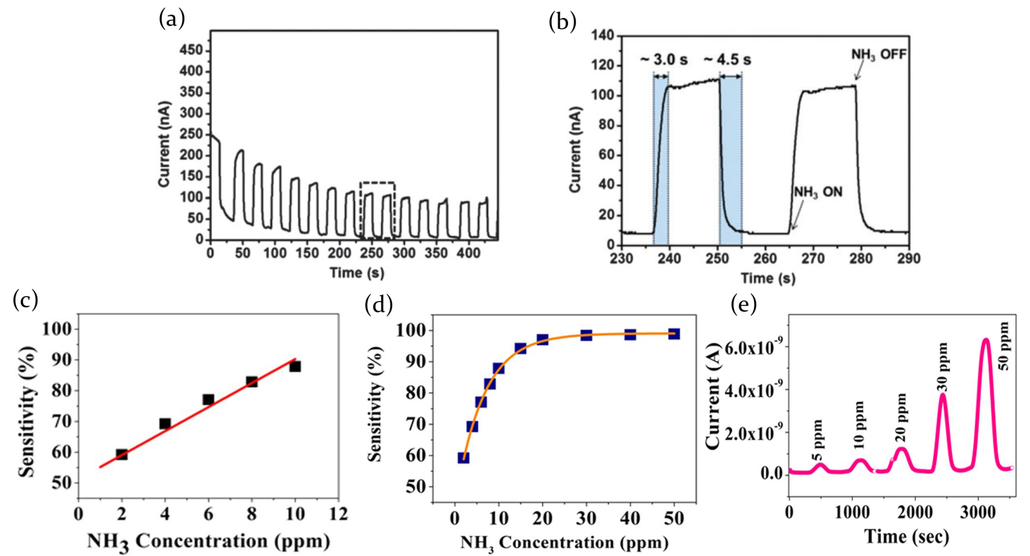
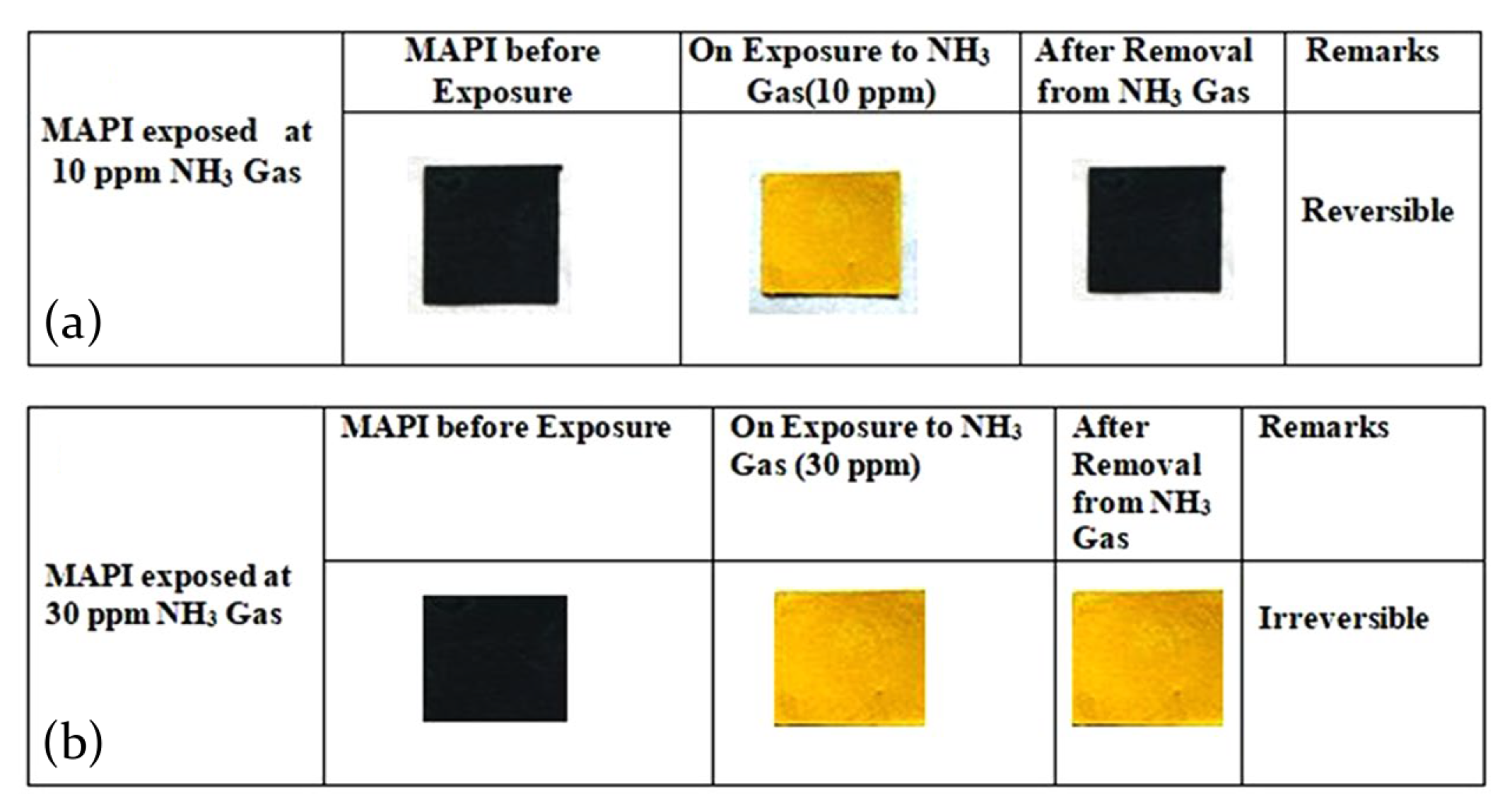
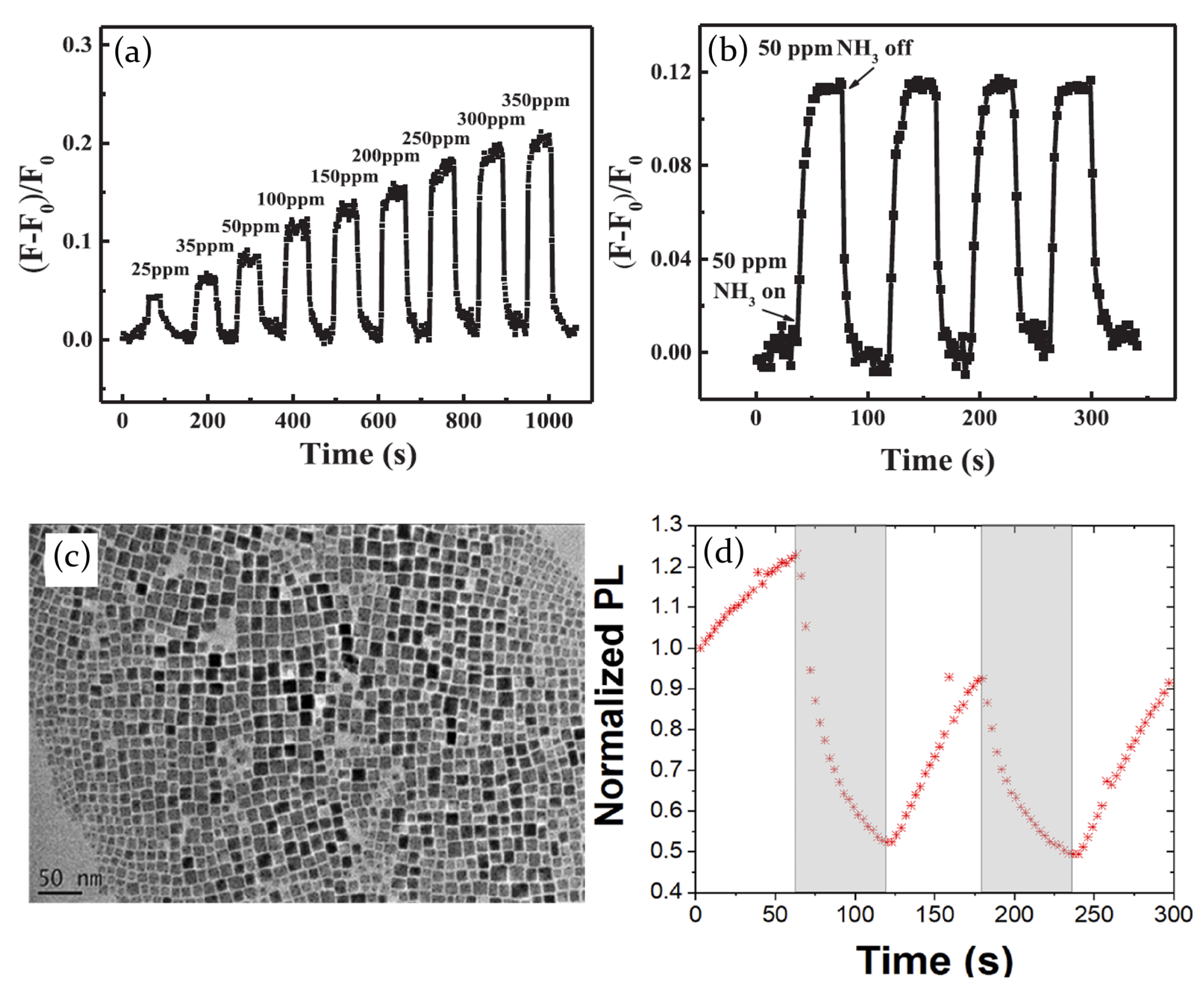
2.3.1. Ammonia
2.3.2. Nitrogen Dioxide
2.3.3. Volatile Organic Compound
2.3.4. Ozone
2.3.5. Hydrogen
3. Sensing Application of Perovskites
3.1. Resistive Sensors
3.2. Optical Sensors
3.2.1. Color Change Gas Sensor
3.2.2. PL Emission-Based Gas Sensors
4. Perspectives
Author Contributions
Funding
Institutional Review Board Statement
Informed Consent Statement
Conflicts of Interest
References
- Sun, Y.F.; Liu, S.B.; Meng, F.L.; Liu, J.Y.; Jin, Z.; Kong, L.T.; Liu, J.H. Metal Oxide Nanostructures and Their Gas Sensing Properties: A Review. Sensors 2012, 12, 2610–2631. [Google Scholar] [CrossRef] [PubMed]
- Chiu, S.W.; Tang, K.T. Towards a Chemiresistive Sensor-Integrated Electronic Nose: A Review. Sensors 2013, 13, 14214–14247. [Google Scholar] [CrossRef] [PubMed]
- Gupta Chatterjee, S.; Chatterjee, S.; Ray, A.K.; Chakraborty, A.K. Graphene–metal oxide nanohybrids for toxic gas sensor: A review. Sens. Actuators B 2015, 221, 1170–1181. [Google Scholar] [CrossRef]
- Zhu, L.; Zeng, W. Room-temperature gas sensing of ZnO-based gas sensor: A review. Sens. Actuators A 2017, 267, 242–261. [Google Scholar] [CrossRef]
- Nazemi, H.; Joseph, A.; Park, J.; Emadi, A. Advanced Micro- and Nano-Gas Sensor Technology: A Review. Sensors 2019, 19, 1285. [Google Scholar] [CrossRef] [PubMed]
- Arafat, M.M.; Dinan, B.; Akbar, S.A.; Haseeb, A.S.M.A. Gas Sensors Based on One Dimensional Nanostructured Metal-Oxides: A Review. Sensors 2012, 12, 7207–7258. [Google Scholar] [CrossRef] [PubMed]
- Nur’aini, A.; Oh, I. Volatile organic compound gas sensors based on methylammonium lead iodide perovskite operating at room temperature. RSC Adv. 2020, 10, 12982–12987. [Google Scholar] [CrossRef]
- Gagaoudakis, E.; Panagiotopoulos, A.; Maksudov, T.; Moschogiannaki, M.; Katerinopoulou, D.; Kakavelakis, G.; Kiriakidis, G.; Binas, V.; Kymakis, E.; Petridis, K. Self-powered, flexible and room temperature operated solution processed hybrid metal halide p-type sensing element for efficient hydrogen detection. J. Phys. Mater. 2020, 3, 014010. [Google Scholar] [CrossRef]
- Zhao, Y.; Zhu, K. Organic-inorganic hybrid lead halide perovskites for optoelectronic and electronic applications. Chem. Soc. Rev. 2016, 45, 655–689. [Google Scholar] [CrossRef]
- Protesescu, L.; Yakunin, S.; Bodnarchuk, M.I.; Krieg, F.; Caputo, R.; Hendon, C.H.; Yang, R.X.; Walsh, A.; Kovalenko, M.V. Nanocrystals of Cesium Lead Halide Perovskites (CsPbX3, X = Cl, Br, and I): Novel Optoelectronic Materials Showing Bright Emission with Wide Color Gamut. Nano Lett. 2015, 15, 3692–3696. [Google Scholar] [CrossRef]
- Deschler, F.; Price, M.; Pathak, S.; Klintberg, L.E.; Jarausch, D.D.; Higler, R.; Hüttner, S.; Leijtens, T.; Stranks, S.D.; Snaith, H.J.; et al. High Photoluminescence Efficiency and Optically Pumped Lasing in Solution-Processed Mixed Halide Perovskite Semiconductors. J. Phys. Chem. Lett. 2014, 5, 1421–1426. [Google Scholar] [CrossRef] [PubMed]
- Brenner, T.; Egger, D.; Kronik, L.; Hodes, G.; Cahen, D. Hybrid Organic-Inorganic Perovskites: Low-Cost Semiconductors with Intriguing Charge-Transport Properties. Nat. Rev. Mater. 2016, 1, 15007. [Google Scholar] [CrossRef]
- Stoumpos, C.C.; Malliakas, C.D.; Kanatzidis, M.G. Semiconducting tin and lead iodide perovskites with organic cations: Phase transitions, high mobilities, and near-infrared photoluminescent properties. Inorg. Chem. 2013, 52, 9019–9038. [Google Scholar] [CrossRef] [PubMed]
- Sutherland, B.R.; Hoogland, S.; Adachi, M.M.; Kanjanaboos, P.; Wong, C.T.; McDowell, J.J.; Xu, J.; Voznyy, O.; Ning, Z.; Houtepen, A.J.; et al. Perovskite thin films via atomic layer deposition. Adv. Mater. 2015, 27, 53–58. [Google Scholar] [CrossRef] [PubMed]
- Motti, S.G.; Krieg, F.; Ramadan, A.J.; Patel, J.B.; Snaith, H.J.; Kovalenko, M.V.; Johnston, M.B.; Herz, L.M. CsPbBr3 Nanocrystal Films: Deviations from Bulk Vibrational and Optoelectronic Properties. Adv. Funct. Mater. 2020, 30, 1909904. [Google Scholar] [CrossRef]
- De Giorgi, M.L.; Krieg, F.; Kovalenko, M.; Anni, M. Amplified Spontaneous Emission Threshold Reduction and Operational Stability Improvement in CsPbBr3 Nanocrystals Films by Hydrophobic Functionalization of the Substrate. Sci. Rep. 2019, 9. [Google Scholar] [CrossRef] [PubMed]
- Weber, D. CH3NH3PbX3, a Pb(II)-System with Cubic Perovskite Structure. Z. Naturforschung B 1978, 33, 1443–1445. [Google Scholar] [CrossRef]
- Weber, D. CH3NH3SnBrxI3−x (x=0–3), a Sn(II)-System with Cubic Perovskite Structure. Z. Naturforschung B 1978, 33, 862–865. [Google Scholar] [CrossRef]
- Kojima, A.; Teshima, K.; Shirai, Y.; Miyasaka, T. Organometal Halide Perovskites as Visible-Light Sensitizers for Photovoltaic Cells. J. Am. Chem. Soc. 2009, 131, 6050–6051. [Google Scholar] [CrossRef]
- Sun, S.; Salim, T.; Mathews, N.; Duchamp, M.; Boothroyd, C.; Xing, G.; Sum, T.C.; Lam, Y.M. The origin of high efficiency in low-temperature solution-processable bilayer organometal halide hybrid solar cells. Energy Environ. Sci. 2014, 7, 399–407. [Google Scholar] [CrossRef]
- Stranks, S.D.; Snaith, H. Metal-halide perovskites for photovoltaic and light-emitting devices. Nat. Nanotechnol. 2015, 10, 391–402. [Google Scholar] [CrossRef] [PubMed]
- National Renewable Energy Laboratory. Research Cell Record Efficiency Chart. Available online: https://www.nrel.gov/pv/cell-efficiency.html (accessed on 15 December 2020).
- Hattori, T.; Taira, T.; Era, M.; Tsutsui, T.; Saito, S. Highly efficient electroluminescence from a heterostructure device combined with emissive layered-perovskite and an electron-transporting organic compound. Chem. Phys. Lett. 1996, 254, 103–108. [Google Scholar] [CrossRef]
- Chondroudis, K.; Mitzi, D.B. Electroluminescence from an Organic-Inorganic Perovskite Incorporating a Quaterthiophene Dye within Lead Halide Perovskite Layers. Chem. Mater. 1999, 11, 3028–3030. [Google Scholar] [CrossRef]
- Kojima, A.; Ikegami, M.; Teshima, K.; Miyasaka, T. Highly Luminescent Lead Bromide Perovskite Nanoparticles Synthesized with Porous Alumina Media. Chem. Lett. 2012, 41, 397–399. [Google Scholar] [CrossRef]
- Tan, Z.; Moghaddam, R.; Lai, M.; Docampo, P.; Higler, R.; Deschler, F.; Price, M.; Sadhanala, A.; Pazos, L.; Credgington, D.; et al. Bright light-emitting diodes based on organometal halide perovskite. Nat. Nanotechnol. 2014, 9, 687–692. [Google Scholar] [CrossRef]
- Li, G.; Tan, Z.K.; Di, D.; Lai, M.L.; Jiang, L.; Lim, J.H.W.; Friend, R.H.; Greenham, N.C. Efficient Light-Emitting Diodes Based on Nanocrystalline Perovskite in a Dielectric Polymer Matrix. Nano Lett. 2015, 15, 2640–2644. [Google Scholar] [CrossRef]
- Zhang, F.; Zhong, H.; Chen, C.; Wu, X.g.; Hu, X.; Huang, H.; Han, J.; Zou, B.; Dong, Y. Brightly Luminescent and Color-Tunable Colloidal CH3NH3PbX3 (X = Br, I, Cl) Quantum Dots: Potential Alternatives for Display Technology. ACS Nano 2015, 9, 4533–4542. [Google Scholar] [CrossRef]
- Xing, G.; Mathews, N.; Lim, S.S.; Yantara, N.; Liu, X.; Sabba, D.; Grätzel, M.; Mhaisalkar, S.; Sum, T.C. Low-temperature solution-processed wavelength-tunable perovskites for lasing. Nat. Mater. 2014, 13, 476–480. [Google Scholar] [CrossRef]
- De Giorgi, M.L.; Lippolis, T.; Jamaludin, N.F.; Soci, C.; Bruno, A.; Anni, M. Origin of Amplified Spontaneous Emission Degradation in MAPbBr3 Thin Films under Nanosecond-UV Laser Irradiation. J. Phys. Chem. C 2020, 124, 10696–10704. [Google Scholar] [CrossRef]
- Stranks, S.D.; Wood, S.M.; Wojciechowski, K.; Deschler, F.; Saliba, M.; Khandelwal, H.; Patel, J.B.; Elston, S.J.; Herz, L.M.; Johnston, M.B.; et al. Enhanced Amplified Spontaneous Emission in Perovskites Using a Flexible Cholesteric Liquid Crystal Reflector. Nano Lett. 2015, 15, 4935–4941. [Google Scholar] [CrossRef]
- Ngo, T.T.; Suarez, I.; Antonicelli, G.; Cortizo-Lacalle, D.; Martinez-Pastor, J.P.; Mateo-Alonso, A.; Mora-Sero, I. Enhancement of the Performance of Perovskite Solar Cells, LEDs, and Optical Amplifiers by Anti-Solvent Additive Deposition. Adv. Mater. 2017, 29, 1604056. [Google Scholar] [CrossRef] [PubMed]
- Pourdavoud, N.; Haeger, T.; Mayer, A.; Cegielski, P.J.; Giesecke, A.L.; Heiderhoff, R.; Olthof, S.; Zaefferer, S.; Shutsko, I.; Henkel, A.; et al. Room-Temperature Stimulated Emission and Lasing in Recrystallized Cesium Lead Bromide Perovskite Thin Films. Adv. Mater. 2019, 31, 1903717. [Google Scholar] [CrossRef] [PubMed]
- Brenner, P.; Bar-On, O.; Jakoby, M.; Allegro, I.; Richards, B.; Paetzold, U.; Howard, I.; Scheuer, J.; Lemmer, U. Continuous wave amplified spontaneous emission in phase-stable lead halide perovskites. Nat. Commun. 2019, 10. [Google Scholar] [CrossRef] [PubMed]
- De Giorgi, M.L.; Perulli, A.; Yantara, N.; Boix, P.P.; Anni, M. Amplified Spontaneous Emission Properties of Solution Processed CsPbBr3 Perovskite Thin Films. J. Phys. Chem. C 2017, 121, 14772–14778. [Google Scholar] [CrossRef]
- Harwell, J.; Whitworth, G.; Turnbull, G.; Samuel, I. Green Perovskite Distributed Feedback Lasers. Sci. Rep. 2017, 7, 11727. [Google Scholar] [CrossRef]
- Zhang, Q.; Ha, S.T.; Liu, X.; Sum, T.C.; Xiong, Q. Room-Temperature Near-Infrared High-Q Perovskite Whispering-Gallery Planar Nanolasers. Nano Lett. 2014, 14, 5995–6001. [Google Scholar] [CrossRef]
- Yakunin, S.; Protesescu, L.; Krieg, F.; Bodnarchuk, M.; Nedelcu, G.; Humer, M.; De Luca, G.; Fiebig, M.; Heiss, W.; Kovalenko, M. Low-threshold amplified spontaneous emission and lasing from colloidal nanocrystal of caesium lead halide perovskites. Nat. Commun. 2015, 6, 8056. [Google Scholar] [CrossRef]
- Tian, W.; Zhou, H.; Li, L. Hybrid Organic–Inorganic Perovskite Photodetectors. Small 2017, 13, 1702107. [Google Scholar] [CrossRef]
- Yao, F.; Gui, P.; Zhang, Q.; Lin, Q. Molecular engineering of perovskite photodetectors: Recent advances in materials and devices. Mol. Syst. Des. Eng. 2018, 3, 702–716. [Google Scholar] [CrossRef]
- Yakunin, S.; Dirin, D.N.; Shynkarenko, Y.; Morad, V.; Cherniukh, I.; Nazarenko, O.; Kreil, D.; Nauser, T.; Kovalenko, M.V. Detection of gamma photons using solution-grown single crystals of hybrid lead halide perovskites. Nat. Photonics 2016, 10, 585–589. [Google Scholar] [CrossRef]
- Wei, H.; Fang, Y.; Mulligan, P.; Chuirazzi, W.; Fang, H.H.; Wang, C.; Ecker, B.; Gao, Y.; Loi, M.; Cao, L.; et al. Sensitive X-ray detectors made of methylammonium lead tribromide perovskite single crystals. Nat. Photonics 2016, 10, 333–339. [Google Scholar] [CrossRef]
- Xu, Q.; Zhang, H.; Nie, J.; Shao, W.; Wang, X.; Zhang, B.; Ouyang, X. Effect of methylammonium lead tribromide perovskite based-photoconductor under gamma photons radiation. Radiat. Phys. Chem. 2021, 181, 109337. [Google Scholar] [CrossRef]
- Yang, J.; Kang, W.; Liu, Z.; Pi, M.; Luo, L.B.; Li, C.; Lin, H.; Luo, Z.; Du, J.; Zhou, M.; et al. High-Performance Deep Ultraviolet Photodetector Based on a One-Dimensional Lead-Free Halide Perovskite CsCu2I3 Film with High Stability. J. Phys. Chem. Lett. 2020, 11, 6880–6886. [Google Scholar] [CrossRef] [PubMed]
- Kang, C.H.; Dursun, I.; Liu, G.; Sinatra, L.; Sun, X.; Kong, M.; Pan, J.; Maity, P.; Ooi, E.N.; Ng, T.K.; et al. High-speed colour-converting photodetector with all-inorganic CsPbBr3 perovskite nanocrystals for ultraviolet light communication. Light Sci. Appl. 2019, 8, 1–12. [Google Scholar] [CrossRef] [PubMed]
- Zou, T.; Liu, X.; Qiu, R.; Wang, Y.; Huang, S.; Liu, C.; Dai, Q.; Zhou, H. Enhanced UV-C Detection of Perovskite Photodetector Arrays via Inorganic CsPbBr3 Quantum Dot Down-Conversion Layer. Adv. Opt. Mater. 2019, 7, 1801812. [Google Scholar] [CrossRef]
- Tong, G.; Li, H.; Zhu, Z.; Zhang, Y.; Yu, L.; Xu, J.; Jiang, Y. Enhancing Hybrid Perovskite Detectability in the Deep Ultraviolet Region with Down-Conversion Dual-Phase (CsPbBr3–Cs4PbBr6) Films. J. Phys. Chem. Lett. 2018, 9, 1592–1599. [Google Scholar] [CrossRef]
- Nguyen, T.M.H.; Kim, S.; Bark, C.W. Solution-processed and self-powered photodetector in vertical architecture using mixed-halide perovskite for highly sensitive UVC detection. J. Mater. Chem. A 2021. [Google Scholar] [CrossRef]
- Zhuang, Y.; Yuan, W.; Qian, L.; Chen, S.; Shi, G. High-performance gas sensors based on a thiocyanate ion-doped organometal halide perovskite. Phys. Chem. Chem. Phys. 2017, 19, 12876–12881. [Google Scholar] [CrossRef]
- Lou, S.; Xuan, T.; Wang, J. (INVITED) Stability: A desiderated problem for the lead halide perovskites. Opt. Mater. X 2019, 1, 100023. [Google Scholar] [CrossRef]
- Shellaiah, M.; Sun, K.W. Review on Sensing Applications of Perovskite Nanomaterials. Chemosensors 2020, 8, 55. [Google Scholar] [CrossRef]
- Kymakis, E.; Panagiotopoulos, A.; Stylianakis, M.M.; Petridis, K. 5-Organometallic hybrid perovskites for humidity and gas sensing applications. In 2D Nanomaterials for Energy Applications; Zafeiratos, S., Ed.; Micro and Nano Technologies; Elsevier: Amsterdam, The Netherlands, 2020; pp. 131–147. [Google Scholar] [CrossRef]
- Halali, V.V.; Sanjayan, C.G.; Suvina, V.; Sakar, M.; Balakrishna, R.G. Perovskite nanomaterials as optical and electrochemical sensors. Inorg. Chem. Front. 2020, 7, 2702–2725. [Google Scholar] [CrossRef]
- Gunasekaran, R.K.; Chinnadurai, D.; Selvaraj, A.R.; Rajendiran, R.; Senthil, K.; Prabakar, K. Revealing the Self-Degradation Mechanisms in Methylammonium Lead Iodide Perovskites in Dark and Vacuum. Chem. Phys. Chem. 2018, 19, 1507–1513. [Google Scholar] [CrossRef] [PubMed]
- Misra, R.K.; Aharon, S.; Li, B.; Mogilyansky, D.; Visoly-Fisher, I.; Etgar, L.; Katz, E.A. Temperature- and Component-Dependent Degradation of Perovskite Photovoltaic Materials under Concentrated Sunlight. J. Phys. Chem. Lett. 2015, 6, 326–330. [Google Scholar] [CrossRef] [PubMed]
- Juarez-Perez, E.J.; Ono, L.K.; Maeda, M.; Jiang, Y.; Hawash, Z.; Qi, Y. Photodecomposition and thermal decomposition in methylammonium halide lead perovskites and inferred design principles to increase photovoltaic device stability. J. Mater. Chem. A 2018, 6, 9604–9612. [Google Scholar] [CrossRef]
- Li, Y.; Xu, X.; Wang, C.; Ecker, B.; Yang, J.; Huang, J.; Gao, Y. Light-Induced Degradation of CH3NH3PbI3 Hybrid Perovskite Thin Film. J. Phys. Chem. C 2017, 121, 3904–3910. [Google Scholar] [CrossRef]
- Conings, B.; Drijkoningen, J.; Gauquelin, N.; Babayigit, A.; D’Haen, J.; D’Olieslaeger, L.; Ethirajan, A.; Verbeeck, J.; Manca, J.; Mosconi, E.; et al. Intrinsic Thermal Instability of Methylammonium Lead Trihalide Perovskite. Adv. Energy Mater. 2015, 5, 1500477. [Google Scholar] [CrossRef]
- Motti, S.G.; Gandini, M.; Barker, A.J.; Ball, J.M.; Srimath Kandada, A.R.; Petrozza, A. Photoinduced Emissive Trap States in Lead Halide Perovskite Semiconductors. ACS Energy Lett. 2016, 1, 726–730. [Google Scholar] [CrossRef]
- Quitsch, W.A.; de Quilettes, D.W.; Pfingsten, O.; Schmitz, A.; Ognjanovic, S.; Jariwala, S.; Koch, S.; Winterer, M.; Ginger, D.S.; Bacher, G. The Role of Excitation Energy in Photobrightening and Photodegradation of Halide Perovskite Thin Films. J. Phys. Chem. Lett. 2018, 9, 2062–2069. [Google Scholar] [CrossRef]
- Kulbak, M.; Gupta, S.; Kedem, N.; Levine, I.; Bendikov, T.; Hodes, G.; Cahen, D. Cesium Enhances Long-Term Stability of Lead Bromide Perovskite-Based Solar Cells. J. Phys. Chem. Lett. 2016, 7, 167–172. [Google Scholar] [CrossRef]
- Huang, S.; Li, Z.; Wang, B.; Zhu, N.; Zhang, C.; Kong, L.; Zhang, Q.; Shan, A.; Li, L. Morphology Evolution and Degradation of CsPbBr3 Nanocrystals under Blue Light-Emitting Diode Illumination. ACS Appl. Mater. Interfaces 2017, 9, 7249–7258. [Google Scholar] [CrossRef]
- Li, J.; Wang, L.; Yuan, X.; Bo, B.; Li, H.; Zhao, J.; Gao, X. Ultraviolet light induced degradation of luminescence in CsPbBr3 perovskite nanocrystals. Mater. Res. Bull. 2018, 102, 86–91. [Google Scholar] [CrossRef]
- Christians, J.A.; Miranda Herrera, P.A.; Kamat, P.V. Transformation of the Excited State and Photovoltaic Efficiency of CH3NH3PbI3 Perovskite upon Controlled Exposure to Humidified Air. J. Am. Chem. Soc. 2015, 137, 1530–1538. [Google Scholar] [CrossRef] [PubMed]
- Galisteo-López, J.F.; Anaya, M.; Calvo, M.E.; Míguez, H. Environmental Effects on the Photophysics of Organic-Inorganic Halide Perovskites. J. Phys. Chem. Lett. 2015, 6, 2200–2205. [Google Scholar] [CrossRef] [PubMed]
- Stoeckel, M.A.; Gobbi, M.; Bonacchi, S.; Liscio, F.; Ferlauto, L.; Orgiu, E.; Samorì, P. Reversible, Fast, and Wide-Range Oxygen Sensor Based on Nanostructured Organometal Halide Perovskite. Adv. Mater. 2017, 29, 1702469. [Google Scholar] [CrossRef]
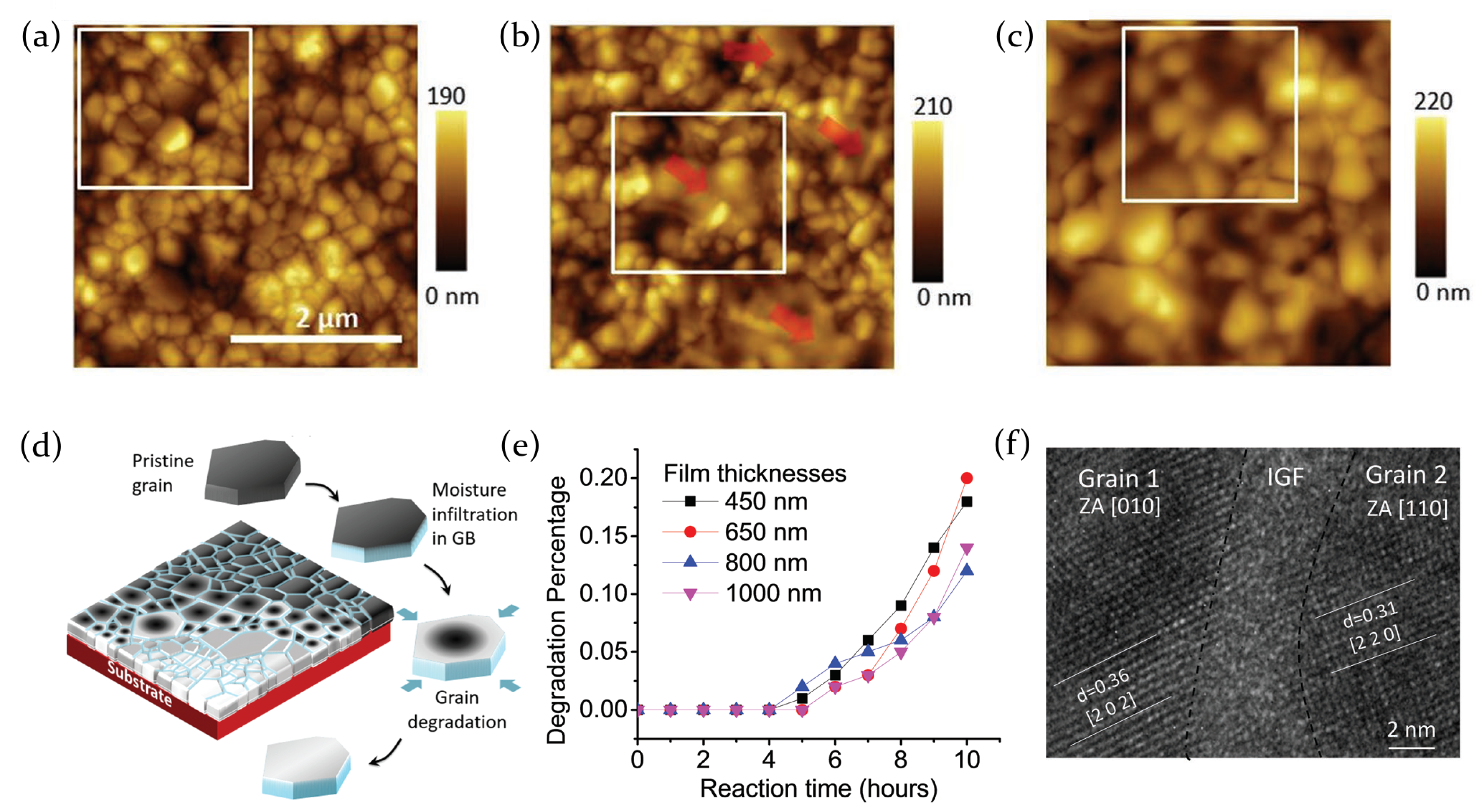
- Wang, Q.; Chen, B.; Liu, Y.; Deng, Y.; Bai, Y.; Dong, Q.; Huang, J. Scaling behavior of moisture-induced grain degradation in polycrystalline hybrid perovskite thin films. Energy Environ. Sci. 2017, 10, 516–522. [Google Scholar] [CrossRef]
- Yun, J.S.; Kim, J.; Young, T.; Patterson, R.J.; Kim, D.; Seidel, J.; Lim, S.; Green, M.A.; Huang, S.; Ho-Baillie, A. Humidity-Induced Degradation via Grain Boundaries of HC(NH 2)2PbI3 Planar Perovskite Solar Cells. Adv. Funct. Mater. 2018, 28, 1705363. [Google Scholar] [CrossRef]
- Howard, J.M.; Tennyson, E.M.; Barik, S.; Szostak, R.; Waks, E.; Toney, M.F.; Nogueira, A.F.; Neves, B.R.A.; Leite, M.S. Humidity-Induced Photoluminescence Hysteresis in Variable Cs/Br Ratio Hybrid Perovskites. J. Phys. Chem. Lett. 2018, 9, 3463–3469. [Google Scholar] [CrossRef]
- Fang, H.H.; Adjokatse, S.; Wei, H.; Yang, J.; Blake, G.R.; Huang, J.; Even, J.; Loi, M.A. Ultrahigh sensitivity of methylammonium lead tribromide perovskite single crystals to environmental gases. Sci. Adv. 2016, 2. [Google Scholar] [CrossRef]
- Zhang, H.; Liu, Y.; Lu, H.; Deng, W.; Yang, K.; Deng, Z.; Zhang, X.; Yuan, S.; Wang, J.; Niu, J.; et al. Reversible air-induced optical and electrical modulation of methylammonium lead bromide (MAPbBr3) single crystals. Appl. Phys. Lett. 2017, 111, 103904. [Google Scholar] [CrossRef]
- Tian, Y.; Peter, M.; Unger, E.; Abdellah, M.; Zheng, K.; Pullerits, T.; Yartsev, A.; Sundström, V.; Scheblykin, I.G. Mechanistic insights into perovskite photoluminescence enhancement: Light curing with oxygen can boost yield thousandfold. Phys. Chem. Chem. Phys. 2015, 17, 24978–24987. [Google Scholar] [CrossRef]
- Godding, J.S.; Ramadan, A.J.; Lin, Y.H.; Schutt, K.; Snaith, H.J.; Wenger, B. Oxidative Passivation of Metal Halide Perovskites. Joule 2019, 3, 2716–2731. [Google Scholar] [CrossRef]
- Brenes, R.; Guo, D.; Osherov, A.; Noel, N.; Eames, C.; Hutter, E.; Pathak, S.; Niroui, F.; Friend, R.; Islam, M.S.; et al. Metal Halide Perovskite Polycrystalline Films Exhibiting Properties of Single Crystals. Joule 2017, 1, 155–167. [Google Scholar] [CrossRef]
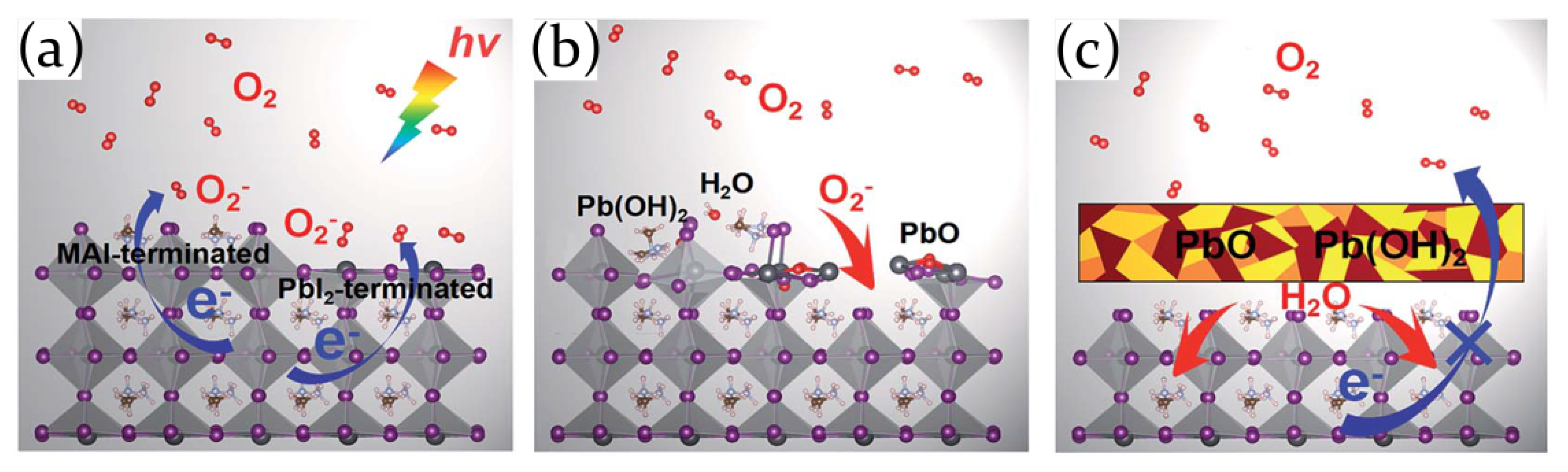
- Ouyang, Y.; Li, Y.; Zhu, P.; Li, Q.; Gao, Y.; Tong, J.; Shi, L.; Zhou, Q.; Ling, C.; Chen, Q.; et al. Photo-oxidative degradation of methylammonium lead iodide perovskite: Mechanism and protection. J. Mater. Chem. A 2019, 7, 2275–2282. [Google Scholar] [CrossRef]
- Anaya, M.; Galisteo-López, J.F.; Calvo, M.E.; Espinós, J.P.; Míguez, H. Origin of Light-Induced Photophysical Effects in Organic Metal Halide Perovskites in the Presence of Oxygen. J. Phys. Chem. Lett. 2018, 9, 3891–3896. [Google Scholar] [CrossRef]
- Aristidou, N.; Sanchez-Molina, I.; Chotchuangchutchaval, T.; Brown, M.; Martinez, L.; Rath, T.; Haque, S.A. The Role of Oxygen in the Degradation of Methylammonium Lead Trihalide Perovskite Photoactive Layers. Angew. Chem. Int. Ed. 2015, 54, 8208–8212. [Google Scholar] [CrossRef]
- Aristidou, N.; Eames, C.; Sanchez-Molina, I.; Bu, X.; Kosco, J.; Islam, M.S.; Haque, S.A. Fast oxygen diffusion and iodide defects mediate oxygen-induced degradation of perovskite solar cells. Nat. Commun. 2017, 8, 15218. [Google Scholar] [CrossRef]
- Lorenzon, M.; Sortino, L.; Akkerman, Q.; Accornero, S.; Pedrini, J.; Prato, M.; Pinchetti, V.; Meinardi, F.; Manna, L.; Brovelli, S. Role of Nonradiative Defects and Environmental Oxygen on Exciton Recombination Processes in CsPbBr3 Perovskite Nanocrystals. Nano Lett. 2017, 17, 3844–3853. [Google Scholar] [CrossRef]
- Maity, A.; Ghosh, B. Fast response paper based visual color change gas sensor for efficient ammonia detection at room temperature. Sci. Rep. 2018, 8. [Google Scholar] [CrossRef]
- Maity, A.; Raychaudhuri, A.; Ghosh, B. High sensitivity NH3 gas sensor with electrical readout made on paper with perovskite halide as sensor material. Sci. Rep. 2019, 9, 7777. [Google Scholar] [CrossRef]
- Singh, A.K.; Singh, S.; Singh, V.N.; Gupta, G.; Gupta, B.K. Probing reversible photoluminescence alteration in CH3NH3PbBr3 colloidal quantum dots for luminescence-based gas sensing application. J. Colloid Interface Sci. 2019, 554, 668–673. [Google Scholar] [CrossRef]
- Ruan, S.; Lu, J.; Pai, N.; Ebendorff-Heidepriem, H.; Cheng, Y.B.; Ruan, Y.; McNeill, C.R. An optical fibre-based sensor for the detection of gaseous ammonia with methylammonium lead halide perovskite. J. Mater. Chem. C 2018, 6, 6988–6995. [Google Scholar] [CrossRef]
- Bao, C.; Yang, J.; Zhu, W.; Zhou, X.; Gao, H.; Li, F.; Fu, G.; Yu, T.; Zou, Z. A resistance change effect in perovskite CH3NH3PbI3 films induced by ammonia. Chem. Commun. 2015, 51, 15426–15429. [Google Scholar] [CrossRef]
- Zhao, Y.; Zhu, K. Optical bleaching of perovskite (CH3NH3)PbI3 through room-temperature phase transformation induced by ammonia. Chem. Commun. 2014, 50, 1605–1607. [Google Scholar] [CrossRef] [PubMed]
- Huang, H.; Hao, M.; Song, Y.; Dang, S.; Liu, X.; Dong, Q. Dynamic Passivation in Perovskite Quantum Dots for Specific Ammonia Detection at Room Temperature. Small 2020, 16, 1904462. [Google Scholar] [CrossRef]
- Fu, X.; Jiao, S.; Dong, N.; Lian, G.; Zhao, T.; Lv, S.; Wang, Q.; Cui, D. A CH3NH3PbI3 film for a room-temperature NO2 gas sensor with quick response and high selectivity. RSC Adv. 2018, 8, 390–395. [Google Scholar] [CrossRef]
- Zhang, Z.J.; Xiang, S.C.; Guo, G.C.; Xu, G.; Wang, M.S.; Zou, J.P.; Guo, S.P.; Huang, J.S. Wavelength-Dependent Photochromic Inorganic–Organic Hybrid Based on a 3D Iodoplumbate Open-Framework Material. Angew. Chem. Int. Ed. 2008, 47, 4149–4152. [Google Scholar] [CrossRef]
- Huang, H.; Xu, Y.; Feng, Q.; Leung, D.Y.C. Low temperature catalytic oxidation of volatile organic compounds: A review. Catal. Sci. Technol. 2015, 5, 2649–2669. [Google Scholar] [CrossRef]
- Shuai, J.; Kim, S.; Ryu, H.; Park, J.; Lee, C.; Kim, G.B.; Ultra, V.U., Jr.; Yang, W. Health risk assessment of volatile organic compounds exposure near Daegu dyeing industrial complex in South Korea. BMC Public Health 2018, 18. [Google Scholar] [CrossRef]
- Hempel-Jorgensen, A.; Kjaergaard, S.K.; Molhave, L.; Hudnell, K.H. Sensory Eye Irritation in Humans Exposed to Mixtures of Volatile Organic Compounds. Arch. Environ. Health 1999, 54, 416–424. [Google Scholar] [CrossRef]
- Ahn, K. The role of air pollutants in atopic dermatitis. J. Allergy Clin. Immunol. 2014, 5, 993–1000. [Google Scholar] [CrossRef]
- Otto, D.A.; Hudnell, H.K.; House, D.E.; Mølhave, L.; Counts, W. Exposure of Humans to a Volatile Organic Mixture. I. Behavioral Assessment. Arch. Environ. Health 1992, 47, 23–30. [Google Scholar] [CrossRef] [PubMed]
- Genc, S.; Zadeoglulari, Z.; Fuss, S.; Genc, K. The Adverse Effects of Air Pollution on the Nervous System. J. Toxicol. 2012, 2012, 782462. [Google Scholar] [CrossRef] [PubMed]
- Wei, L.Y.; Ma, W.; Lian, C.; Meng, S. Benign Interfacial Iodine Vacancies in Perovskite Solar Cells. J. Phys. Chem. C 2017, 121, 5905–5913. [Google Scholar] [CrossRef]
- Kim, S.H.; Kirakosyan, A.; Choi, J.; Kim, J.H. Detection of volatile organic compounds (VOCs), aliphatic amines, using highly fluorescent organic-inorganic hybrid perovskite nanoparticles. Dyes Pigm. 2017, 147, 1–5. [Google Scholar] [CrossRef]
- Giorgi, G.; Fujisawa, J.I.; Segawa, H.; Yamashita, K. Cation Role in Structural and Electronic Properties of 3D Organic-Inorganic Halide Perovskites: A DFT Analysis. J. Phys. Chem. C 2014, 118, 12176–12183. [Google Scholar] [CrossRef]
- Kakavelakis, G.; Gagaoudakis, E.; Petridis, K.; Petromichelaki, V.; Binas, V.; Kiriakidis, G.; Kymakis, E. Solution Processed CH3NH3PbI3−xClx Perovskite Based Self-Powered Ozone Sensing Element Operated at Room Temperature. ACS Sens. 2018, 3, 135–142. [Google Scholar] [CrossRef]
- Wen, X.; Wu, J.; Gao, D.; Lin, C. Interfacial engineering with amino-functionalized graphene for efficient perovskite solar cells. J. Mater. Chem. A 2016, 4, 13482–13487. [Google Scholar] [CrossRef]
- Department of Health and Human Services. US Food and Drug Administration, Federal Register. 1997. Available online: https://www.govinfo.gov/content/pkg/FR-1997-04-17/pdf/97-9706.pdf (accessed on 15 December 2020).
- Acharyya, D.; Bhattacharyya, P. Alcohol sensing performance of ZnO hexagonal nanotubes at low temperatures: A qualitative understanding. Sens. Actuators B 2016, 228, 373–386. [Google Scholar] [CrossRef]
- Liang, J.; Wang, C.; Wang, Y.; Xu, Z.; Lu, Z.; Ma, Y.; Zhu, H.; Hu, Y.; Xiao, C.; Yi, X.; et al. All-Inorganic Perovskite Solar Cells. J. Am. Chem. Soc. 2016, 138, 15829–15832. [Google Scholar] [CrossRef]
- Beal, R.E.; Slotcavage, D.J.; Leijtens, T.; Bowring, A.R.; Belisle, R.A.; Nguyen, W.H.; Burkhard, G.F.; Hoke, E.T.; McGehee, M.D. Cesium Lead Halide Perovskites with Improved Stability for Tandem Solar Cells. J. Phys. Chem. Lett. 2016, 7, 746–751. [Google Scholar] [CrossRef]
- Chen, H.; Zhang, M.; Bo, R.; Barugkin, C.; Zheng, J.; Ma, Q.; Huang, S.; Ho-Baillie, A.W.Y.; Catchpole, K.R.; Tricoli, A. Superior Self-Powered Room-Temperature Chemical Sensing with Light-Activated Inorganic Halides Perovskites. Small 2018, 14, 1702571. [Google Scholar] [CrossRef] [PubMed]
- Muthu, C.; Nagamma, S.R.; Nair, V.C. Luminescent hybrid perovskite nanoparticles as a new platform for selective detection of 2,4,6-trinitrophenol. RSC Adv. 2014, 4, 55908–55911. [Google Scholar] [CrossRef]
- Wang, Y.; Ren, Y.; Zhang, S.; Wu, J.; Song, J.; Li, X.; Jiayue, X.; Sow, C.; Zeng, H.; Sun, H. Switching excitonic recombination and carrier trapping in cesium lead halide perovskites by air. Commun. Phys. 2018, 1. [Google Scholar] [CrossRef]
- Lu, D.; Zhang, Y.; Lai, M.; Lee, A.; Xie, C.; Lin, J.; Lei, T.; Lin, Z.; Kley, C.S.; Huang, J.; et al. Giant Light-Emission Enhancement in Lead Halide Perovskites by Surface Oxygen Passivation. Nano Lett. 2018, 18, 6967–6973. [Google Scholar] [CrossRef]
- Harwell, J.R.; Glackin, J.M.E.; Davis, N.J.L.K.; Gillanders, R.N.; Credgington, D.; Turnbull, G.A.; Samuel, I.D.W. Sensing of explosive vapor by hybrid perovskites: Effect of dimensionality. APL Mater. 2020, 8, 071106. [Google Scholar] [CrossRef]
- Li, J.; Si, J.; Gan, L.; Liu, Y.; Ye, Z.; He, H. Simple Approach to Improving the Amplified Spontaneous Emission Properties of Perovskite Films. ACS Appl. Mater. Interfaces 2016, 8, 32978–32983. [Google Scholar] [CrossRef]
- Qin, L.; Lv, L.; Li, C.; Zhu, L.; Cui, Q.; Hu, Y.; Lou, Z.; Teng, F.; Hou, Y. Temperature dependent amplified spontaneous emission of vacuum annealed perovskite films. RSC Adv. 2017, 7, 15911–15916. [Google Scholar] [CrossRef]
- Balena, A.; Perulli, A.; Fernandez, M.; De Giorgi, M.L.; Nedelcu, G.; Kovalenko, M.V.; Anni, M. Temperature Dependence of the Amplified Spontaneous Emission from CsPbBr3 Nanocrystal Thin Films. J. Phys. Chem. C 2018, 122, 5813–5819. [Google Scholar] [CrossRef]
- Papagiorgis, P.; Manoli, A.; Protesescu, L.; Achilleos, C.; Violaris, M.; Nicolaides, K.; Trypiniotis, T.; Bodnarchuk, M.I.; Kovalenko, M.V.; Othonos, A.; et al. Efficient Optical Amplification in the Nanosecond Regime from Formamidinium Lead Iodide Nanocrystals. ACS Photonics 2018, 5, 907–917. [Google Scholar] [CrossRef]
- Veldhuis, S.A.; Tay, Y.K.E.; Bruno, A.; Dintakurti, S.S.H.; Bhaumik, S.; Muduli, S.K.; Li, M.; Mathews, N.; Sum, T.C.; Mhaisalkar, S.G. Benzyl Alcohol-Treated CH3NH3PbBr3 Nanocrystals Exhibiting High Luminescence, Stability, and Ultralow Amplified Spontaneous Emission Thresholds. Nano Lett. 2017, 17, 7424–7432. [Google Scholar] [CrossRef]
- Dey, A.; Rathod, P.; Kabra, D. Role of Localized States in Photoluminescence Dynamics of High Optical Gain CsPbBr3 Nanocrystals. Adv. Opt. Mater. 2018, 6, 1800109. [Google Scholar] [CrossRef]
- Rose, A.; Zhu, Z.; Madigan, C.F.; Swager, T.M.; Bulovic, V. Sensitivity gains in chemosensing by lasing action in organic polymers. Nature 2005, 434, 876–879. [Google Scholar] [CrossRef] [PubMed]
- Lin, H.W.; Huang, M.H.; Chen, Y.H.; Lin, W.C.; Cheng, H.C.; Wu, C.C.; Chao, T.C.; Wang, T.C.; Wong, K.T.; Tang, K.C.; et al. Novel oxygen sensor based on terfluorene thin-film and its enhanced sensitivity by stimulated emission. J. Mater. Chem. 2012, 22, 13446–13450. [Google Scholar] [CrossRef]


| Perovskite | Structure | Target Gas | Sensitivity | LOD | Ref. | |||
|---|---|---|---|---|---|---|---|---|
| Polycrystalline | 0.4 s | 3000 | [66] | |||||
| Thin film | 3 s | 4.5 s | [84] | |||||
| Nanorods | ≃130 s | ≃120 s | ≃90% | 1 ppm | [81] | |||
| Thin film | 5 s | 25 s | 0.62 ppm | 1 ppm | [87] | |||
| Thin film | 3.7 min | 6 min | 200 ppb | [49] | ||||
| Acetone | 4.5 min | 4 min | 20 ppm | |||||
| Thin film | Ethanol | 66 s | 67 s | 1300 ppm | [7] | |||
| Thin film | 188 s | 40 s | 9.69 | 5 ppb | [98] | |||
| Thin film | 39 s | 61 s | 0.3% | 10 ppm | [8] | |||
| Single crystal | Air | [71] | ||||||
| Nanocrystals | 17 s | 128 s | 0.93 | 10,000 ppm | [104] | |||
| Acetone | 9.8 s | 5.8 s | 0.03 | 1 ppm | ||||
| Ethanol | 0.025 | 1 ppm |
Publisher’s Note: MDPI stays neutral with regard to jurisdictional claims in published maps and institutional affiliations. |
© 2021 by the authors. Licensee MDPI, Basel, Switzerland. This article is an open access article distributed under the terms and conditions of the Creative Commons Attribution (CC BY) license (http://creativecommons.org/licenses/by/4.0/).
Share and Cite
De Giorgi, M.L.; Milanese, S.; Klini, A.; Anni, M. Environment-Induced Reversible Modulation of Optical and Electronic Properties of Lead Halide Perovskites and Possible Applications to Sensor Development: A Review. Molecules 2021, 26, 705. https://doi.org/10.3390/molecules26030705
De Giorgi ML, Milanese S, Klini A, Anni M. Environment-Induced Reversible Modulation of Optical and Electronic Properties of Lead Halide Perovskites and Possible Applications to Sensor Development: A Review. Molecules. 2021; 26(3):705. https://doi.org/10.3390/molecules26030705
Chicago/Turabian StyleDe Giorgi, Maria Luisa, Stefania Milanese, Argyro Klini, and Marco Anni. 2021. "Environment-Induced Reversible Modulation of Optical and Electronic Properties of Lead Halide Perovskites and Possible Applications to Sensor Development: A Review" Molecules 26, no. 3: 705. https://doi.org/10.3390/molecules26030705
APA StyleDe Giorgi, M. L., Milanese, S., Klini, A., & Anni, M. (2021). Environment-Induced Reversible Modulation of Optical and Electronic Properties of Lead Halide Perovskites and Possible Applications to Sensor Development: A Review. Molecules, 26(3), 705. https://doi.org/10.3390/molecules26030705