
Fabrication of Eutectic Ga-In Nanowire Arrays Based on Plateau–Rayleigh Instability


Abstract
:1. Introduction
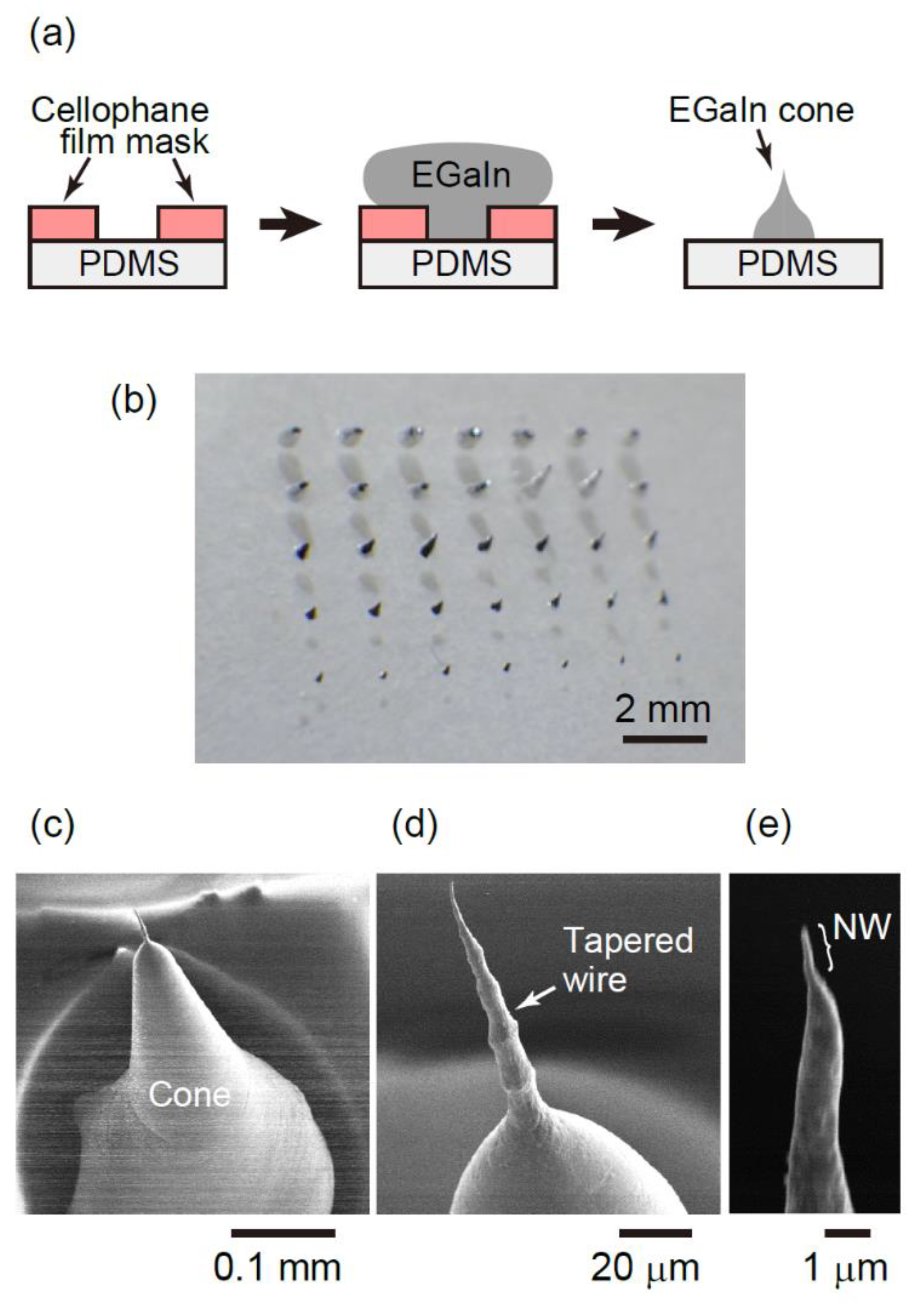
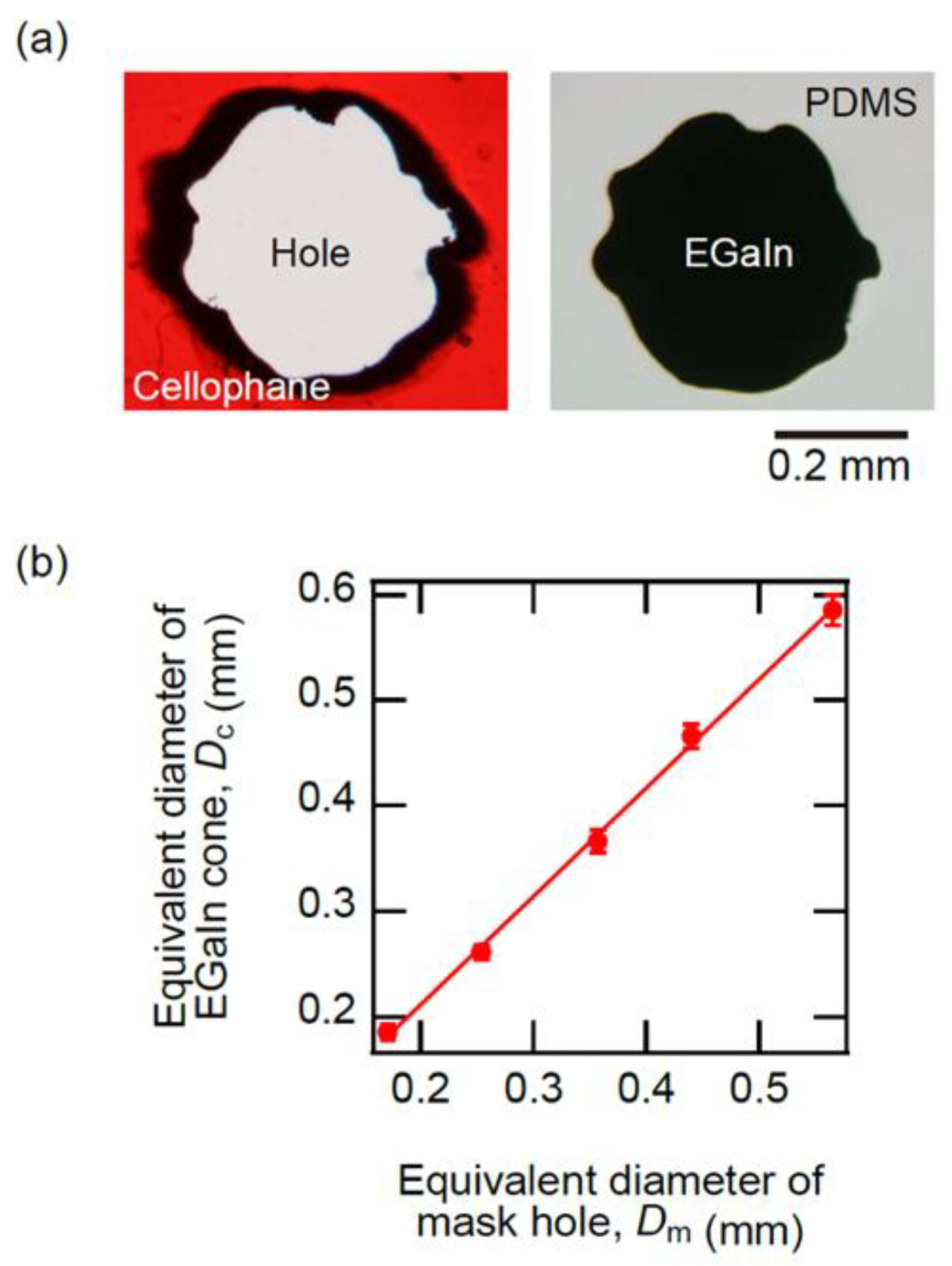
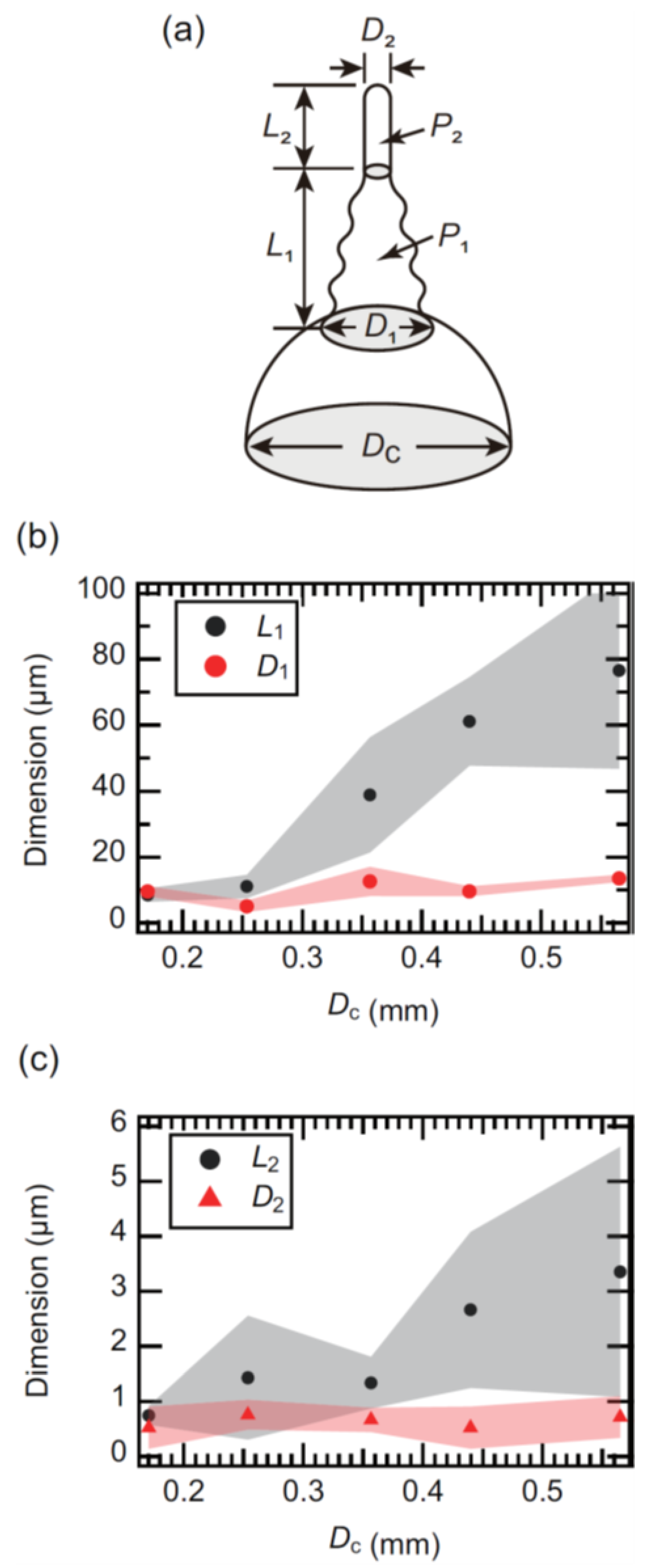
2. Experimental
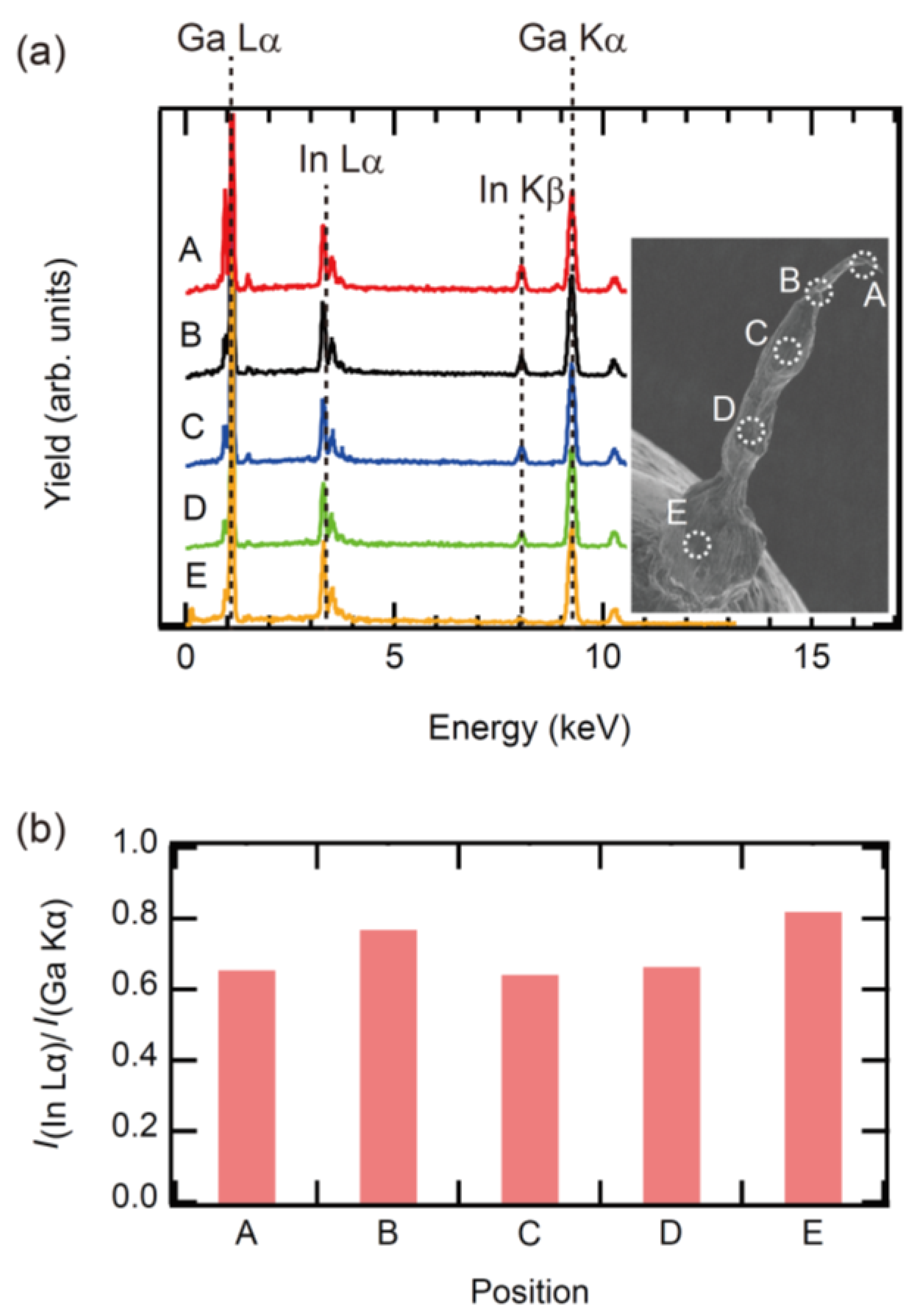
3. Results and Discussion
Author Contributions
Funding
Institutional Review Board Statement
Informed Consent Statement
Data Availability Statement
Acknowledgments
Conflicts of Interest
Sample Availability
References
- Daeneke, T.; Khoshmanesh, K.; Mahmood, N.; de Castro, I.A.; Esrafilzadeh, D.; Barrow, S.J.; Dickey, M.D.; Kalantar-Zadeh, K. Liquid metals: Fundamentals and applications in chemistry. Chem. Soc. Rev. 2018, 47, 4073–4111. [Google Scholar] [CrossRef] [PubMed]
- Bo, G.; Ren, L.; Xu, X.; Du, Y.; Dou, S. Recent progress on liquid metals and their applications. Adv. Phys. X 2018, 3, 1446359. [Google Scholar] [CrossRef] [Green Version]
- Matsukawa, R.; Kobayashi, D.; Mitsui, H.; Ikuno, T. Environment-friendly paper-based flexible pressure sensors with carbon nanotubes and liquid metal. Appl. Phys. Express 2020, 13, 027001. [Google Scholar] [CrossRef]
- Boley, J.W.; White, E.L.; Kramer, R.K. Mechanically sintered gallium-indium nanoparticles. Adv. Mater. 2015, 27, 2355–2360. [Google Scholar] [CrossRef]
- Zhang, B.; Dong, Q.; Korman, C.E.; Li, Z.; Zaghloul, M.E. Flexible packaging of solid-state integrated circuit chips with elastomeric microfluidics. Sci. Rep. 2013, 3. [Google Scholar] [CrossRef] [Green Version]
- Guo, R.; Wang, X.; Chang, H.; Yu, W.; Liang, S.; Rao, W.; Liu, J. Ni-GaIn Amalgams Enabled Rapid and Customizable Fabrication of Wearable and Wireless Healthcare Electronics. Adv. Eng. Mater. 2018, 20, 1–8. [Google Scholar] [CrossRef]
- Michaud, H.O.; Teixidor, J.; Lacour, S.P. Soft metal constructs for large strain sensor membrane. Smart Mater. Struct. 2015, 24, 035020. [Google Scholar] [CrossRef] [Green Version]
- Yong-Lae, P.; Bor-Rong, C.; Wood, R.J. Design and Fabrication of Soft Artificial Skin Using Embedded Microchannels and Liquid Conductors. IEEE Sens. J. 2012, 12, 2711–2718. [Google Scholar] [CrossRef]
- Jackson, N.; Buckley, J.; Clarke, C.; Stam, F. Manufacturing methods of stretchable liquid metal-based antenna. Microsyst. Technol. 2018, 25, 3175–3184. [Google Scholar] [CrossRef]
- Jin, C.; Zhang, J.; Li, X.; Yang, X.; Li, J.; Liu, J. Injectable 3-D fabrication of medical electronics at the target biological tissues. Sci. Rep. 2013, 3, 3442. [Google Scholar] [CrossRef] [PubMed] [Green Version]
- Kim, S.; Oh, J.; Jeong, D.; Bae, J. Direct Wiring of Eutectic Gallium-Indium to a Metal Electrode for Soft Sensor Systems. ACS Appl. Mater. Interfaces 2019, 11, 20557–20565. [Google Scholar] [CrossRef]
- Kim, T.; Kim, D.M.; Lee, B.J.; Lee, J. Soft and Deformable Sensors Based on Liquid Metals. Sensors 2019, 19, 4250. [Google Scholar] [CrossRef] [PubMed] [Green Version]
- Li, Q.; Lin, J.; Liu, T.; Zheng, H.; Liu, J. Printed flexible thin-film transistors based on different types of modified liquid metal with good mobility. Sci. China Inf. Sci. 2019, 62, 1–12. [Google Scholar] [CrossRef] [Green Version]
- Varga, M.; Ladd, C.; Ma, S.; Holbery, J.; Troster, G. On-skin liquid metal inertial sensor. Lab Chip 2017, 17, 3272–3278. [Google Scholar] [CrossRef]
- Yu, Y.; Zhang, J.; Liu, J. Biomedical implementation of liquid metal ink as drawable ECG electrode and skin circuit. PLoS ONE 2013, 8, e058771. [Google Scholar] [CrossRef]
- Ikuno, T.; Katayama, M.; Kishida, M.; Kamada, K.; Murata, Y.; Yasuda, T.; Honda, S.; Lee, J.G.; Mori, H.; Oura, K. Metal-coated carbon nanotube tip for scanning tunneling microscope. Jpn. J. Appl. Phys. 2004, 43, L644–L646. [Google Scholar] [CrossRef]
- Ikuno, T.; Yasuda, T.; Honda, S.I.; Oura, K.; Katayama, M.; Lee, J.G.; Mori, H. Coating carbon nanotubes with inorganic materials by pulsed laser deposition. J. Appl. Phys. 2005, 98, 114305. [Google Scholar] [CrossRef]
- Murata, X.; Yoshimoto, S.; Kishida, M.; Maeda, D.; Yasuda, T.; Ikuno, T.; Honda, S.; Okado, H.; Hobara, R.; Matsuda, I.; et al. Exploiting metal coating of carbon nanotubes for scanning tunneling microscopy probes. Jpn. J. Appl. Phys. 2005, 44, 5336–5338. [Google Scholar] [CrossRef]
- Ławrowski, R.; Pirker, L.; Kaneko, K.; Kokubo, H.; Bachmann, M.; Ikuno, T.; Remskar, M.; Schreiner, R. Field emission from nanotubes and flakes of transition metal dichalcogenides. J. Vac. Sci. Technol. B 2020, 38, 032801. [Google Scholar] [CrossRef]
- Ladd, C.; So, J.H.; Muth, J.; Dickey, M.D. 3D printing of free standing liquid metal microstructures. Adv. Mater. 2013, 25, 5081–5085. [Google Scholar] [CrossRef] [PubMed]
- Eggers, J. Nonlinear dynamics and breakup of free-surface flows. Rev. Mod. Phys. 1997, 69, 865–930. [Google Scholar] [CrossRef] [Green Version]
- Papageorgiou, D.T. On the breakup of viscous liquid threads. Phys. Fluids 1995, 7, 1529–1544. [Google Scholar] [CrossRef] [Green Version]
- Ojaghlou, N.; Tafreshi, H.V.; Bratko, D.; Luzar, A. Dynamical insights into the mechanism of a droplet detachment from a fiber. Soft Matter. 2018, 14, 8924–8934. [Google Scholar] [CrossRef]
- Anna, S.L.; McKinley, G.H. Elasto-capillary thinning and breakup of model elastic liquids. J. Rheol. 2001, 45, 115–138. [Google Scholar] [CrossRef] [Green Version]
- Chen, H.; Ponce-Torres, A.; Montanero, J.M.; Amirfazli, A. Viscoelastic liquid bridge breakup and liquid transfer between two surfaces. J. Colloid. Interface Sci. 2021, 582, 1251–1256. [Google Scholar] [CrossRef] [PubMed]
- Dinic, J.; Sharma, V. Power Laws Dominate Shear and Extensional Rheology Response and Capillarity-Driven Pinching Dynamics of Entangled Hydroxyethyl Cellulose (HEC) Solutions. Macromolecules 2020, 53, 3424–3437. [Google Scholar] [CrossRef]
- Chiechi, R.C.; Weiss, E.A.; Dickey, M.D.; Whitesides, G.M. Eutectic gallium-indium (EGaIn): A moldable liquid metal for electrical characterization of self-assembled monolayers. Angew. Chem. Int. Ed. Engl. 2008, 47, 142–144. [Google Scholar] [CrossRef] [PubMed]
- Li, J.; Fontelos, M.A. Drop dynamics on the beads-on-string structure for viscoelastic jets: A numerical study. Phys. Fluids 2003, 15, 922–937. [Google Scholar] [CrossRef]
- Montanero, J.M.; Ponce-Torres, A. Review on the Dynamics of Isothermal Liquid Bridges. Appl. Mech. Rev. 2020, 72, 010803. [Google Scholar] [CrossRef]
- Anderson, T.J.; Ansara, I. The Ga-In (Gallium-Indium) System. J. Phase Equilibria Diffus. 1991, 12, 64. [Google Scholar] [CrossRef]
Publisher’s Note: MDPI stays neutral with regard to jurisdictional claims in published maps and institutional affiliations. |
© 2021 by the authors. Licensee MDPI, Basel, Switzerland. This article is an open access article distributed under the terms and conditions of the Creative Commons Attribution (CC BY) license (https://creativecommons.org/licenses/by/4.0/).
Share and Cite
Ikuno, T.; Somei, Z. Fabrication of Eutectic Ga-In Nanowire Arrays Based on Plateau–Rayleigh Instability. Molecules 2021, 26, 4616. https://doi.org/10.3390/molecules26154616
Ikuno T, Somei Z. Fabrication of Eutectic Ga-In Nanowire Arrays Based on Plateau–Rayleigh Instability. Molecules. 2021; 26(15):4616. https://doi.org/10.3390/molecules26154616
Chicago/Turabian StyleIkuno, Takashi, and Zen Somei. 2021. "Fabrication of Eutectic Ga-In Nanowire Arrays Based on Plateau–Rayleigh Instability" Molecules 26, no. 15: 4616. https://doi.org/10.3390/molecules26154616
APA StyleIkuno, T., & Somei, Z. (2021). Fabrication of Eutectic Ga-In Nanowire Arrays Based on Plateau–Rayleigh Instability. Molecules, 26(15), 4616. https://doi.org/10.3390/molecules26154616