
Seeding, Plating and Electrical Characterization of Gold Nanowires Formed on Self-Assembled DNA Nanotubes

 , and
, and
Abstract
1. Introduction
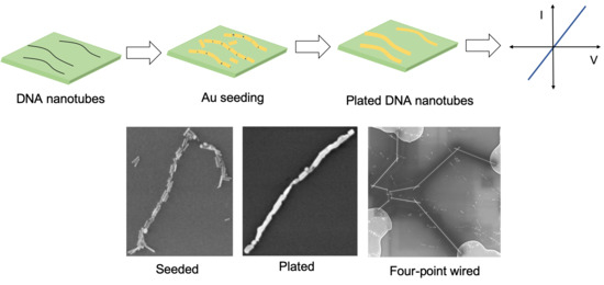
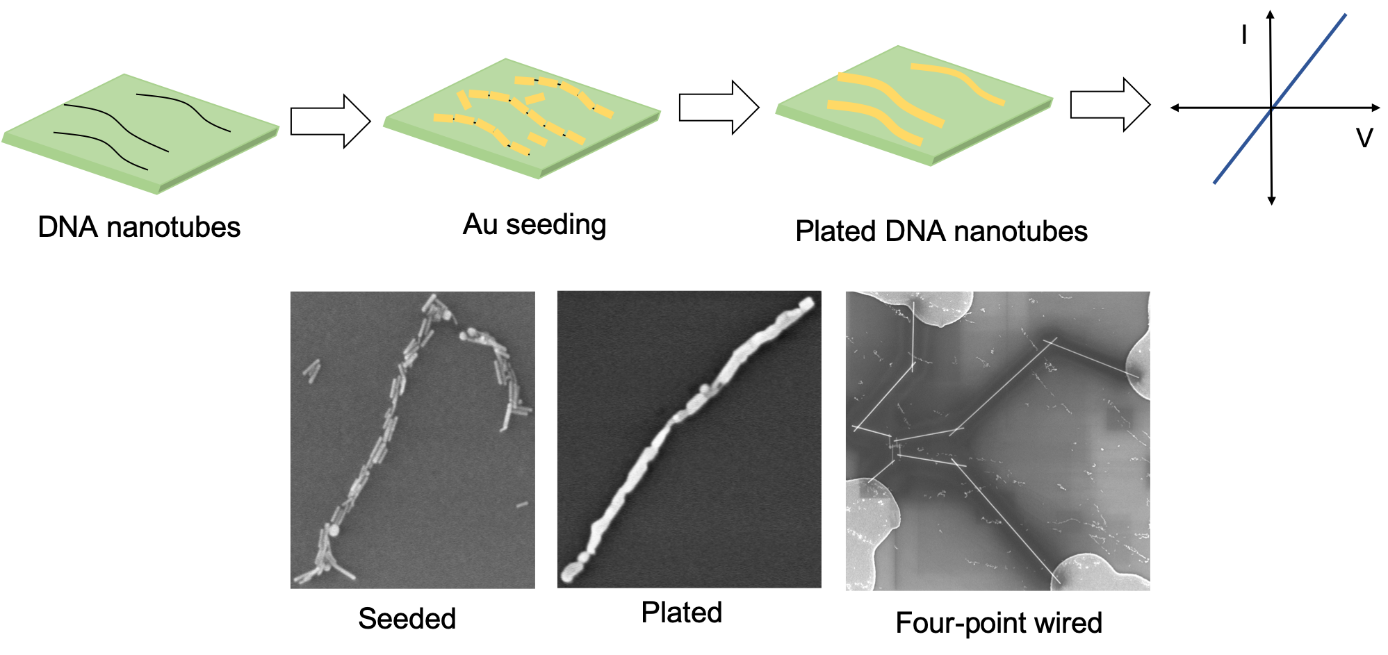
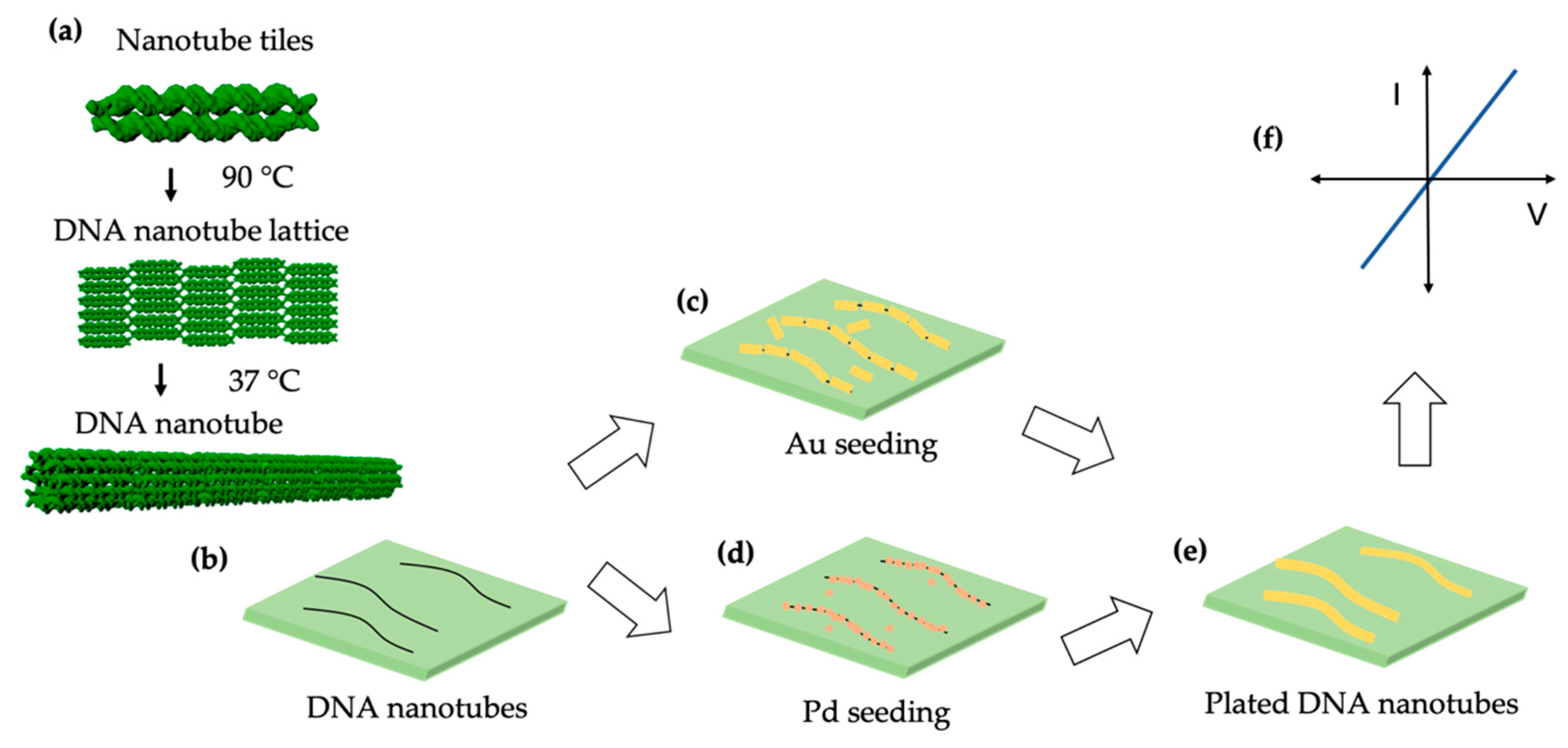
2. Results
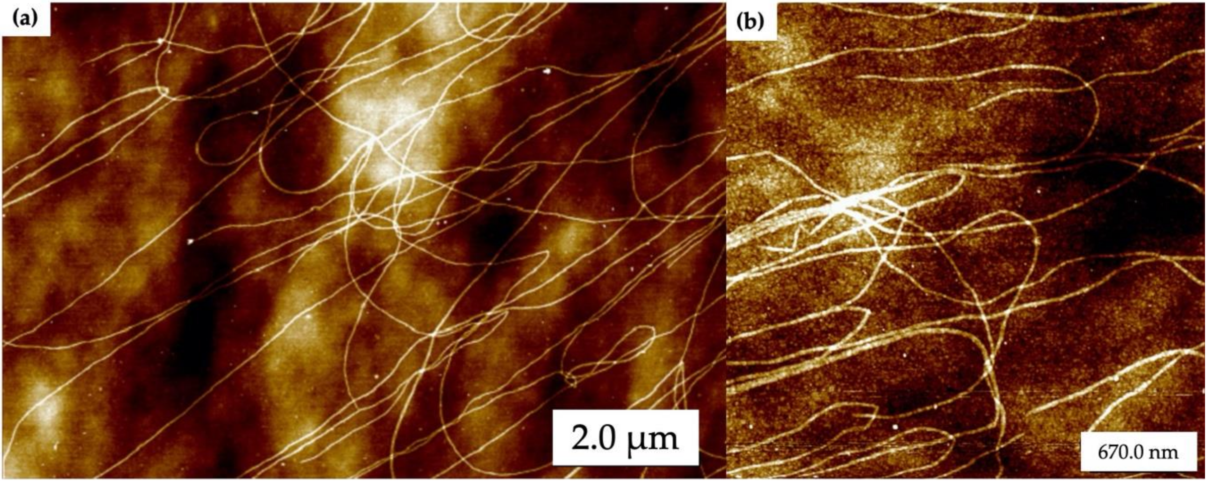
2.1. Deposition of DNA Nanotubes
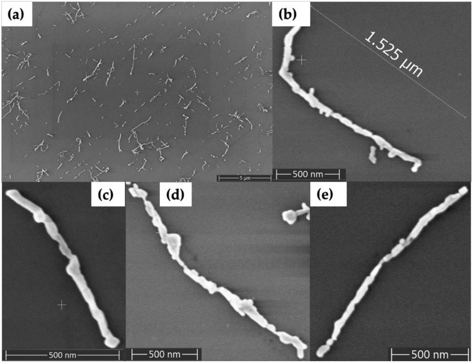
2.2. Au Nanorod Seeding of DNA Nanotubes
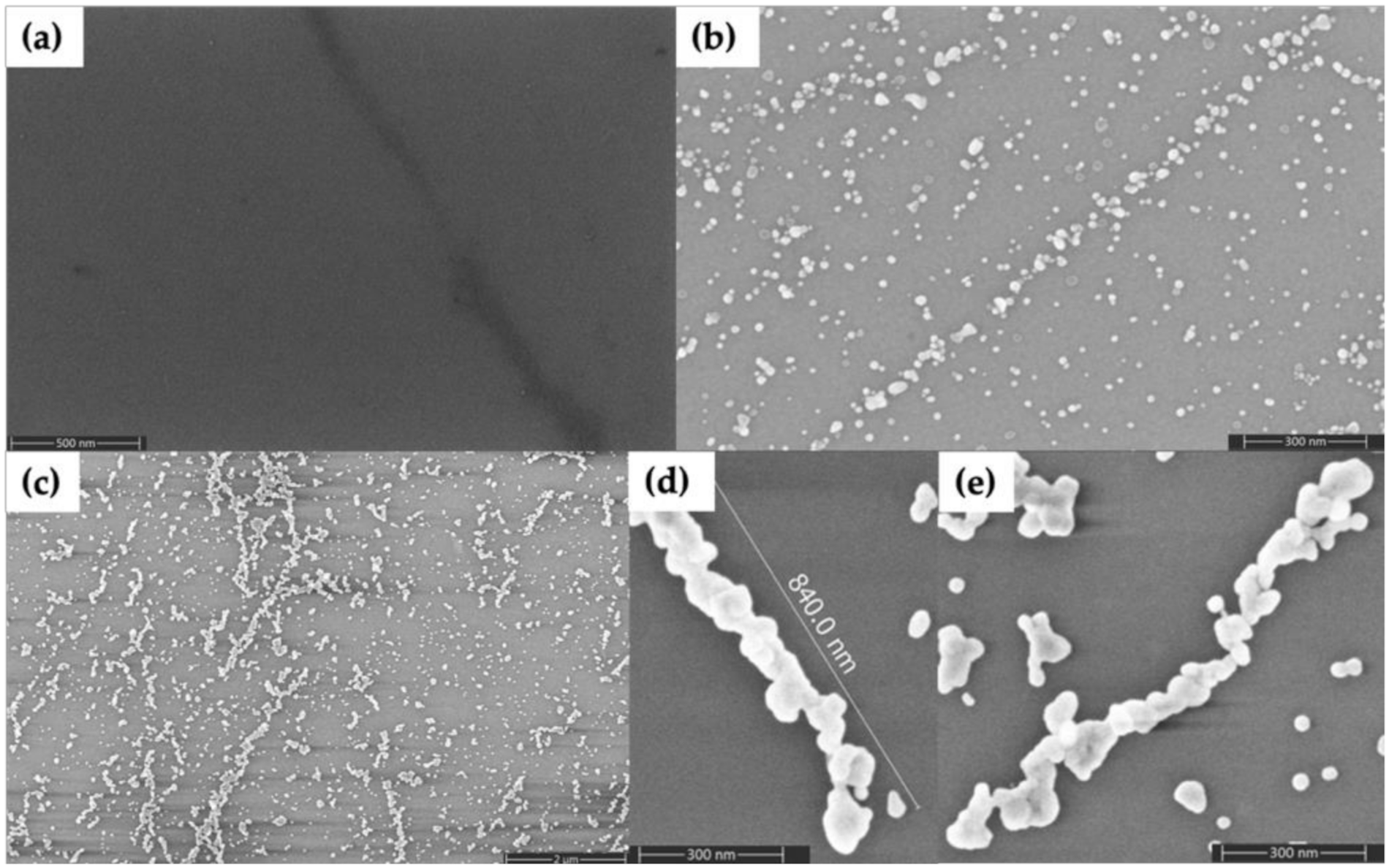
2.3. Au Nanorod-Seeded and Au-Plated DNA Nanotubes
2.4. Pd-Seeded and Au-Plated DNA Nanotubes
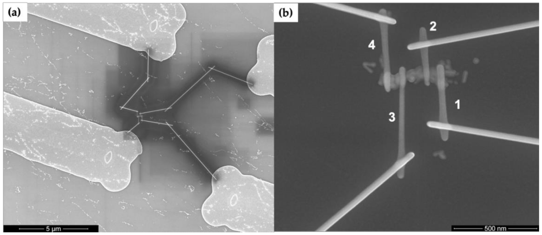
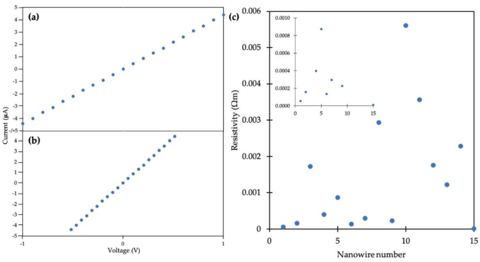
2.5. Electrical Characterization
3. Discussion
4. Materials and Methods
4.1. Chemicals and Materials
4.2. Sample Preparation
4.2.1. DNA Nanotube Deposition
4.2.2. Seeding Au Nanorods on DNA Nanotubes
4.2.3. Pd Seeding on DNA Nanotubes
4.2.4. Plating Au on Seeded DNA Nanotubes
4.2.5. EBID and Creating Electrical Connections
4.3. Characterization
4.3.1. AFM Imaging
4.3.2. SEM Imaging
4.3.3. Electrical Measurements
5. Conclusions
Supplementary Materials
Author Contributions
Funding
Acknowledgments
Conflicts of Interest
References
- Peng, Z.; Liu, H. Bottom-up Nanofabrication Using DNA Nanostructures. Chem. Mater. 2016, 28, 1012–1021. [Google Scholar] [CrossRef]
- Liddle, J.A.; Gallatin, G.M. Nanomanufacturing: A Perspective. ACS Nano 2016, 10, 2995–3014. [Google Scholar] [CrossRef] [PubMed]
- Biswas, A.; Bayer, I.S.; Biris, A.S.; Wang, T.; Dervishi, E.; Faupel, F. Advances in top–down and bottom–up surface nanofabrication: Techniques, applications & future prospects. Adv. Colloid Interface Sci. 2012, 170, 2–27. [Google Scholar] [CrossRef] [PubMed]
- Mijatovic, D.; Eijkel, J.C.T.; van den Berg, A. Technologies for nanofluidic systems: Top-down vs. bottom-up—A review. Lab. Chip 2005, 5, 492–500. [Google Scholar] [CrossRef]
- Thiruvengadathan, R.; Korampally, V.; Ghosh, A.; Chanda, N.; Gangopadhyay, K.; Gangopadhyay, S. Nanomaterial processing using self-assembly-bottom-up chemical and biological approaches. Rep. Prog. Phys. 2013, 76, 066501. [Google Scholar] [CrossRef]
- Kumar, S.; Bhushan, P.; Bhattacharya, S. Fabrication of Nanostructures with Bottom-up Approach and Their Utility in Diagnostics, Therapeutics, and Others. In Environmental, Chemical and Medical Sensor; Bhattacharya, S., Agarwal, A.K., Chanda, N., Pandey, A., Sen, A.K., Eds.; Springer: Singapore, 2018; pp. 167–198. [Google Scholar] [CrossRef]
- Ma, R.-I.; Kallenbach, N.R.; Sheardy, R.D.; Petrillo, M.L.; Seeman, N.C. Three-arm nucleic acid junctions are flexible. Nucleic Acids Res. 1986, 14, 9745–9753. [Google Scholar] [CrossRef]
- Rothemund, P.W.K. Folding DNA to create nanoscale shapes and patterns. Nature 2006, 440, 297–302. [Google Scholar] [CrossRef]
- Liu, X.; Zhao, Y.; Liu, P.; Wang, L.; Lin, J.; Fan, C. Biomimetic DNA Nanotubes: Nanoscale Channel Design and Applications. Angew. Chem. Int. 2019, 58, 8996–9011. [Google Scholar] [CrossRef]
- Bui, H.; Onodera, C.; Kidwell, C.; Tan, Y.; Graugnard, E.; Kuang, W.; Lee, J.; Knowlton, W.B.; Yurke, B.; Hughes, W.L. Programmable Periodicity of Quantum Dot Arrays with DNA Origami Nanotubes. Nano Lett. 2010, 10, 3367–3372. [Google Scholar] [CrossRef]
- Ge, J.; Zhao, Y.; Li, C.; Jie, G. Versatile Electrochemiluminescence and Electrochemical “On–Off” Assays of Methyltransferases and Aflatoxin B1 Based on a Novel Multifunctional DNA Nanotube. Anal. Chem. 2019, 91, 3546–3554. [Google Scholar] [CrossRef]
- Rothemund, P.W.K.; Ekani-Nkodo, A.; Papadakis, N.; Kumar, A.; Fygenson, D.K.; Winfree, E. Design and Characterization of Programmable DNA Nanotubes. J. Am. Chem. Soc. 2004, 126, 16344–16352. [Google Scholar] [CrossRef] [PubMed]
- Park, S.H.; Yan, H.; Reif, J.H.; LaBean, T.H.; Finkelstein, G. Electronic nanostructures templated on self-assembled DNA scaffolds. Nanotechnology 2004, 15, S525–S527. [Google Scholar] [CrossRef]
- Lo, P.K.; Karam, P.; Aldaye, F.A.; McLaughlin, C.K.; Hamblin, G.D.; Cosa, G.; Sleiman, H.F. Loading and selective release of cargo in DNA nanotubes with longitudinal variation. Nat. Chem. 2010, 2, 319–328. [Google Scholar] [CrossRef] [PubMed]
- Gopinath, A.; Rothemund, P.W.K. Optimized Assembly and Covalent Coupling of Single-Molecule DNA Origami Nanoarrays. ACS Nano 2014, 8, 12030–12040. [Google Scholar] [CrossRef]
- Shetty, R.M.; Brady, S.R.; Rothemund, P.W.K.; Hariadi, R.F.; Gopinath, A. Low-cost, bottom-up fabrication of large-scale single-molecule nanoarrays by DNA origami placement. bioRxiv 2020. [Google Scholar] [CrossRef]
- Gopinath, A.; Thachuk, C.; Mitskovets, A.; Atwater, H.A.; Kirkpatrick, D.; Rothemund, P.W.K. Absolute and arbitrary orientation of single molecule shapes. arXiv 2018, arXiv:1808.04544. [Google Scholar]
- Mohammed, A.M.; Schulman, R. Directing Self-Assembly of DNA Nanotubes Using Programmable Seeds. Nano Lett. 2013, 13, 4006–4013. [Google Scholar] [CrossRef]
- Mohammed, A.M.; Šulc, P.; Zenk, J.; Schulman, R. Self-assembling DNA nanotubes to connect molecular landmarks. Nat. Nanotechnol. 2017, 12, 312–316. [Google Scholar] [CrossRef]
- Lu, W.; Lieber, C.M. Nanoelectronics from the bottom up. Nat. Mater. 2007, 6, 841–850. [Google Scholar] [CrossRef]
- Porath, D.; Lapidot, N.; Gomez-Herrero, J. Charge Transport in DNA-based Devices. In Introducing Molecular Electronics; Cuniberti, G., Richter, K., Fagas, G., Eds.; Springer: Berlin, Germany, 2005; pp. 411–444. [Google Scholar] [CrossRef]
- Braun, E.; Eichen, Y.; Sivan, U.; Ben-Yoseph, G. DNA-templated assembly and electrode attachment of a conducting silver wire. Nature 1998, 391, 775–778. [Google Scholar] [CrossRef]
- Geng, Y.; Liu, J.; Pound, E.; Gyawali, S.; Harb, J.N.; Woolley, A.T. Rapid metallization of lambda DNA and DNA origami using a Pd seeding method. J. Mater. Chem. 2011, 21, 12126–12131. [Google Scholar] [CrossRef]
- Seidel, R.; Colombi Ciacchi, L.; Weigel, M.; Pompe, W.; Mertig, M. Synthesis of Platinum Cluster Chains on DNA Templates: Conditions for a Template-Controlled Cluster Growth. J. Phys. Chem. B 2004, 108, 10801–10811. [Google Scholar] [CrossRef]
- Becerril, H.A.; Ludtke, P.; Willardson, B.M.; Woolley, A.T. DNA-Templated Nickel Nanostructures and Protein Assemblies. Langmuir 2006, 22, 10140–10144. [Google Scholar] [CrossRef]
- Geng, Y.; Pearson, A.C.; Gates, E.P.; Uprety, B.; Davis, R.C.; Harb, J.N.; Woolley, A.T. Electrically Conductive Gold- and Copper-Metallized DNA Origami Nanostructures. Langmuir 2013, 29, 3482–3490. [Google Scholar] [CrossRef] [PubMed]
- Pearson, A.C.; Liu, J.; Pound, E.; Uprety, B.; Woolley, A.T.; Davis, R.C.; Harb, J.N. DNA Origami Metallized Site Specifically to Form Electrically Conductive Nanowires. J. Phys. Chem. B 2012, 116, 10551–10560. [Google Scholar] [CrossRef] [PubMed]
- Sun, W.; Boulais, E.; Hakobyan, Y.; Wang, W.L.; Guan, A.; Bathe, M.; Yin, P. Casting inorganic structures with DNA molds. Science 2014, 346, 1258361. [Google Scholar] [CrossRef] [PubMed]
- Helmi, S.; Ziegler, C.; Kauert, D.J.; Seidel, R. Shape-Controlled Synthesis of Gold Nanostructures Using DNA Origami Molds. Nano Lett. 2014, 14, 6693–6698. [Google Scholar] [CrossRef]
- Bayrak, T.; Helmi, S.; Ye, J.; Kauert, D.; Kelling, J.; Schönherr, T.; Weichelt, R.; Erbe, A.; Seidel, R. DNA-Mold Templated Assembly of Conductive Gold Nanowires. Nano Lett. 2018, 18, 2116–2123. [Google Scholar] [CrossRef]
- Ye, J.; Helmi, S.; Teske, J.; Seidel, R. Fabrication of Metal Nanostructures with Programmable Length and Patterns Using a Modular DNA Platform. Nano Lett. 2019, 19, 2707–2714. [Google Scholar] [CrossRef]
- Jia, S.; Wang, J.; Xie, M.; Sun, J.; Liu, H.; Zhang, Y.; Chao, J.; Li, J.; Wang, L.; Lin, J.; et al. Programming DNA origami patterning with non-canonical DNA-based metallization reactions. Nat. Commun. 2019, 10, 5597. [Google Scholar] [CrossRef]
- Shen, B.; Linko, V.; Tapio, K.; Pikker, S.; Lemma, T.; Gopinath, A.; Gothelf, K.V.; Kostiainen, M.A.; Toppari, J.J. Plasmonic nanostructures through DNA-assisted lithography. Sci. Adv. 2018, 4, eaap8978. [Google Scholar] [CrossRef] [PubMed]
- Yan, H.; Park, S.H.; Finkelstein, G.; Reif, J.H.; LaBean, T.H. DNA-Templated Self-Assembly of Protein Arrays and Highly Conductive Nanowires. Science 2003, 301, 1882–1884. [Google Scholar] [CrossRef] [PubMed]
- Park, S.H.; Barish, R.; Li, H.; Reif, J.H.; Finkelstein, G.; Yan, H.; LaBean, T.H. Three-Helix Bundle DNA Tiles Self-Assemble into 2D Lattice or 1D Templates for Silver Nanowires. Nano Lett. 2005, 5, 693–696. [Google Scholar] [CrossRef] [PubMed]
- Liu, D.; Park, S.H.; Reif, J.H.; LaBean, T.H. DNA nanotubes self-assembled from triple-crossover tiles as templates for conductive nanowires. Proc. Natl. Acad. Sci. USA 2004, 101, 717–722. [Google Scholar] [CrossRef] [PubMed]
- Ali, M.R.K.; Snyder, B.; El-Sayed, M.A. Synthesis and Optical Properties of Small Au Nanorods Using a Seedless Growth Technique. Langmuir 2012, 28, 9807–9815. [Google Scholar] [CrossRef]
- Aryal, B.R.; Westover, T.R.; Ranasinghe, D.R.; Calvopiña, D.G.; Uprety, B.; Harb, J.N.; Davis, R.C.; Woolley, A.T. Four-Point Probe Electrical Measurements on Templated Gold Nanowires Formed on Single DNA Origami Tiles. Langmuir 2018, 34, 15069–15077. [Google Scholar] [CrossRef]
- Li, Y.; Schulman, R. DNA Nanostructures that Self-Heal in Serum. Nano Lett. 2019, 19, 3751–3760. [Google Scholar] [CrossRef]
- Uprety, B.; Westover, T.; Stoddard, M.; Brinkerhoff, K.; Jensen, J.; Davis, R.C.; Woolley, A.T.; Harb, J.N. Anisotropic Electroless Deposition on DNA Origami Templates To Form Small Diameter Conductive Nanowires. Langmuir 2017, 33, 726–735. [Google Scholar] [CrossRef]
- Aryal, B.R.; Ranasinghe, D.R.; Westover, T.R.; Calvopiña, D.G.; Davis, R.C.; Harb, J.N.; Woolley, A.T. DNA origami mediated electrically connected metal—Semiconductor junctions. Nano Res. 2020, 13, 1419–1426. [Google Scholar] [CrossRef]
- Westover, T.R.; Aryal, B.R.; Ranasinghe, D.R.; Uprety, B.; Harb, J.N.; Woolley, A.T.; Davis, R.C. Impact of Polymer-Constrained Annealing on the Properties of DNA Origami-Templated Gold Nanowires. Langmuir 2020, 36, 6661–6667. [Google Scholar] [CrossRef]


Sample Availability: Samples of DNA nanotubes and gold nanorods may be available upon request from the authors. | |
Publisher’s Note: MDPI stays neutral with regard to jurisdictional claims in published maps and institutional affiliations. |
© 2020 by the authors. Licensee MDPI, Basel, Switzerland. This article is an open access article distributed under the terms and conditions of the Creative Commons Attribution (CC BY) license (http://creativecommons.org/licenses/by/4.0/).
Share and Cite
Ranasinghe, D.R.; Aryal, B.R.; Westover, T.R.; Jia, S.; Davis, R.C.; Harb, J.N.; Schulman, R.; Woolley, A.T. Seeding, Plating and Electrical Characterization of Gold Nanowires Formed on Self-Assembled DNA Nanotubes. Molecules 2020, 25, 4817. https://doi.org/10.3390/molecules25204817
Ranasinghe DR, Aryal BR, Westover TR, Jia S, Davis RC, Harb JN, Schulman R, Woolley AT. Seeding, Plating and Electrical Characterization of Gold Nanowires Formed on Self-Assembled DNA Nanotubes. Molecules. 2020; 25(20):4817. https://doi.org/10.3390/molecules25204817
Chicago/Turabian StyleRanasinghe, Dulashani R., Basu R. Aryal, Tyler R. Westover, Sisi Jia, Robert C. Davis, John N. Harb, Rebecca Schulman, and Adam T. Woolley. 2020. "Seeding, Plating and Electrical Characterization of Gold Nanowires Formed on Self-Assembled DNA Nanotubes" Molecules 25, no. 20: 4817. https://doi.org/10.3390/molecules25204817
APA StyleRanasinghe, D. R., Aryal, B. R., Westover, T. R., Jia, S., Davis, R. C., Harb, J. N., Schulman, R., & Woolley, A. T. (2020). Seeding, Plating and Electrical Characterization of Gold Nanowires Formed on Self-Assembled DNA Nanotubes. Molecules, 25(20), 4817. https://doi.org/10.3390/molecules25204817