Article

Optical Losses of Frontal Layers in Superstrate CdS/CdTe Solar Cells Using OPAL2

by
Nowshad Amin
1,2,*,
Mohammad Rezaul Karim
3,4 and
Zeid Abdullah ALOthman
5,*
1
College of Engineering, Universiti Tenaga Nasional (The Energy University), Jalan IKRAM-UNITEN, Kajang 43000, Selangor, Malaysia
2
Institute of Sustainable Energy, Universiti Tenaga Nasional (The Energy University), Jalan IKRAM-UNITEN, Kajang 43000, Selangor, Malaysia
3
Center of Excellence for Research in Engineering Materials (CEREM), Deanship of Scientific Research (DSR), College of Engineering, King Saud University, P.O. Box 800, Riyadh 11421, Saudi Arabia
4
K.A.CARE Energy Research and Innovation Center, Riyadh 11451, Saudi Arabia
5
Chemistry Department, College of Science, King Saud University, P.O. Box 2455, Riyadh 11451, Saudi Arabia
*
Authors to whom correspondence should be addressed.
Coatings 2021, 11(8), 943; https://doi.org/10.3390/coatings11080943
Submission received: 8 July 2021 / Revised: 31 July 2021 / Accepted: 2 August 2021 / Published: 6 August 2021

Abstract

:
In this paper, optical losses in CdS/CdTe solar cells are calculated on the basis of the designated reflective index of various frontal layers using an OPAL2 calculator for the first time. Two types of glass (0.1 mm ultra-thin Schott and 1.1 mm standard borosilicate glass) were assumed to be coated by different Transparent-Conducting-Oxides (TCOs) such as SnO2:F, ZnO:Al, and ITO forming frontal layers for CdS/CdTe solar cells in superstrate configuration. Absorption, reflectance, transmittance, and consequently optical bandgap energies are calculated as a function of common thicknesses, used in the literature. The results show that an increase in TCO thickness led to a decrease in optical band gap as well as an enhancement in contact potential difference, which can deteriorate device performance. The optimum thickness of 100 nm for SnO2:F was calculated, while 200 nm for ZnO:Al and ITO show reasonable optical losses caused by reflections at the interfaces’ and the layer’s absorption. It is seen that 80 to 150 nm CdS on ITO might be an effective range to satisfy a high short circuit current and low defect densities at the CdS/CdTe interface. Finally, a minimum 2 μm thickness for the CdTe on the ultra-thin Schott glass coated by optimum layers can result in the highest short circuit current of 28.69 mA/cm2. This work offers a practical equivalent strategy to be applied for any superstrate solar cells containing TCO and CdS frontal layers.

1. Introduction

CdTe thin films have been established as a compatible, cost-effective, and efficient option in the photovoltaic (PV) industry. The deposition of thin film layers to compete with silicon technology on ultra-thin, flexible substrates can offer an advantage of the role-to-role production and identical designs in PV industries. CdTe thin films with very thin stacked layers achieved imposing development compared to other thin film technologies, providing overall empirical productivity to approximately 30%. Improved optical and electrical properties of thin film designs are critical in order to achieve theoretical performance. From an electrical view, low sheet resistance and high conductivity, with the introduction of high-quality, effective, clear contact with oxides, can be accessed for both open circuit voltage and engineered cell fill factor [1]. With respect to the optical aspect, to achieve adequate absorption in a thin absorber layer, parameters such as material type and thickness of the substrate, and sequence of layers, are highly effective in boosting light trapping in film designs. For the substrate scheme, a substrate layer is added to the back of the cell, which can be metal, polymer, or glass; other fabrication layers on the top will affect the optical system. The superstrate structure, on the other hand, is a lucrative fabrication design where the light penetrates the cell through the transparent glass substrate, producing highly efficient thin film designs [2]. In addition, the optical simulations for cell and module structure are equivalent in superstrate configuration, as the light does not enter the back [3].
Historically, the best performances were obtained in CdTe thin film solar cells with superstrate configuration while using the n-type partner as the cadmium sulfide (CdS) material [4]. Continuous performance enhancement is mostly attributed to the optimization of the sheets of the top structure of the sub-cell, clear electrical connection, the layer of the window, and careful selection of the glass substrates [5]. As per Kranz et al., the CdTe solar cell standard design includes a thin layer of CdS windows and the inclusion of the TCO capabilities to prevent VOC reduction and the loss of fill factor due to frontal pinhole formation [6]. The standard CdS/CdTe solar cell’s front contact includes transparent conduction oxides (TCOs), which must have transmission over 85% in the visible region, and sheet resistivity below 10−4 Ω·cm at room temperature, along with strong glass adhesion [7]. The simulation indicates that the optimum selection of thickness for the window layer and TCO is necessary in order to enhance the CdTe film’s mechanical, electrical, and optical performance [8]. Flow of the simulation process and the proposed structure are presented in Figure 1.
In the CdS/CdTe thin film, solar cells of superstrate configuration, which is the focus of this study as shown in Figure 1b, typically 1.1 mm borosilicate glass substrate assures high efficiency due to low light absorption and reduced stress in the prepared films [9]. Other transparent substrates such as polymers are not suitable for superstrate structures because of mechanical and optical degradation throughout the deposition process, which contributes to the incident light parasite absorption and consequently lower photo-current values [10]. The well-known borosilicate glass is available from Corning and Schott companies [11]. To improve optical properties, ultra-thin (0.1 mm) cured Schott glass used in this research, manufactured with eco-friendly refining agents, was made available in thickness range of 0.03 to 1.1 mm. It is highly transparent and heat-tolerant with great coating adherence due to excellent surface quality [12]; its optical properties compared to standard 1.1 thick borosilicate glass substrate are presented in Table 1.
The TCO layer follows the glass substrate in the superstrate configuration, representing the film’s front contact. On the TCO-coated glass substrate, the layers of CdS/CdTe cells can be deposited, subsequently. The TCO helps light to penetrate the system while holding the cell in electrical contact. TCOs must be n-type conductive [14] to be used as a pre-contact for CdS/CdTe cells. Most TCOs are based on SnO2, In2O3, ZnO, and their compounds. Commonly used TCO in CdTe thin films is the low-resistance, transparent SnO2:F [15]. It can be deposited immediately after the glass development process and is largely inert to subsequent manufacturing phases [16]. SnO2 is doped with fluorine (F) to reduce its resistivity. Fluorine substitutes O2− and acts as an electron donor, which contributes to an n-type conduction mechanism [17]. In addition, total optical loss using SnO2 is reported to be less compared to other TCO compositions [18]. Therefore, ease of fabrication, low cost, stability, and adequate performance in high-temperature designs made SnO2:F the widely used TCO in CdTe cell designs. Besides that, Indium oxide doped with tin (In2O3 90%:SnO2 10%) is named ITO, with an Eg value of about 3.5 eV and an electron affinity of 4 eV, famous for being a highly transparent conductive oxide [19]. ITO films play an important role in optical, electrical, and mechanical characteristics of flexible CdTe thin films to achieve uniform layers on polymer/ultra-thin glass substrates for various applications [20], as well as being an excellent antireflection coating in film design [20]. Kurdesau et al. and John et al. indicated the advantages of using the RF sputtering technique for high crystalline ITO deposition in thin film applications [21,22]. In the top continental crust, though, Indium availability is poor (approx. 0.05 ppm) [23].
In previous studies on the Schott glass coating using TCO material for flexible electronics, P.V. Natarajan et al. studied the effect of different TCO layer compositions and thickness on optical characteristics for various flexible glass substrates to be integrated with flat panel displays [24]; Junghähnel et al. deposited TCO on flexible glass using the sputtering method and studied the structural optimization [25]. In addition, Yoo et al. studied the defects and damages of ITO on flexible glass respecting the electrical and optical aspects by experiments and simulations using COMSOL software [26]. A wide range of thickness from 60 to 1000 nm for the TCO [27,28], and significant improvement in photo-current generation was presented using extremely thin TCOs [29]; however, high series resistance and pinholes formation in extra-thin TCO deposition are reported [30]. McIntosh et al. showed experimental and simulation results using ray tracer to determine ITO layer effect in optical properties as a function of wavelength and depth [31]. Optimization of the front TCO layer to minimize the overall power loss caused by reflectance and series resistance in the wavelength range of 300–1000 nm (“one sun” range) has already been investigated [32,33]. However, TCO’s optical properties deposited on ultra-thin glass (UTG) and after CdS layer deposition, in respect to ITO/window layer thickness, have not been well studied yet. Furthermore, just a few studies have been conducted on the light management of CdTe solar cells [34]. The aim of optical simulation of TCO/CdS on an ultra-thin substrate is to assist in the design, understanding, and optimization of new bendable thin film designs, resulting in a strong prediction on light absorption/transmission and limits in flexible thin film structure for efficient light management in CdTe solar cell. Several reports on simulation platforms for optical analysis like MATLAB [35], unconstrained formulation of the nonlinear modeling (PUMA) [36] and Modeling of Transfer Matrix (MTM) [29], Thin Film Calculation software (TfCalc) [37], Film wizard [38], OPAL2 [35], and Ray tracing [39] or sunray software [40] are available, which have mostly focused on silicon cell designs.
This research reports for the first time the use of OPAL2 software to obtain an optimal estimate of the materials utilized, favourable thickness of frontal layers, and an electro-optically efficient CdTe thin film solar cell in superstrate configuration. The optical characteristics of TCO-coated ultra-thin glass before and after CdS layer deposition, followed by the absorber layer deposition, are systematically investigated in this study in terms of opto-electronic properties.

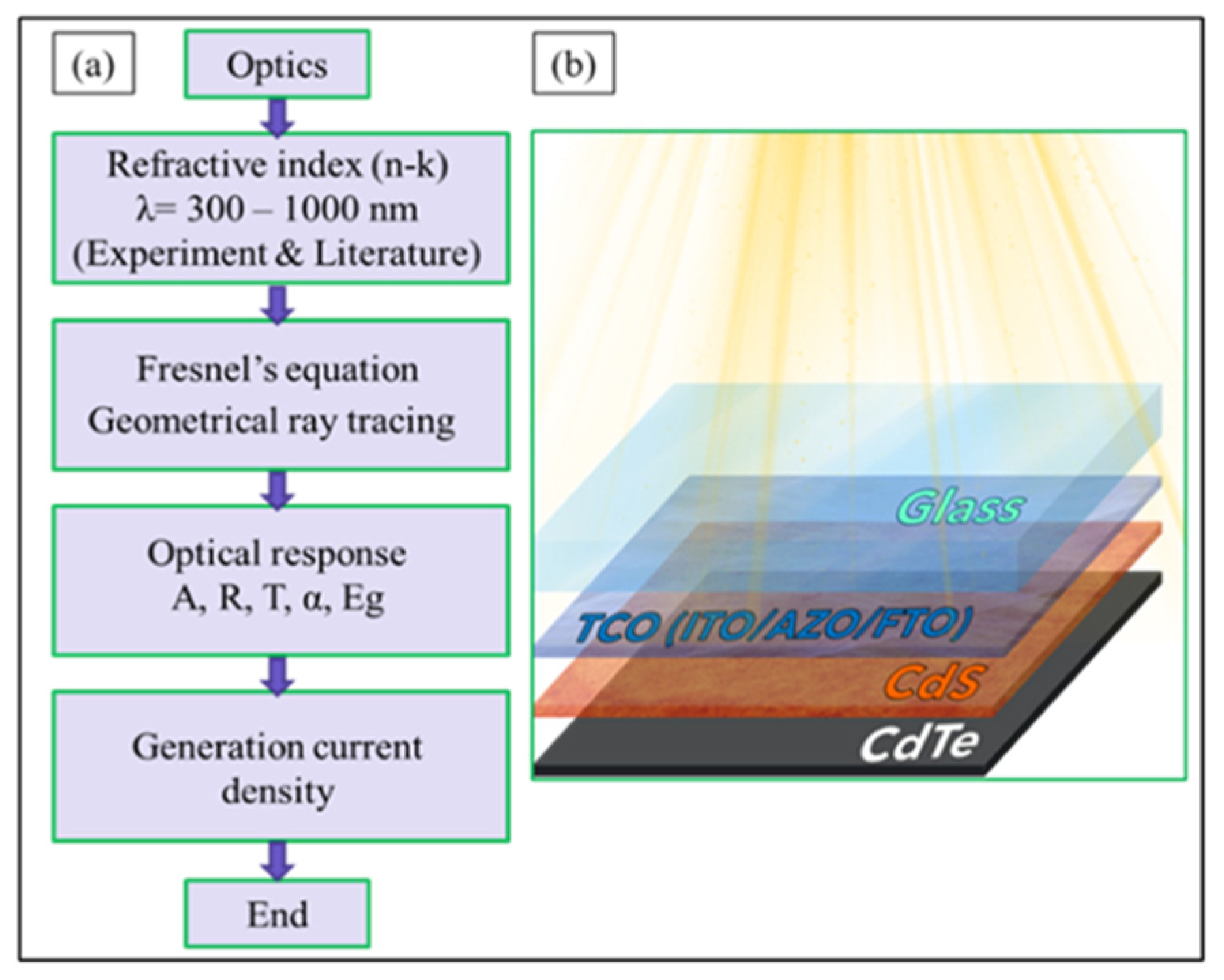
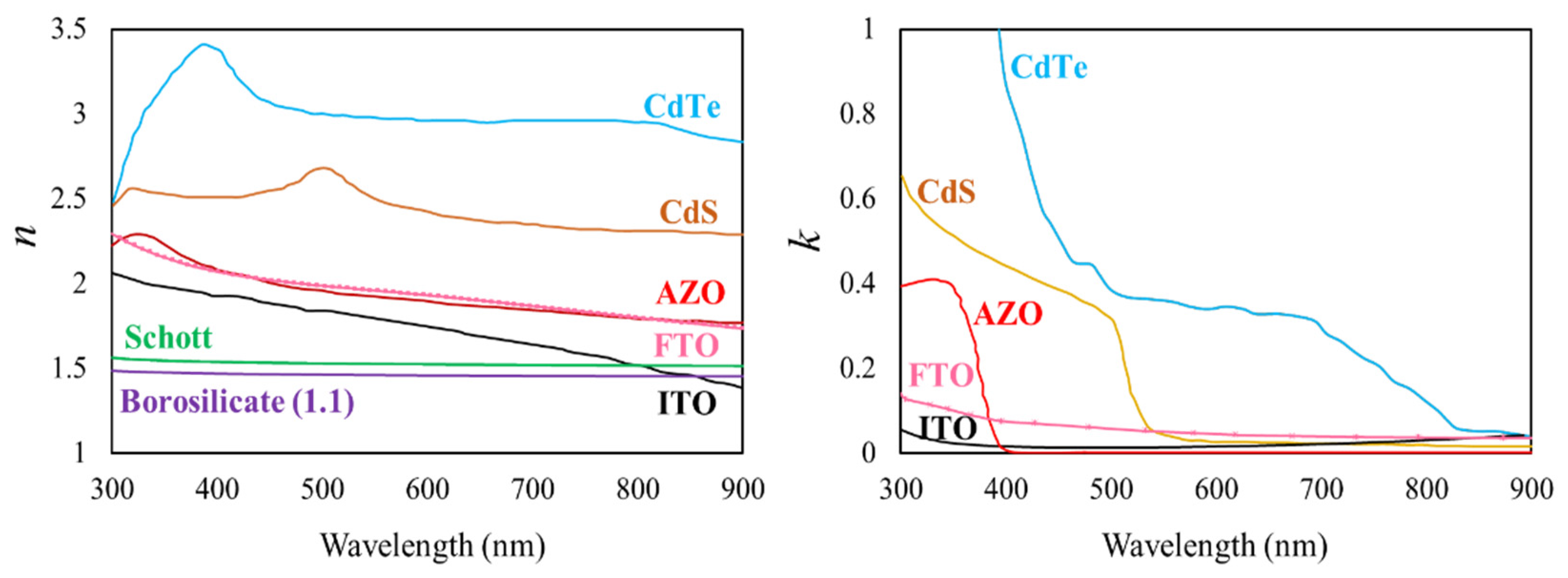
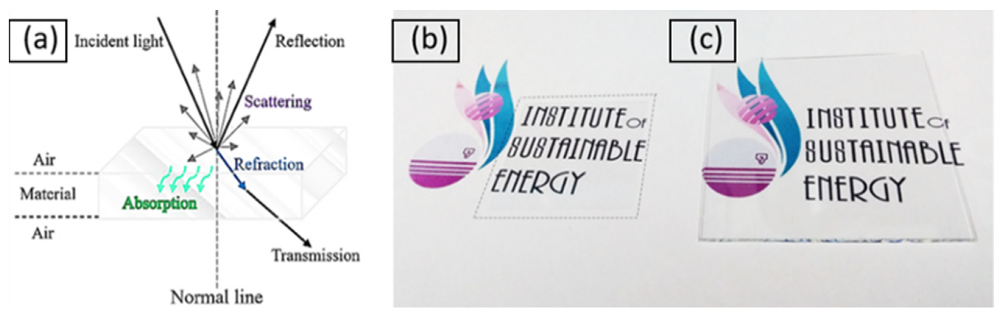
2. Simulation Method

The OPAL2 calculator (Version 2.6.1 from the Australian PV Lighthouse website) is built on the theory where the inbound ray to the textured surface interacts 2 or 3 times with the surface and analysis is based on Fresnel equations. For other modeling software, rays may be separated into a greater number of groups, requiring various equations to be solved for each ray interaction and taking a long processing time. The simplification in OPAL2 analysis decreases the simulation time significantly while providing accurate results. The OPAL2 optical simulator is used here to calculate the reflection, absorption, and transmission concerning the design requirements of flexible CdTe thin films [35]. Absorption, reflection, and transmission (ART) of light in the 300–900 nm spectrum range is determined considering the photon flux (Φ) in the AM1.5 g solar radiation [41]. The internal light trapping model is given by Equation (1), where Z is optical pathlength factor, α is absorption coefficient of the substrate, W is substrate thickness, and n indicates the refraction index of deposited material:
Z = 4 + {ln[n2 + (1 − n2) × e−4αW]}/αW
In 1982, Yablonovich used the theory of detailed balance of photons to provide this conclusion: In essence, no matter how clever or sophisticated the optical design, Z cannot exceed 4n2 based on ideal ergodic light scattering model [42]. D263T Schott flexible glass with 100 µm thickness is used in the modeling structure as the substrate to design the superstrate thin films. The thickness of the TCO and CdS layers as transparent oxide and window layer varied (30 to 300 nm).

3. Modelling Procedure

Modeling is necessary to interpret the advanced measurements on designing and optimization of solar cell structures [43]. Configuration of the thin-film structure without modeling will complicate the analytical process. OPAL2 as a freeware program offers accurate modeling of multiple interactions of incident light with material interfaces and accounts for complex refractive indices, analyzing the polarization of rays as they interact with cell structures [44]. It contains a large database of refraction and extinction coefficient for optical materials, extracted from scientific literature [45]. In this study, OPAL2 software is used to simulate the cell structure and calculate the ART values at every interaction of every ray using the refractive index and extinction coefficient values presented in Figure 2.
In contrast to other simulators, which take a long progress time calculating Fresnel equation for thin film designs, the Fresnel equations are determined in OPAL2 for each path as the numbers of paths in a thin film system are limited where all the rays on the same path represent the same faces at the same angles. Therefore, some paths are sub-sets of other paths and some that impact separate faces are also similar under some polarization. This solver measures the distribution of light through the transfer matrix (TMM) process in thin films [46].
  • The simulation platform OPAL2 was implemented for the assessment of reflectance/absorption and transmission, optical spectrum characteristics of various product layers, respectively.
  • A beam divides into a sequence of rays, such that the whole distance of the light window is filled by the number of rays.
  • The software addresses discontinuities in the limits of the unit dynamically as the beam is split.
  • Rays are also split into the emitted ray and the reflected ray at interfaces between the layers.
Polarization does not contribute strongly to an applied field in actual materials. This results in dielectric loss, which is quantified by the complex index of refraction. In every medium with complex refractive index n* = n + ik, where n presents the index of refraction, k is the extinction coefficient and i shows the square root of −1. The index’s real component explains the difference in velocity or wavelength of a wave propagating from a vacuum into a medium, whereas the imaginary part measures the wave’s dissipation rate in the medium. Basically, we can assume that n = n when only the real part of the refractive index is considered in the transparent region. However, at resonant frequencies along both sides of the transparency sphere, absorption becomes significant, and the imaginary part of the refractive index must be regarded so that n* = n + ik is utilized [47].
In this context, the corresponding thickness (nm), refractive index (n), extinction coefficient (k), and material name must be specified in OPAL. The transfer matrix equation detects the complex refractive index from the corresponding data file to compute the transmittance and reflectance. The flux of photons into each device may be controlled by the reflected flux that is emitted and consumed by each interface. Reflectance is given by [47]:
R = ( n 1 ) 2 ( n + 1 ) 2 = ( n 1 ) 2 + k 2 ( n + 1 ) 2 + k 2
The k or extinction coefficient value is an optical property, which presents the absorbed portion of the light by the surface. k > 0 means absorption, while k = 0 means the light travels straight through the material. Transmittance T, for a system of a weakly absorbing thin film (k2 << n2) on transparent substrate, is presented by:
T ( λ ) = ( 1 R 12 )   ( 1 R 23 )   ( 1 R 34 )   ( 1 R 45 ) × exp ( α Schglass d Schglass ) × exp ( α TCO d TCO )
where R shows the reflection coefficients, related to air, glass, TCO and CdS interfaces, respectively [48]. For the first interface between air and glass, the reflection coefficient and k value are supposed to be 1 for air [49]. The absorption coefficient is correlated with the wavelength of light and with another quantity called the extinction coefficient (related to electromagnetic rays from the sun).
α ( λ ) = 4 π λ k
Knowing the transmission of the glass, the spectral reliance of absorption coefficient αglass can be calculated. The small value of glass-based reflection R12 (about 4%) can be used to formulate αglass without assumption of several reflections from the layers in thin film structure [48]:
α glass = 1 d glass ln [ ( 1 R 12 ) 2 T ( λ ) ]
The generation current density, Jgen, reflects the photon current absorbed in the active region, presented by Equation (6). With constant setting values for W and Z(λ) (to be consistent with λ or at its ideal upper limit of Z = 4n(λ)2), using n as the real part of the refractive index [50]:
J gen = 200 1200 I ( λ )   [ 1 R ( λ ) A ( λ ) ] { 1 exp ( Z ( λ ) W α ( λ ) ) } d λ
In the concept of the optical carrier design, a range of planar adjacent layers are proposed, mounted by monochromatic plane waves with arbitrary angles of incidence. Each layer must be homogeneous, isotropic, and optically linear and the intensity of radiated and reflected, waves, on each surface, is determined using transfer matrices (TM). In addition, the interlayer oscillates as the function of thickness establishes a clear link with thickness dependency and fermi surface of the material using StandingWave command defining different adjacent layers. Coding and equations related to this method are presented elsewhere [51]. Reflectance, transmittance, and absorptance are calculated based on the defined wavelength-dependent complex, refractive index, and thickness consequently. Reflectance amplitudes and transmittances are turned into probabilities and a spontaneous, likely judgment is made to choose whether or not to reflect or to relay the ray at the interface. The gains (absorption or photogeneration) and losses (reflection, transmission, and parasitic absorption) are evaluated for each ray. Figure 3 shows the split rays propagate through the surface and split rays at an area interface between the emitted and reflected rays.
The simulation in OPAL2 requires user inputs for the surface condition, planar fraction dielectric film thicknesses, refractive index and extinction coefficient, substrate thickness, and light trapping model to define the generation current density (Jgen) within the wafer. In this research, all interfaces were assigned to be planar, since smooth and uniform solar designs may specifically improve light trapping, which is essential in CdTe films that rarely absorb near band wavelengths [52], as well as minimizing the front surface reflection [53]. The thickness of the glass for the first step of comparison was 0.1 mm compared with 1.1 mm glass. The refractive index profile of Schott ultra-thin glass was uploaded from the datasheet presented by the supplier. Half a million rays were traced over the wavelength range of 300 to 1000 nm and illumination source supposed to have uniform radiation and a normal incident of unpolarized AM1.5 g spectrum, beside neglecting the back stage losses. After the substrate comparison step and to check the optical properties of the proposed materials, all coated substrates are defined to be 0.1 mm thin glass as the top layer. Thickness of the coated ITO, CdS, and CdTe are varied for the sake of optimization, ultimately.

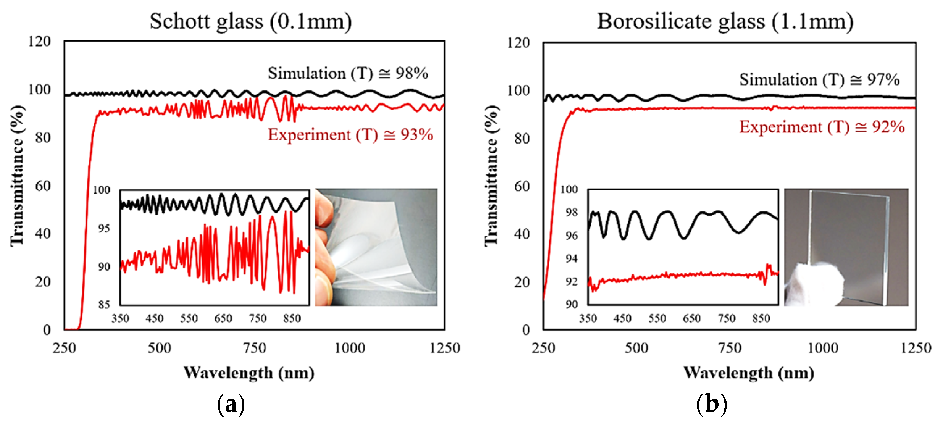
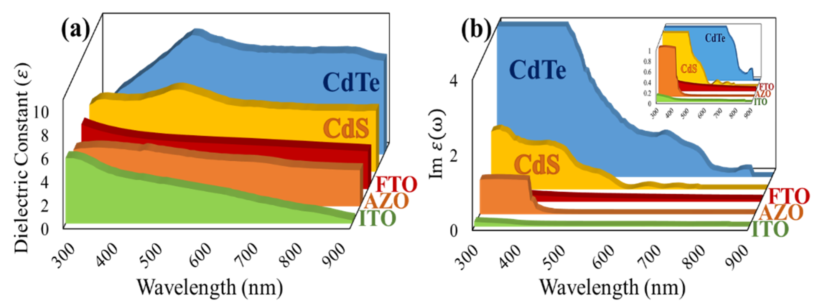
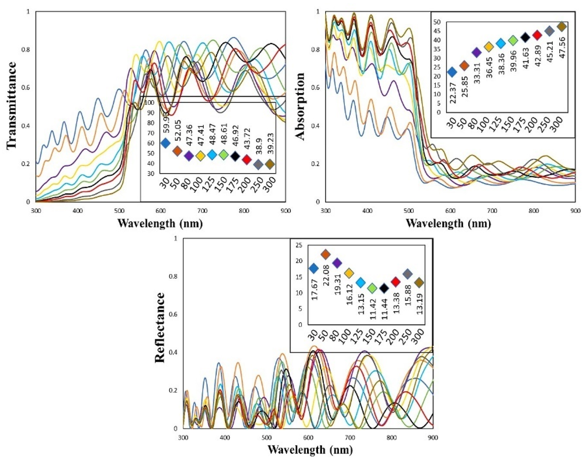
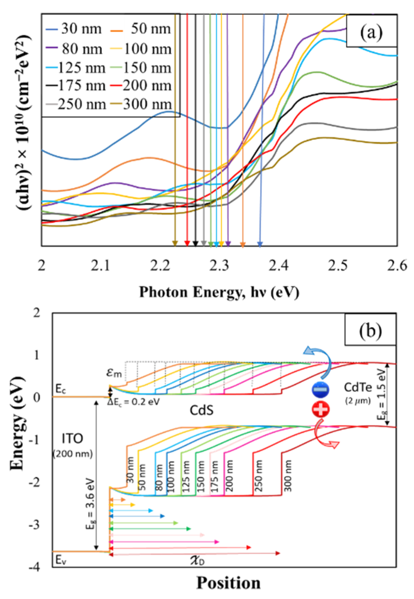
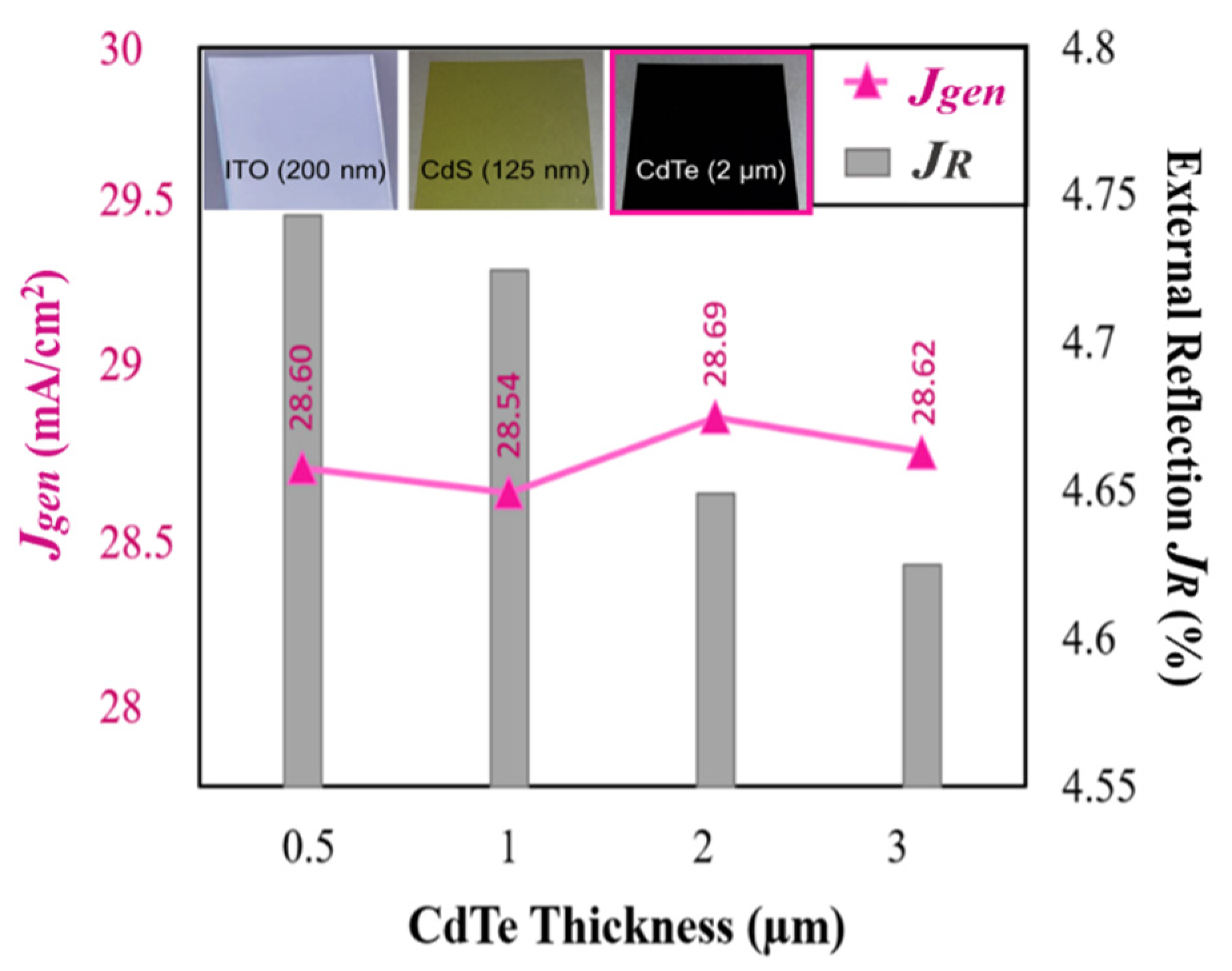
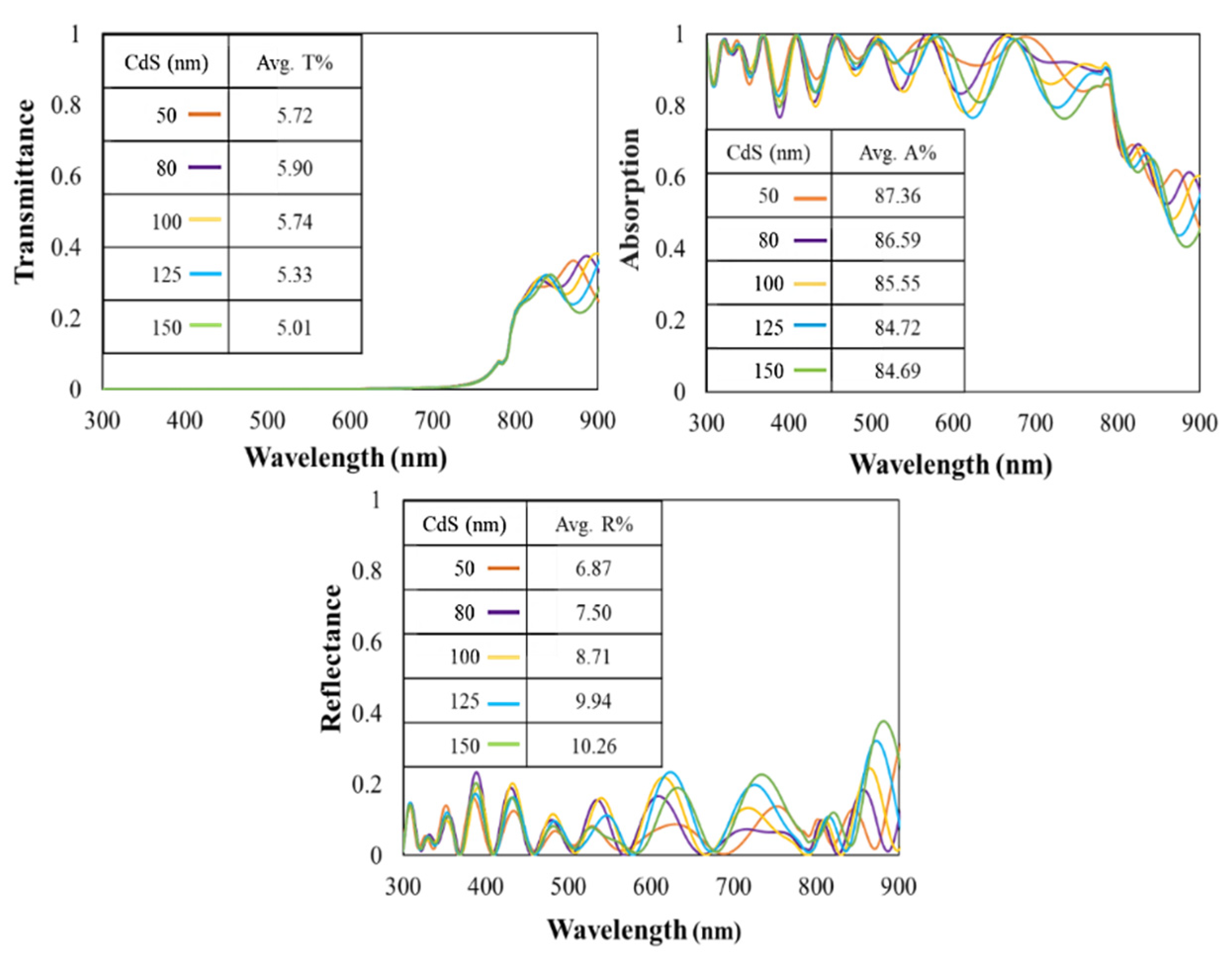
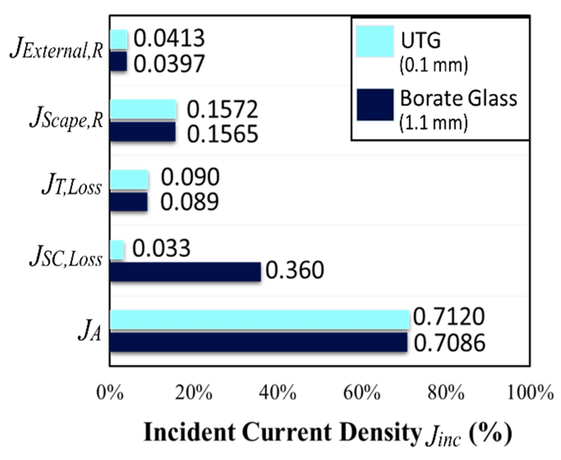
4. Modelling Analysis

As the main goal in this study, optical parameters are evaluated after adding every single layer to ensure accurate accounting for total internal reflection at the glass/air interface and the substrate thickness/material effect on the whole design [54]. Normally, to design an optimum CdTe structure, 1–2 μm CdTe absorber is favourable, which is hard to achieve due to high defect densities and photo-current losses [18]. The reason is that CdTe becomes thinner than photon absorption length and light passes through the back surface, leading to incomplete optical absorption (deep penetration loss) [55]. In thin film design, thickness related to each deposited layer plays a critical role in overall efficiency of the complete cell. Hence, it is important to compare layer by layer optical properties in respect to thickness [56]. The OPAL2 method is used here to calculate the spectral curves for ART data related to the glass/ITO and glass/ITO/CdS sub-cells for thickness optimization, in order to ensure efficient light absorption in the CdTe thin film.
Primarily, in order to inspect the accuracy of the simulation results, real-time optical analysis is conducted at normal incidence and room temperature on borosilicate and Schott glass. Experimental calculations were taken in a wavelength range of 300–900 nm using the (Lambda-35) UV–vis spectrophotometer. Figure 4 presents the experimental result versus the simulated transmittance for both 1.1 and 0.1 mm glass, showing that the transmittance value in borate glass starts from 200 nm and Schott glass covers the transmittance wavelength from 300 nm. The average transmittance in ultra-thin glass is about 1% higher than 1.1 borosilicate and the experimental and simulated results follow the same pattern. In addition, the amplitude and frequency of the fringes in Schott glass are almost twice higher compared to normal borosilicate substrate. In the transmission span of thin films, depending on clarity and thickness, typically some interference fringes take shape. Fringes emerge from lower wavelengths compared with the thick or deposited layer samples in the clearest and transparent surfaces and the extinction coefficient often represents this specification [57]. Two main properties affecting the amplitude and number of these ripples are the thickness and transparency of each layer [58]. Hence, fringes in Schott glass transmittance spectra indicate the smooth surface and high structural perfection of the ultra-thin glass compared to standard substrates [54].
Here is the analysis related to the TCO layer as the frontal contact and the second interface that permits light. In OPAL simulation, the surrounding is proposed as air and the thin film is designed in superstrate configuration in the current study. In addition, the reflection from glass is considered to be effective [35]. Adding a TCO layer on bare glass, total transmittance decreases due to increased absorption in the deposited layer on the transparent substrate.
Figure 5 illustrated the ART parameters in respect to three different TCO materials. The TCO layer absorbs the spectrum, both in the UV above their bandgaps and in the IR due to excitation of free carriers [58]. The maxima and minima (dsinθ = nλ) and (dsinθ = (n + 1/2) × λ), where path difference is nλ, diffraction angle is θ, and slit width is d, are due to the interference of light and their positions and number of ripples depend on film thickness [59]. In Figure 5, although AZO presented the lowest absorption in the 400 to 900 nm range, the highest transmittance, as well as reflection results in average is obtained from ITO data analysis. FTO is extremely affected by the thickness variation [60]. For the 100 nm sample, there were clear and distinct interference fringes with relatively large intensity above 80%. At the fundamental absorption edge of the film, the sensitivity of the fringes of interference decreases in magnitude towards the null value.
The frequency of fringes in the transmission depends solely on the thickness of the film and the appearance of adequate fringes pattern in the transmittance spectra of the samples revealed good surface coverage in respect to thickness [61,62]. The optical absorption edges are red-shifted as the thickness increased from 100 to 500 nm, while specifying the reduction in bandgap energy values [63], as presented in Figure 6. The results are in good agreement with [17,37]. In respect to software equations and TMM method coding, these fringes are related to the implementation of the scattering effects due to the difference of the refractive index values at the interfaces [64,65]. Changes in thickness resulted in the reflectance curve having different interference fringe patterns attributed to the carrier density change in various thickness ranges [66]. If the carrier concentration rises, the height of the absorbing band increases in contrast to the half-width value related to the absorption band’s diameter that declines with thickness, and the absorption curve peak moves through shorter wavelengths for thinner samples [16]. In total, the behavior of the transmission spectrum affected by the thin film thickness for ITO, AZO, and extreme changes observed for FTO, which was the effect of the number of interference fringes and depth of these fringes and optical transmittance, varies adversely with the thickness range. ITO films show high optical transmittance between 80% and 85% for samples thinner than 300 nm. In addition, ITO thickness 200 nm and below show more stable results and Fresnel reflection increases as the refractive index difference between two layers/materials increases, in respect to the TCO material used [67]. Therefore, samples with 200 nm ITO would be the optimum choice to reduce Fresnel reflection. Absorption plots show higher absorption in the UV range related to excitations across the fundamental energy bands. Therefore, the next evaluation steps are conducted using 200 nm TCO material as the optimum choice for TCO material in flexible CdTe design [68,69].
In solar cell design, configuration of the ITO layer is not just a highly transparent material over the visible light region; high conductivity is also required. Figure 7 shows the real and imaginary dielectric constant (ε) for each TCO material [70], determined using Equation (7); the TCO layer is assumed to have optimum thickness of 200 nm.
ε ( ω ) = ε R ( ω ) + ε I ( ω )
ε R = n 2 k 2
In principle, the real value of the dielectric constant refers exactly to the refractive index. The measured actual dielectric constants plotted in Figure 7a show a complete red shift for various TCO materials. Extreme reduction occurred in the real dielectric constant for ITO after the 400 nm, whereby the samples having AZO and FTO as the TCO layer exhibited a slight decrease in real dielectric constant throughout the plotted wavelengths. It confirms that the refractive index is directly impacted by the real part of the dielectric constant and the ITO layer is a great choice for the UTG substrate by matching refractive index data with the Schott glass. Moreover, the imaginary part of the dielectric constant of TCO layers is evaluated by Equation (9):
ε I = n 2 k 2
The variations in the imaginary part of the dielectric constant of TCO with respect to the incident photon wavelength are framed in Figure 7b. In principle, the imaginary component is absorbance in the dielectric constant. Here, the calculated imaginary dielectric constants with the red-shift for each TCO material proves that the absorbance is dependent on the imaginary part of the dielectric constant and the lowest absorbance value is related to the ITO material. In addition, at room temperature, the transparency and uniformity of the ITO are better compared to the SnO2:F [71]. From the presented analysis, the 200 nm ITO layer shows the most stable properties to make an optimum CdTe cell structure [72].
Following the thin film design steps, the CdS layer is added to the structure to study the effect of the window layer. In general, the input light is such that the current density of the structure corresponds to 30 mA/cm2 for 100% transmission to the CdTe absorber part. Accordingly, on average, 25% of this input light is absorbed in the ITO/glass front sub-cell (illustrated in Figure 5), which corresponds to 8 mA/cm2 of output current density from the cell. In addition, the effect of the CdS layer thickness ranging from 30 to 300 nm proposed on ITO (200 nm)/UTG is presented in Figure 8. ART values in Figure 8 show the average transmittance of 40% to 60% transmitted current density portion; about 20 mA/cm2 depending on the CdS layer thickness is transmitted from the front surface to the absorber and the remaining 2 mA/cm2 or 5% is absorbed in the front glass. The reflectance ripples in the visible range or Fabry-Perot fringes are induced by the layers’ interaction and normally observed for samples where the deposited layer and substrate material are not the same [73]. This method is favorable to minimize the light reflections within interfaces while making a uniform hole-free deposition CdS deposition range below 200 nm and above 50 nm.
The ART parameter results, as shown in Figure 8, follow almost the same pattern for all the CdS thickness range, except for the position of the fringes, which shifted higher; the absorption in the blue region also increases drastically with rise in thickness. Accordingly, the band diagram results in Figure 9a show that the light transmittance or penetration in the CdS layer at 50 to 150 nm is within the acceptable range (high transparency) while having a compatible bandgap above 2.3 eV.
Under forward bias, the contact potential difference, presenting the degree of energy-band bending, corresponding to the current transport system in the interface, is plotted in Figure 9b:
V D = ( ε m X D ) / 2
A favourable potential barrier height or contact difference is known to be in range of 0.2 to 0.4 eV, achieved using 80 to 150 nm CdS material (presented in Figure 9b). Following the VD equation, sufficient band bending shapes with a depletion region of ~1 µm having a CdS layer of 80 to 150 nm to improve the carrier transport are seen. Further increase in CdS layer thickness (>150 nm) leads to poor performance in the CdS/CdTe interface, carrier recombination, and small electric field intensity, which is an indication of more diffusive electron movements [74]. The aim in optical optimization of the fore layers is to transfer the maximum possible spectrum to the CdTe absorber. Using the thinner CdS layers increases the Jsc slightly (about 3%), whereas the thick CdS layer also boosts the junction composition and decreases defect densities at the interface. This implies that at the manufacturing level, the CdS layer within the 80 to 150 nm range might be effective to satisfy both benefits [75]
Considering the CdTe layer thickness, reduction of the absorber layer thickness to 0.5 µm, as a substance used in thin film and solar module production, obviously decreases the use of CdTe up to about five times, compared to the conventional modules. However, the deposition of an extremely thin absorber layer may cause faulty coverage with too many pinholes and under-ranged electrical properties. Therefore, the selection of the golden extent to ensure the CdS/CdTe modules provide the best quality and consumption of the content is critical. According to a study by Kosyachenko et al., with dCdTe ≥ 5 µm, the total losses are 3%–4%, but while thinning the CdTe layer up to 0.5 µm, the losses increase to ~20% [48]. This way, another evaluation to check the optimum thickness range for flexible CdTe thin films is presented in Figure 10, by calculation of the reflection (JR) and generation current (Jgen) for various CdTe layer thicknesses.
The results show that the optimum design for a flexible CdTe film is possible using minimum 2 μm thickness and on ultra-thin glass with reflection of about 4.6% and highest generation or short circuit current of 28.69 mA/cm2, leading to high-efficiency flexible CdTe thin film design [76]. Ultimately, optimal thickness of 2 µm CdTe is added to the fixed frontal layers of UTG/ITO (200 nm)/CdS (50 to 150 nm), as presented in Figure 11.
Using standard conditions (AM 1.5G spectrum, 100 mW/cm2, 25 °C), the overall performance of the optimum CdTe cell structure on UTG and standard glass substrate is studied. OPAL provides all the losses as well as the absorbance in both designs (UTG integrated model and standard borosilicate substrate design). Comparative outputs illustrated in Figure 12 show about 1% increase in thin film efficiency using UTG substrates and less reflectance due to the highly smooth and treated surface of UTG.
There is a slight change in losses, such as higher external/scape reflections using UTG because of the smooth surface, and more absorbance in the absorber layer due to higher JSC that results in a higher efficiency design; the short circuit current or the photon current absorbed in the active region, which is due to the strong electric field acting on the CdTe layer near the front surface (close to CdS), preventing carriers produced on the surface from being combined [48]. In summary, using the highly transparent UTG model, three promising conducting oxides, analyzed for their optoelectrical features and 200 nm ITO, proved to have potential as a TCO layer. The window layer study is presented afterward, and the 30 to 300 nm CdS layer defined in OPAL2 on a 200 nm ITO coated substrate and inspections resulted in 50 to 150 nm of CdS to act as a suitable hetero face for the CdTe absorber layer. The CdTe layer is designated and varied by thickness to evaluate the current transfer and loss of the proposed layers and efficiency of the fully stacked CdTe thin film. Ultimately, a favorable structure resulted from the OPAL2 calculations, and was defined and evaluated on standard and ultra-thin glass, showing 1% overall boosted efficiency using Schott UTG specifications in a simulation work. Overall, the OPAL2 calculator offers the possibility to upload the Internal Quantum Efficiency (IQE), absorption coefficient, refractive index, and extinction coefficient parameters for up to three materials, instead of full assumption-based methods that may lead to inaccurate predictions. However, it is not possible to analyse the interfacial effects, textured designs, and other complex thin film designs, such as tandem solar cells, using this method.

5. Conclusions

An analytical approximation of the profile of photogeneration on the top of a uniform, planar CdTe thin film is thoroughly studied in this paper using Ray tracing and OPAL2 modeling platforms. A transmittance parameter relative to the ultra-thin glass and standard glass substrate is physically evaluated using UV-Vis (Lambda-35), and the results are compared with the outputs from the OPAL2 to check for matching patterns and ensure the accuracy of the modeled design presented in this work. The optical characteristics (RAT) of various transparent conducting oxide (TCO) materials placed on 0.1 mm substrate of ultra-thin Schott glass revealed ITO (200 nm thickness) as the optimum choice. Consequently, favourable thickness for both n and p layers in the proposed configuration was found to be 50 to 150 nm for the CdS layer and a minimum of 2-micron of the CdTe absorber layer to achieve the highest short circuit current of 28.69 mA/cm2. However, further investigation is recommended with an emphasis on chemical and mechanical characteristics found from various deposition methods of the layers to optimize the design configuration. Moreover, quality and stability control tests would be beneficial in order to confirm the viable guidelines and requirements in effective thin film design and production.

Author Contributions

Conceptualization, N.A.; data curation, N.A.; formal analysis, N.A.; funding acquisition, Z.A.A.; methodology, N.A.; investigation, N.A.; project administration, N.A., M.R.K. and Z.A.A.; writing—original draft preparation, N.A.; writing—review and editing, N.A.; visualization, M.R.K. and Z.A.A.; validation, N.A.; supervision, N.A., M.R.K. and Z.A.A. All authors have read and agreed to the published version of the manuscript.

Funding

This project was funded by the National Plan for Science, Technology, and Innovation (MAARIFAH), King Abdul Aziz City for Science and Technology, Kingdom of Saudi Arabia, award No. 13-ENE2229-02.

Institutional Review Board Statement

Not applicable.

Informed Consent Statement

Not applicable.

Data Availability Statement

Not applicable.

Acknowledgments

The authors acknowledge the National Plan for Science, Technology, and Innovation (MAARIFAH), King Abdulaziz City for Science and Technology, Kingdom of Saudi Arabia for its grant with award No. 13-ENE2229-02.

Conflicts of Interest

The authors declare no conflict of interest.

References

  1. Shah, A. Thin-Film Silicon Solar Cells; CRC Press: Boca Raton, FL, USA, 2010. [Google Scholar]
  2. Ojo, A.A.; Cranton, W.M.; Dharmadasa, I.M. Next Generation Multilayer Graded Bandgap Solar Cells; Springer: Cham, Switzerland, 2019. [Google Scholar]
  3. Krc, J. Optical Modeling and Simulation of Thin-Film Photovoltaic Devices; CRC Press: Boca Raton, FL, USA, 2013. [Google Scholar]
  4. Daniel, M.M.; Matthew, O.R.; Charles, W.W.; Ali, A.; James, M.B.; Hasitha, P.M.; Wyatt, K.M.; John, M.W.; Mark, C.L.; Teresa, M.B.; et al. Evolution of oxygenated cadmium sulfide (CdS:O) during high-temperature CdTe solar cell fabrication. Sol. Energy Mater. Sol. Cells 2016, 157, 276–285. [Google Scholar]
  5. Bosio, A.; Pasini, S.; Romeo, N. The history of photovoltaics with emphasis on CdTe solar cells and modules. Coatings 2020, 10, 344. [Google Scholar] [CrossRef] [Green Version]
  6. Kranz, L.; Schmitt, R.; Gretener, C.; Perrenoud, J.; Pianezzi, F.; Uhl, A.R.; Keller, D.; Buecheler, S.; Tiwari, A.N. Progress towards 14% efficient CdTe solar cells in substrate configuration. In Proceedings of the 39th IEEE Photovoltaics Specialists Conference, Tampa, FL, USA, 16–21 June 2013; pp. 1644–1648. [Google Scholar]
  7. Mohamed, H.; Hadia, N. Theoretical analysis of ZnO and ZnO based alloys as front electrode in CdS/CdTe solar cells. Optics 2015, 126, 1976–1980. [Google Scholar] [CrossRef]
  8. Drăgan, F.; Nordseth, Ø.; Fara, L.; Dumitru, C.; Crăciunescu, D.; Muscurel, V.; Sterian, P. Optical modeling and simulation of tandem metal oxide solar cells. Ann. West Univ. Timisoara. Phys. Ser. 2018, 60, 56–66. [Google Scholar] [CrossRef] [Green Version]
  9. Rance, W.L.; Burst, J.M.; Meysing, D.M.; Wolden, C.A.; Reese, M.O.; Gessert, T.A.; Metzger, W.K.; Garner, S.; Cimo, P.; Barnes, T.M. 14%-efficient flexible CdTe solar cells on ultra-thin glass substrates. Appl. Phys. Lett. 2014, 104, 143903. [Google Scholar] [CrossRef]
  10. Salavei, A.; Menossi, D.; Piccinelli, F.; Kumar, A.; Mariotto, G.; Barbato, M.; Meneghini, M.; Meneghesso, G.; Di Mare, S.; Artegiani, E.; et al. Comparison of high efficiency flexible CdTe solar cells on different substrates at low temperature deposition. Sol. Energy 2016, 139, 13–18. [Google Scholar] [CrossRef]
  11. Hojo, J. Materials Chemistry of Ceramics; Springer Nature: Fukuoka, Singapore, 2019. [Google Scholar]
  12. Brusberg, L.; Henning, S.; Michael, T.; Herbert, R. Photonic system-in-package technologies using thin glass substrates. In Proceedings of the 11th Electronics Packaging Technology Conference, Singapore, 9–11 December 2009; pp. 930–935. [Google Scholar]
  13. Cvecek, K.; Johannes, H.; Isamu, M.; Michael, B. Dominique de, L.; Michael, S. On-line interferometric observation of thermomechanically induced refractive index changes during glass welding by ultra-short laser pulses. J. Laser Micro Nanoeng. 2018, 13, 301–308. [Google Scholar]
  14. Ikhmayies, S.J. Transparent conducting oxides for solar cell applications. In Mediterranean Green Buildings & Renewable Energy; Springer: Berlin/Heidelberg, Germany, 2017; pp. 899–907. [Google Scholar]
  15. Ferekides, C.S.; Mamazza, R.; Balasubramanian, U.; Morel, D.L. Transparent conductors and buffer layers for CdTe solar cells. Thin Solid Film. 2005, 480, 224–229. [Google Scholar] [CrossRef]
  16. Coutts, T.J.; Young, D.L.; Gessert, T.A. Modeling, characterization, and properties of transparent conducting oxides. In Handbook of Transparent Conductors; Springer: Boston, MA, USA, 2011. [Google Scholar]
  17. Ngamsinlapasathian, S.; Sreethawong, T.; Suzuki, Y.; Yoshikawa, S. Doubled layered ITO/SnO2 conducting glass for substrate of dye-sensitized solar cells. Sol. Energy Mater. Sol. Cells 2006, 90, 2129–2140. [Google Scholar] [CrossRef]
  18. Kumar, S.G.; Rao, K.R.S.K. Physics and chemistry of CdTe/CdS thin film heterojunction photovoltaic devices: Fundamental and critical aspects. Energy Environ. Sci. 2014, 7, 45–102. [Google Scholar] [CrossRef]
  19. Khusayfan, N.M.; El-Nahass, M.M. Study of Structure and electro-optical characteristics of indium tin oxide thin films. Adv. Condens. Matter Phys. 2013, 2013, 408182. [Google Scholar] [CrossRef] [Green Version]
  20. Parsianpour, E.; Raoufi, D.; Roostaei, M.; Sohrabi, B.; Samavat, F. Characterization and structural property of indium tin oxide thin films. Adv. Mater. Phys. Chem. 2017, 7, 42–57. [Google Scholar] [CrossRef] [Green Version]
  21. Kurdesau, F.; Khripunov, G.; da Cunha, A.; Kaelin, M.; Tiwari, A. Comparative study of ITO layers deposited by DC and RF magnetron sputtering at room temperature. J. Non Cryst. Solids 2006, 352, 1466–1470. [Google Scholar] [CrossRef]
  22. John, K.A.; Philip, R.R.; Sajan, P.; Manju, T. In situ crystallization of highly conducting and transparent ITO thin films deposited by RF magnetron sputtering. Vacuum 2016, 132, 91–94. [Google Scholar] [CrossRef]
  23. Gordon, R.G. Criteria for choosing transparent conductors. MRS Bull. 2000, 25, 52–57. [Google Scholar] [CrossRef] [Green Version]
  24. Natarajan, P.; Vaiude, D.; Rao, B. Development/study of thin films for electroluminescent flat panel display. Microelectron. Int. 1992, 9, 28–32. [Google Scholar] [CrossRef]
  25. Junghähnel, M.; Weller, S.; Gebel, T. P-65: Advanced processing of ITO and IZO thin films on flexible glass. In Proceedings of the SID Symposium Digest of Technical Papers, San Jose, CA, USA, 21 May–5 June 2015; pp. 1378–1381. [Google Scholar]
  26. Yoo, J.-H.; Matthews, M.; Ramsey, P.; Barrios, A.C.; Carter, A.; Lange, A.; Bude, J.; Elhadj, S. Thermally ruggedized ITO transparent electrode films for high power optoelectronics. Opt. Express 2017, 25, 25533–25545. [Google Scholar] [CrossRef]
  27. Winkler, M.T.; Wei, W.; Gunawan, O.; Hovel, H.J.; Todorov, T.K.; Mitzi, D.B. Optical designs that improve the efficiency of Cu2 ZnSn(S,Se)4 solar cells. Energy Environ. Sci. 2014, 7, 1029–1036. [Google Scholar] [CrossRef]
  28. Benoy, M.; Mohammed, E.; Babu, M.S.; Binu, P.; Pradeep, B. Thickness dependence of the properties of indium tin oxide (ITO) FILMS prepared by activated reactive evaporation. Braz. J. Phys. 2009, 39, 629–632. [Google Scholar] [CrossRef] [Green Version]
  29. Cozza, D.; Ruiz, C.M.; Duché, D.; Giraldo, S.; Saucedo, E.; Simon, J.J.; Escoubas, L. Optical modeling and optimizations of Cu2ZnSnSe4 solar cells using the modified transfer matrix method. Opt. Express 2016, 24, A1201–A1209. [Google Scholar] [CrossRef]
  30. Cozza, D. Modeling and Physical Studies of Kesterite Solar Cells. Ph.D. Thesis, Aix Marseille, Marseille, France, 2016. [Google Scholar]
  31. McIntosh, K.R.; Abbott, M.D.; Sudbury, B.A.; Manzoor, S.; Yu, Z.J.; Mehdi, L.; Shi, J.; Holman, Z.C. Absorption in each layer of a silicon heterojunction solar cell. In Proceedings of the 2017 IEEE 44th Photovoltaic Specialist Conference (PVSC), Washington, DC, USA, 25–30 June 2017; pp. 1322–1328. [Google Scholar]
  32. Holman, Z.C.; Filipič, M.; Lipovšek, B.; De Wolf, S.; Smole, F.; Topic, M.; Ballif, C. Parasitic absorption in the rear reflector of a silicon solar cell: Simulation and measurement of the sub-bandgap reflectance for common dielectric/metal reflectors. Sol. Energy Mater. Sol. Cells 2014, 120, 426–430. [Google Scholar] [CrossRef]
  33. Barraud, L.; Holman, Z.C.; Badel, N.; Reiss, P.; Descoeudres, A.; Battaglia, C.; De Wolf, S.; Ballif, C. Hydrogen-doped indium oxide/indium tin oxide bilayers for high-efficiency silicon heterojunction solar cells. Sol. Energy Mater. Sol. Cells 2013, 115, 151–156. [Google Scholar] [CrossRef] [Green Version]
  34. Sabory-Garcia, R.A.; Leal-Cruz, A.L.; Vera-Marquina, A.; Garcia-Delgado, L.A.; Garcia-Juarez, A.; Rojas-Hernandez, A.G. modeling and analytical study for efficiency improvement for thin film solar cells based on CdS/PbS, CdS/CdTe, AND CdS/CdSe. Chalcogenide Lett. 2018, 15, 625–638. [Google Scholar]
  35. McIntosh, K.R.; Baker-Finch, S.C. OPAL 2: Rapid optical simulation of silicon solar cells. In Proceedings of the 2012 38th IEEE Photovoltaic Specialists Conference, Austin, TX, USA, 3–8 June 2012; pp. 265–271. [Google Scholar]
  36. Valencia, H.; Moreno, L.; Ardila, A. Structural, electrical and optical analysis of ITO thin films prepared by sol–gel. Microelectron. J. 2008, 39, 1356–1357. [Google Scholar] [CrossRef]
  37. Coutts, T.J.; Young, D.L.; Li, X. Characterization of transparent conducting oxides. MRS Bull. 2000, 25, 58–65. [Google Scholar] [CrossRef]
  38. Li, Q.H.; Zhu, D.; Liu, W.; Liu, Y.; Ma, X.C. Optical properties of Al-doped ZnO thin films by ellipsometry. Appl. Surf. Sci. 2008, 254, 2922–2926. [Google Scholar] [CrossRef]
  39. Winter, M.; Vogt, M.R.; Holst, H.; Altermatt, P.P. Combining structures on different length scales in ray tracing: Analysis of optical losses in solar cell modules. Opt. Quantum Electron. 2015, 47, 1373–1379. [Google Scholar] [CrossRef]
  40. Rashwan, O.; Newill, A.; Najan, N.K.K. Optimization of the light trapping nano structures in CdTe thin film solar cells. In Proceedings of the 2019 IEEE 46th Photovoltaic Specialists Conference (PVSC), Chicago, IL, USA, 6 February 2020; pp. 911–914. [Google Scholar]
  41. Nykyruy, L.; Yavorskyi, R.; Zapukhlyak, Z.; Wisz, G.; Potera, P. Evaluation of CdS/CdTe thin film solar cells: SCAPS thickness simulation and analysis of optical properties. Opt. Mater. 2019, 92, 319–329. [Google Scholar] [CrossRef]
  42. Khan, M.R.; Wang, X.; Alam, M.A. Fundamentals of PV efficiency: Limits for light absorption. arXiv 2012, arXiv:1212:2879. [Google Scholar]
  43. Slauch, I.M.; Deceglie, M.G.; Silverman, T.J.; Ferry, V.E. Two-layer anti-reflection coatings with optimized sub-bandgap reflection for solar modules. In New Concepts in Solar and Thermal Radiation Conversion and Reliability; International Society for Optics and Photonics: San Diego, CA, USA, 2018; Volume 10759, p. 1075911. [Google Scholar]
  44. Li, Y.; Li, Z.; Lu, Z.; Cui, J.; Ouyang, Z.; Lennon, A. Optical modelling for multilayer and geometric light-trapping structures for crystalline silicon solar cells. In Proceedings of the 2014 IEEE 40th Photovoltaic Specialist Conference (PVSC), Denver, CO, USA, 8–13 June 2014; pp. 1223–1226. [Google Scholar]
  45. Babkair, S.S.; Al-Twarqi, M.N.; Ansari, A.A. Optical characterization of CdTe films for solar cell applications. Karachi Univ. J. Sci. 2011, 39, 1–5. [Google Scholar]
  46. Kosyachenko, L.A. Possibilities to decrease the absorber thickness reducing optical and recombination losses in CdS/CdTe solar cells. Mater. Renew. Sustain. Energy 2013, 2, 14. [Google Scholar] [CrossRef] [Green Version]
  47. Fleischer, K.; Norton, E.; Mullarkey, D.; Caffrey, D.; Shvets, I.V. Quantifying the performance of P-type transparent conducting oxides by experimental methods. Materials 2017, 10, 1019. [Google Scholar] [CrossRef] [Green Version]
  48. Baker-Finch, S.C.; McIntosh, K.R. A freeware program for precise optical analysis of the front surface of a solar cell. In Proceedings of the 2010 35th IEEE Photovoltaic Specialists Conference, Honolulu, HI, USA, 1 November 2010; pp. 002184–002187. [Google Scholar]
  49. Sentaurus Device Monte Carlo/S-Band Version K-2015.06 User’s Manual, Synopsys, Inc., 2015. Available online: http://www.synopsys.com (accessed on 7 April 2021).
  50. Manzoor, S.; Zhengshan, J.Y.; Ali, A.; Ali, W.; Bush, K.A.; Palmstrom, A.F.; Bent, S.F.; McGehee, M.D.; Holman, Z.C. Improved light management in planar silicon and perovskite solar cells using PDMS scattering layer. Sol. Energy Mater. Sol. Cells 2017, 173, 59–65. [Google Scholar] [CrossRef]
  51. Product Variants of D263. Available online: https://www.schott.com/en-us/search?q=Product%20variants%20of%20D263 (accessed on 20 May 2020).
  52. Rangel-Cárdenas, J.; Sobral, H. Optical absorption enhancement in CdTe thin films by microstructuration of the silicon substrate. Materials 2017, 10, 607. [Google Scholar] [CrossRef] [Green Version]
  53. Khomyak, V.V.; Slyotov, O.M.; Chupyra, S.M. Optical and photoluminescence properties of ZnO1−xSex thin films. Appl. Opt. 2014, 53, B110–B115. [Google Scholar] [CrossRef] [PubMed]
  54. Arfsten, N. Sol-gel derived transparent IR-reflecting ITO semiconductor coatings and future applications. J. Non Cryst. Solids 1984, 63, 243–249. [Google Scholar] [CrossRef]
  55. Tehrani, F.S.; Fakhredin, M.; Tafreshi, M.J. The optical properties of silicon carbide thin films prepared by HWCVD from pure silane and methane under various total gas partial pressure. Mater. Res. Express 2019, 6, 086469. [Google Scholar] [CrossRef]
  56. Laureto, E.; da Silva, M.A.T.; Fernandes, R.V.; Duarte, J.L.; Dias, I.F.L.; Marletta, A. Thickness effects on the optical properties of layer-by-layer poly (p-phenylene vinylene) thin films and their use in energy-modulated structures. Curr. Appl. Phys. 2012, 12, 870–874. [Google Scholar] [CrossRef]
  57. Ikhmayies, S.J. Thickness Dependence of the optical parameters of spray-deposited SnO2:F thin films. In Proceedings of the TMS 2015 144th Annual Meeting & Exhibition, Orlando, FL, USA; 2015; pp. 593–600. [Google Scholar]
  58. Asl, H.Z.; Rozati, S.M. High-quality spray-deposited fluorine-doped tin oxide: Effect of film thickness on structural, morphological, electrical, and optical properties. Appl. Phys. A 2019, 125, 689. [Google Scholar] [CrossRef]
  59. Emam-Ismail, M.; El-Hagary, M.; Shaaban, E.; Al-Hedeib, A. Microstructure and optical studies of electron beam evaporated ZnSe1−xTex nanocrystalline thin films. J. Alloy. Compd. 2012, 532, 16–24. [Google Scholar] [CrossRef]
  60. Vasiliev, M.; Belotelov, V.; Alameh, K. Properties of ferrite garnet (Bi,Lu,Y)3(Fe,Ga)5O12 thin film materials prepared by RF magnetron sputtering. Nanomaterials 2018, 8, 355. [Google Scholar]
  61. Ghorannevis, Z.; Akbarnejad, E.; Ghoranneviss, M. Structural and morphological properties of ITO thin films grown by magnetron sputtering. J. Theor. Appl. Phys. 2015, 9, 285–290. [Google Scholar] [CrossRef] [Green Version]
  62. Han, X.; Mendes, S.B. Spectroelectrochemical properties of ultra-thin indium tin oxide films under electric potential modulation. Thin Solid Films 2016, 603, 230–237. [Google Scholar] [CrossRef] [Green Version]
  63. Rabeh, M.B.; Khedmi, N.; Fodha, M.A.; Kazari, M. The effect of thickness on optical band gap and N-type conductivity of CuInS2 thin films annealed in air atmosphere. Energy Procedia 2014, 44, 52–60. [Google Scholar] [CrossRef] [Green Version]
  64. Yang, T.C.-J.; Lin, R.; Lin, Z.; Zhang, T.; Wu, L.; Jia, X.; Puthen-Veettil, B.; Perez-Wurfl, I.; Conibeer, G. Investigation into high temperature post-annealing of ZNO:Al as a prospective transparent conductive oxide window layer for superstrate silicon nanostructure solar cells. In Proceedings of the 1BV.7 New Materials and Concepts for Cells, Amsterdam, The Netherlands, 23 September 2014. [Google Scholar]
  65. Yan, X.; Mont, F.W.; Poxson, D.J.; Schubert, M.F.; Kim, J.K.; Cho, J.; Schubert, E.F. Refractive-index-matched indium–tin-oxide electrodes for liquid crystal displays. Jpn. J. Appl. Phys. 2009, 48, 120203. [Google Scholar] [CrossRef]
  66. Aperador, W.; Yate, L.; Pinzón, M.; Caicedo, J. Optical and semiconductive properties of binary and ternary thin films from the Nb-Ti-O system. Results Phys. 2018, 9, 328–336. [Google Scholar] [CrossRef]
  67. Das, S.K.; Alamgir, B.; Das, P.; Khandaker, J.I.; Ahmed, F. Simulation study of optical properties of transparent CdS thin film using the Sellmeier empirical dispersion formula. Int. J. Photon. Opt. Tech. 2019, 5, 4. [Google Scholar]
  68. Wang, Z.; Chen, C.; Wu, K.; Chong, H.; Ye, H. Transparent conductive oxides and their applications in near infrared plasmonics. Phys. Status Solidi 2019, 216, 1700794. [Google Scholar] [CrossRef]
  69. de Carvalho, C.N.; Luis, A.; Lavareda, G.; Fortunato, E.; Amaral, A.; DE Carvalho, C.A.N. Effect of thickness on the properties of ITO thin films deposited by RF-PERTE on unheated, flexible, transparent substrates. Surf. Coat. Technol. 2002, 151–152, 252–256. [Google Scholar] [CrossRef]
  70. Alamri, S.N.; Brinkman, A.W. The effect of the transparent conductive oxide on the performance of thin film CdS/CdTe solar cells. J. Phys. D Appl. Phys. 1999, 33, L1–L4. [Google Scholar] [CrossRef]
  71. Zeng, G.; Zhang, J.; Wang, W.; Feng, L. Correlation of interfacial transportation properties of CdS/CdTe heterojunction and performance of CdTe polycrystalline thin-film solar cells. Int. J. Photoenergy 2015, 2015, 519386. [Google Scholar] [CrossRef] [Green Version]
  72. Bass, M.; Mahajan, V.N. Handbook of Optics: Volume I: Geometrical and Physical Optics, Polarized Light, Components and Instruments; McGraw-Hill Education: Orlando, FL, USA, 2010. [Google Scholar]
  73. Richards, B.; McIntosh, K. Overcoming the poor short wavelength spectral response of CdS/CdTe photovoltaic modules via luminescence down-shifting: Ray-tracing simulations. Prog. Photovolt. Res. Appl. 2006, 15, 27–34. [Google Scholar] [CrossRef]
  74. Parashar, D.; Krishna, V.S.G.; Moger, S.N.; Keshav, B.; Mahesha, M.G. Thickness optimization of ZnO/CdS/CdTe solar cell by numerical simulation. Trans. Electr. Electron. Mater. 2020, 21, 587–593. [Google Scholar] [CrossRef]
  75. Klein, A. Energy band alignment in chalcogenide thin film solar cells from photoelectron spectroscopy. J. Phys. Condens. Matter 2015, 27, 134201. [Google Scholar] [CrossRef] [PubMed]
  76. Subedi, I.; Silverman, T.J.; Deceglie, M.; Podraza, N.J. Impact of infrared optical properties on crystalline Si and thin film CdTe solar cells. In Proceedings of the 2017 IEEE 44th Photovoltaic Specialist Conference (PVSC), Washington, DC, USA, 25–30 June 2017; pp. 2771–2775. [Google Scholar]
Figure 1. (a) Flow chart of OPAL2 simulation, (b) layer configuration of the CdTe thin film.
Coatings 11 00943 g001
Figure 2. Refractive index (n) and extinction coefficient (k) of glass substrates (Schott/Borosilicate), Indium Tin Oxide (ITO), Fluorine Tin Oxide (FTO), Aluminum Zinc Oxide (AZO), Cadmium Sulfide (CdS), Cadmium Telluride (CdTe) thin films.
Coatings 11 00943 g002
Figure 3. (a) Transmitted/reflected and absorbed rays, (b) UTG, and (c) 1.1 mm borate glass.
Coatings 11 00943 g003
Figure 4. Transmittance results for both experimental and simulated materials; (a) ultra-thin, (b) borate glass.
Coatings 11 00943 g004
Figure 5. ART plots of indium tin oxide (ITO), fluorine tin oxide (FTO), aluminum zinc oxide (AZO) layers deposited on ultra-thin glass.
Coatings 11 00943 g005
Figure 6. Optical bandgap using OPAL2 for TCO (different thickness).
Coatings 11 00943 g006
Figure 7. (a) Real and (b) imaginary part of the dielectric constant for the CdTe thin films.
Coatings 11 00943 g007
Figure 8. Optical parameters using OPAL2 for CdS (thickness variation)/ITO (200 nm)/UTG.
Coatings 11 00943 g008
Figure 9. (a) Band gap and (b) Energy band diagrams of the possible device configurations for different CdS thickness.
Coatings 11 00943 g009
Figure 10. Generation current (line) and reflection as a function of CdTe thickness.
Coatings 11 00943 g010
Figure 11. Thin film design with an optimum frontal layer using UTG/ITO/CdS/CdTe (2 µm).
Coatings 11 00943 g011
Figure 12. The effect of substrate material/thickness on overall thin-film efficiency.
Coatings 11 00943 g012
Table 1. Optical properties of 0.1 Schott glass and 1.1 mm borosilicate glass [13].
ParameterSchott D263TBorosilicate (Pyrex 7740)
Thickness/Width (mm)0.11.1
Density, ρ2.512.23
CTE7.2 ppm/K3.2
Refractive index1.521.50
Transmission (λ = 550 nm)92%92%
Abbe value5564
Extinction coefficient 7.11 × 10−84.09 × 10−7
Publisher’s Note: MDPI stays neutral with regard to jurisdictional claims in published maps and institutional affiliations.

