Effect of Slit Channel Width of a Shim Embedded in Slot-Die Head on High-Density Stripe Coating for OLEDs


Abstract
1. Introduction
2. Methods
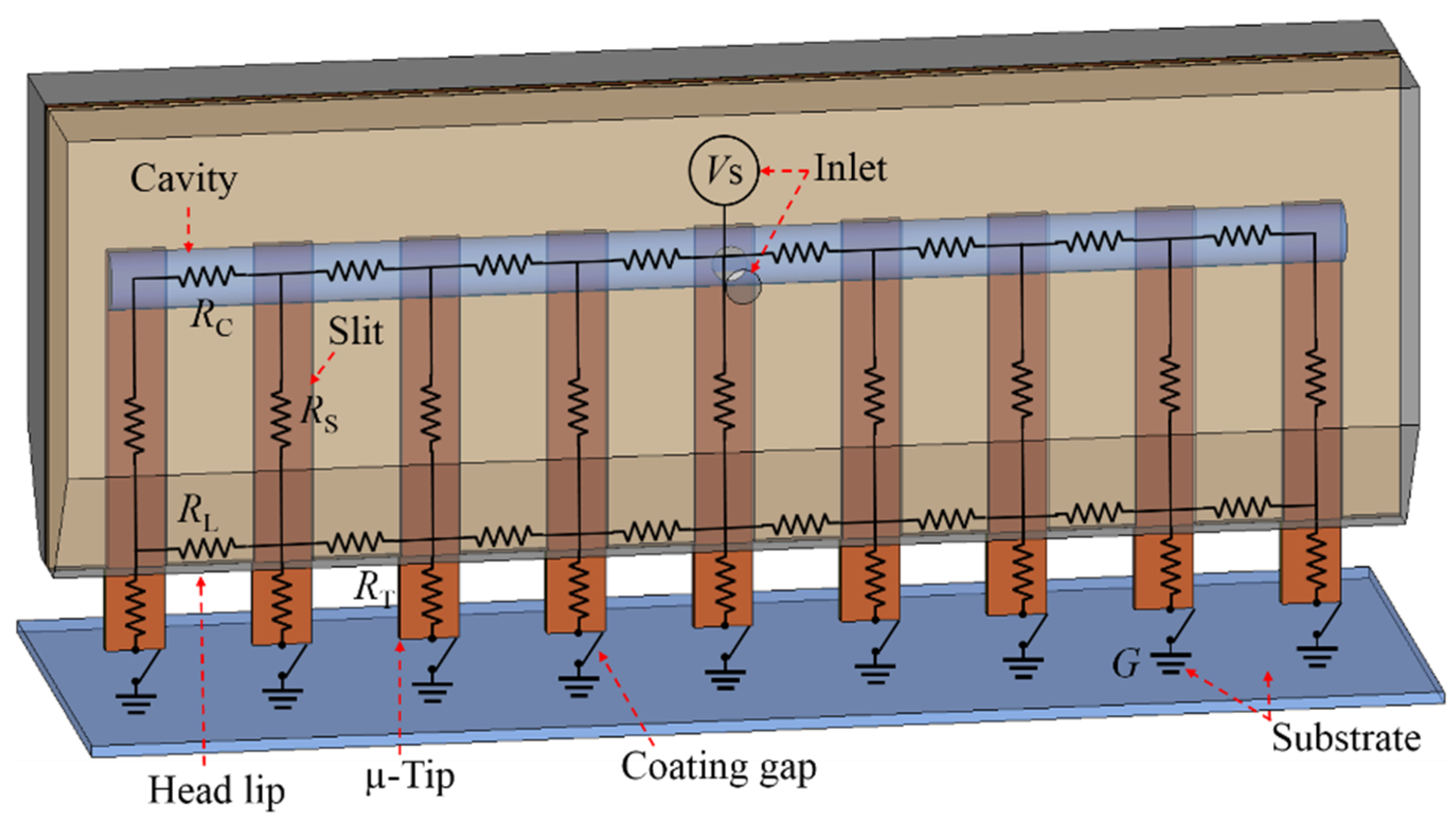
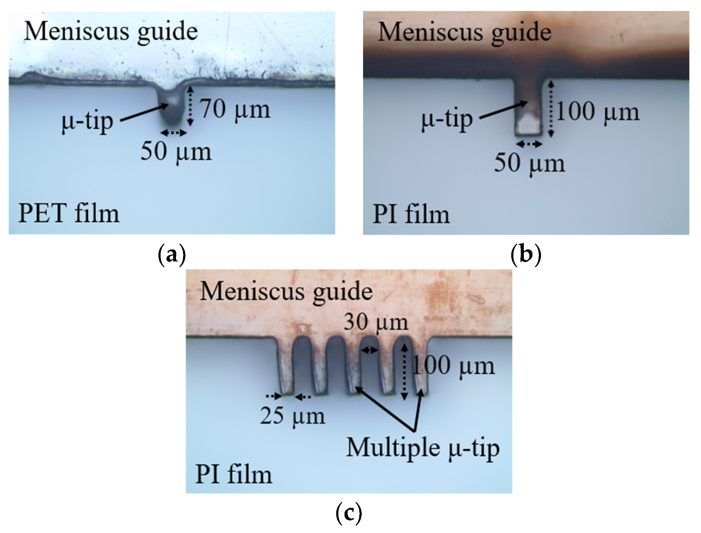
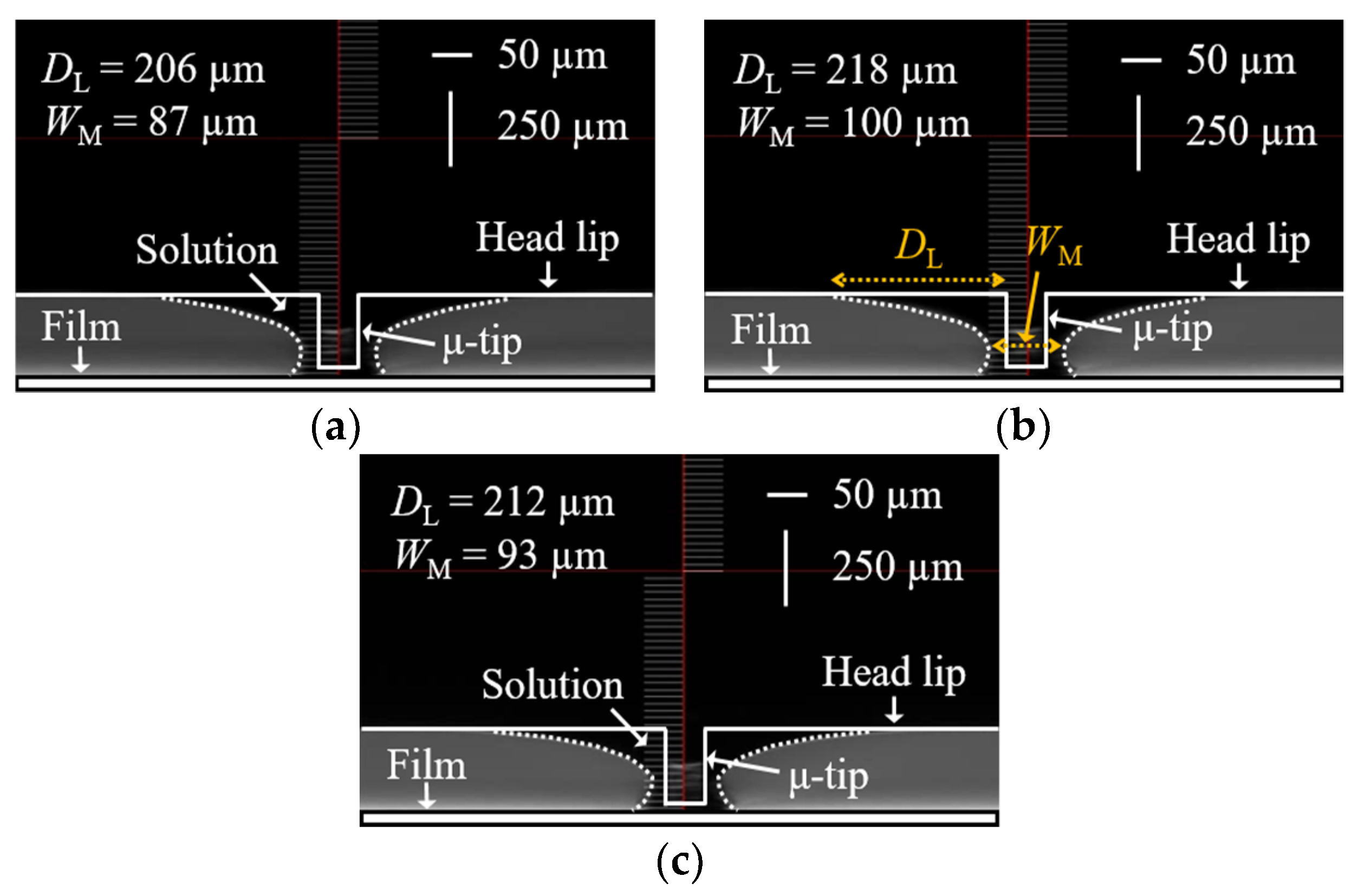
2.1. Simulation
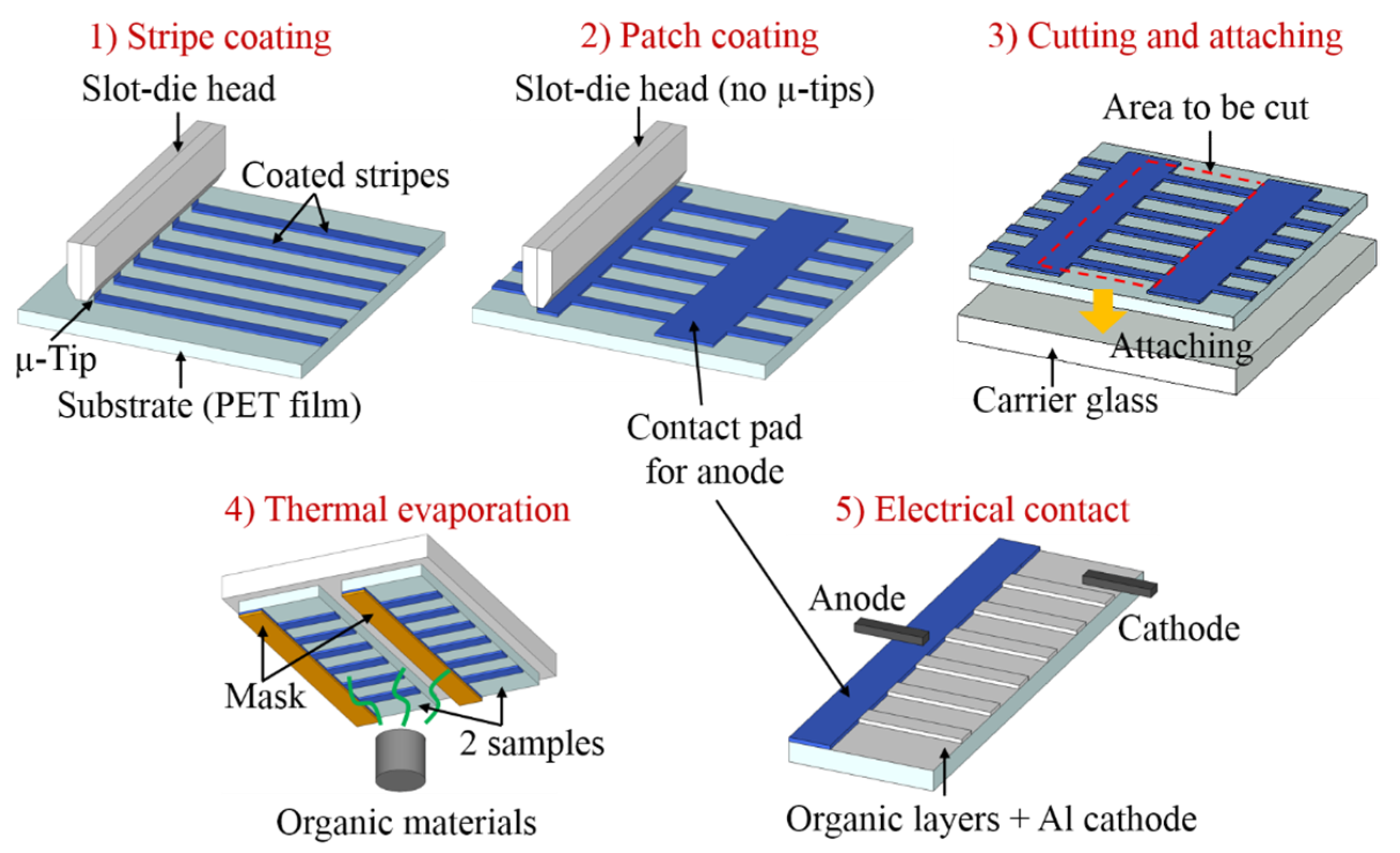
2.2. Experiment
3. Results and Discussion
3.1. Single Line Coating
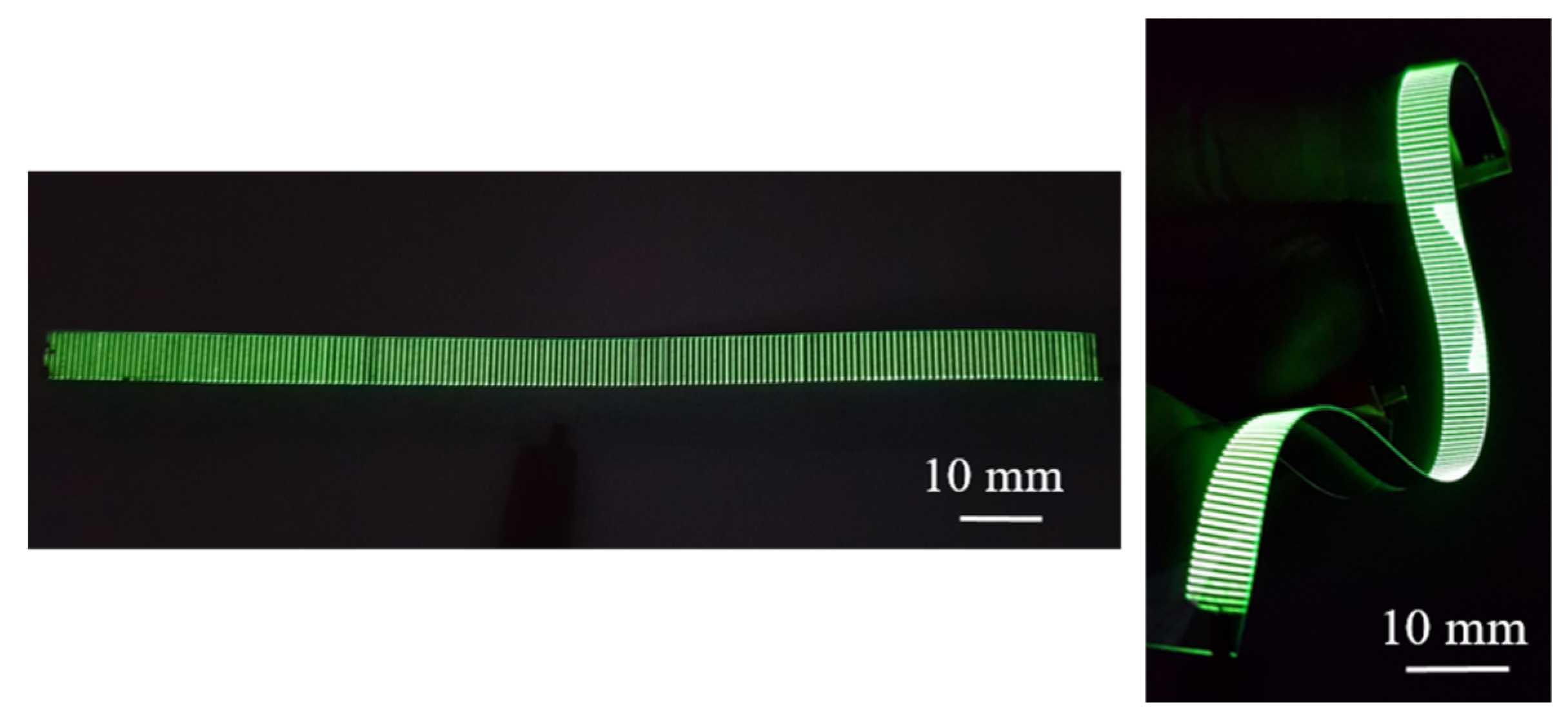
3.2. High-Density Line Coating
4. Conclusions
Author Contributions
Funding
Conflicts of Interest
References
- Zhou, L.; Yang, L.; Yu, M.; Jiang, Y.; Liu, C.; Lai, W.; Huang, W. Inkjet-printed small-molecule organic light-emitting diodes: Halogen-free inks, printing optimization, and large-area patterning. ACS Appl. Mater. Interfaces 2017, 9, 40533–40540. [Google Scholar] [CrossRef] [PubMed]
- Ha, T.W.; Kim, Y.B.; Heo, G.S.; Hwang, I.; Jeon, H.G.; Park, B. Organic light-emitting devices based on solution-processable small molecular emissive layers doped with interface-engineering additives. RSC Adv. 2016, 6, 33063. [Google Scholar] [CrossRef]
- Dubey, D.K.; Sahoo, S.; Wang, C.W.; Jou, J.-H. Solution process feasible highly efficient white organic light emitting diode. Org. Electron. 2019, 69, 232–240. [Google Scholar] [CrossRef]
- Chen, Y.; Wang, J.; Zhong, Z.; Jiang, Z.; Song, C.; Hu, Z.; Peng, J.; Wang, J.; Gao, Y. Fabricating large-area white OLED lighting panels via dip-coating. Org. Electron. 2016, 37, 458–464. [Google Scholar] [CrossRef]
- Morales-Masis, M.; Dauzou, F.; Jeangros, Q.; Dabirian, A.; Lifka, H.; Gierth, R.; Ruske, M.; Moet, D.; Hessler-Wyser, A.; Ballif, C. An indium-free anode for large-area flexible OLEDs: Defect-free transparent conductive zinc tin oxide. Adv. Funct. Mater. 2016, 26, 384–392. [Google Scholar] [CrossRef]
- Gu, X.; Zhou, Y.; Kevin, G.; Kurosawa, T.; Gun, Y.; Li, Y.; Lin, H.; Schroeder, B.C.; Yan, H.; Molina-Lopez, F.; et al. Roll-to-roll printed large-area all-polymer solar cells with 5% efficiency based on a low crystallinity conjugated polymer blend. Adv. Energy Mater. 2017, 7, 1602742. [Google Scholar] [CrossRef]
- Chern, Y.-C.; Wu, H.-R.; Chen, Y.-C.; Zan, H.-W.; Meng, H.-F.; Horng, S.-F. Reliable solution processed planar perovskite hybrid solar cells with large-area uniformity by chloroform soaking and spin rinsing induced surface precipitation. AIP Adv. 2015, 5, 087125. [Google Scholar] [CrossRef]
- Wang, T.; Zhang, Y.; Liu, Q.; Cheng, W.; Wang, X.; Pan, L.; Xu, B.; Xu, H. A self-healable, highly stretchable, and solution processable conductive polymer composite for ultrasensitive strain and pressure sensing. Adv. Funct. Mater. 2018, 28, 1705551. [Google Scholar] [CrossRef]
- Khim, D.; Ryu, G.S.; Park, W.T.; Kim, H.; Lee, M.; Noh, Y. Precisely controlled ultrathin conjugated polymer films for large area transparent transistors and highly sensitive chemical sensors. Adv. Mater. 2016, 28, 2752–2759. [Google Scholar] [CrossRef]
- Liu, Y.; Elzatahry, A.A.; Luo, W.; Lan, K.; Zhang, P.; Fan, J.; Wei, Y.; Wang, C.; Deng, Y.; Zheng, G.; et al. Surfactant-templating strategy for ultrathin mesoporous TiO2 coating on flexible graphitized carbon supports for high-performance lithium-ion battery. Nano Energy 2016, 25, 80–90. [Google Scholar] [CrossRef]
- He, J.; Bao, K.; Cui, W.; Yu, J.; Huang, C.; Shen, X.; Cui, Z.; Wang, N. Construction of large-area uniform graphdiyne film for high-performance lithium-ion batteries. Chem. Eur. J. 2018, 24, 1187–1192. [Google Scholar] [CrossRef] [PubMed]
- Zheng, X.; Liu, Y.; Zhu, Y.; Ma, F.; Feng, C.; Yu, Y.; Hu, H.; Li, F. Efficient inkjet-printed blue OLED with boosted charge transport using host doping for application in pixelated display. Opt. Mater. 2020, 101, 109755. [Google Scholar] [CrossRef]
- Hu, Z.; Yin, Y.; Ali, M.U.; Peng, W.; Zhang, S.; Li, D.; Zou, T.; Li, Y.; Jiao, S.; Chen, S.; et al. Inkjet printed uniform quantum dots as color conversion layers for full-color OLED displays. Nanoscale 2020, 12, 2103–2110. [Google Scholar] [CrossRef]
- Merklein, L.; Daume, D.; Braig, F.; Schlisske, S.; Rödlmeier, T.; Mink, M.; Kourkoulos, D.; Ulber, B.; Biase, M.D.; Meerholz, K.; et al. Comparative study of printed multilayer OLED fabrication through slot die coating, gravure and inkjet printing, and their combination. Colloids Interfaces 2019, 3, 32. [Google Scholar] [CrossRef]
- Smarsly, E.; Daume, D.; Tone, R.; Veith, L.; Curticean, E.R.; Wacker, I.; Schröder, R.R.; Sauer, H.M.; Dörsam, E.; Bunz, U.H.F. Printing poly (p-phenyleneethynylene) PLEDs. ACS Appl. Mater. Interfaces 2019, 11, 3317–3322. [Google Scholar] [CrossRef] [PubMed]
- Lee, Y.G.; Lee, D.J.; Bae, J.H.; Lee, J.Y.; Jung, B.J.; Lee, J. Investigation of nozzle printing parameters for OLED emitting layers. Mol. Cryst. Liq. Cryst. 2018, 660, 17–23. [Google Scholar] [CrossRef]
- Yoon, D.G.; Kang, M.G.; Kim, J.B.; Kang, K. Nozzle printed-PEDOT: PSS for organic light emitting diodes with various dilution rates of ethanol. Appl. Sci. 2018, 8, 203. [Google Scholar] [CrossRef]
- Staat, H.J.; van der Bos, A.; van den Berg, M.; Reinten, H.; Wijshoff, H.; Versluis, M.; Lohse, D. Ultrafast imaging method to measure surface tension and viscosity of inkjet-printed droplets in flight. Exp. Fluids 2017, 58, 2. [Google Scholar] [CrossRef]
- Razza, S.; Di Giacomo, F.; Matteocci, F.; CinÓ, L.; Palma, A.L.; Casaluci, S.; Cameron, P.; D’Epifanio, A.; Licoccia, S.; Reale, A.; et al. Perovskite solar cells and large area modules (100 cm2) based on an air flow-assisted PbI2 blade coating deposition process. J. Power Sources 2015, 277, 286–291. [Google Scholar] [CrossRef]
- Seok, J.Y.; Yang, M. A novel blade-jet coating method for achieving ultrathin, uniform film toward all-solution-processed large-area organic light-emitting diodes. Adv. Mater. Technol. 2016, 1, 1600029. [Google Scholar] [CrossRef]
- Cang, Y.-F.; Yang, L.-S.; Su, H.-T.; Liao, S.-Y.; Niu, M.-C.; Mahesh, K.P.O.; Chen, C.-H.; Chao, Y.-C.; Meng, H.-F.M.; Huang, H.-L.; et al. All-solution-processed red and orange-red organic light-emitting diodes with high-efficiencies: The effect of mixed-host emissive layers and thermal annealing treatment. ChemPlusChem 2019, 84, 1375–1383. [Google Scholar] [CrossRef]
- Park, B.; Kwon, O.E.; Yun, S.H.; Jeon, H.G.; Huh, Y.H. Organic semiconducting layers fabricated by selfmetered slot-die coating for solution-processable organic light-emitting devices. J. Mater. Chem. C 2014, 2, 8614–8621. [Google Scholar] [CrossRef]
- Griffin, J.; Ryan, A.J.; Lidzey, D.G. Solution modification of PEDOT: PSS inks for ultrasonic spray coating. Org. Electron. 2017, 41, 245–250. [Google Scholar] [CrossRef]
- Koutsiaki, C.; Kaimakamis, T.; Zachariadis, A.; Papamichail, A.; Kamaraki, C.; Fachouri, S.; Gravalids, C.; Laskarakis, A.; Logothetidis, S. Efficient combination of roll-to-roll compatible techniques towards the large area deposition of a polymer dielectric film and the solution-processing of an organic semiconductor for the field-effect transistors fabrication on plastic substrate. Org. Electron. 2019, 73, 231–239. [Google Scholar] [CrossRef]
- Han, D.; Yasser, K.; Karthik, G.; Adrien, P.; Ana, C.A. Emission area patterning of organic light-emitting diodes (OLEDs) via printed dielectrics. Adv. Funct. Mater. 2018, 28, 1802986. [Google Scholar] [CrossRef]
- Mohamad, D.K.; Griffin, J.; Bracher, C.; Barrows, A.T.; Lidzey, D.G. Spray-cast multilayer organometal perovskite solar cells fabricated in air. Adv. Energy Mater. 2016, 6, 1600994. [Google Scholar] [CrossRef]
- Lin, C.F.; Wong, D.S.; Liu, T.; Wu, P. Operating windows of slot die coating: Comparison of theoretical predictions with experimental observations. Adv. Polym. Technol. 2010, 29, 31–44. [Google Scholar] [CrossRef]
- Carvalho, M.S.; Kheshgi, H.S. Low-flow limit in slot coating: Theory and experiments. AlChE J. 2000, 46, 1907–1917. [Google Scholar] [CrossRef]
- Larsen-Olsen, T.T.; Andreasen, B.; Andersen, T.R.; Böttiger, A.P.L.; Bundgaard, E.; Norrman, K.; Andreasen, J.W.; Jørgensen, M.; Krebs, F.C. Simultaneous multilayer formation of the polymer solar cell stack using roll-to-roll double slot-die coating from water. Sol. Energy Mater. Sol. Cells 2012, 97, 22–27. [Google Scholar] [CrossRef]
- Kang, H.; Park, J.; Shin, K. Statistic analysis for the manufacturing of multi-strip patterns by roll-to-roll single slot-die systems. Robot. Comput. Integr. Manuf. 2014, 30, 363–368. [Google Scholar] [CrossRef]
- Abbel, R.; de Vries, I.; Langen, A.; Kirchner, G.; t’Mnnetje, H.; Gorter, H.; Wilson, J. Toward high volume solution based roll-to-roll processing of OLEDs. J. Mater. Res. 2017, 32, 2219–2229. [Google Scholar] [CrossRef]
- Liu, H.; Xu, W.; Tan, W.; Zhu, X.; Wang, J.; Peng, J.; Cao, Y. Line printing solution-processable small molecules with uniform surface profile via ink-jet printer. J. Colloid Interface Sci. 2016, 465, 106–111. [Google Scholar] [CrossRef] [PubMed]
- Singh, M.; Haverinen, H.M.; Dhagat, P.; Jabbour, G.E. Inkjet printing-process and its applications. Adv. Mater. 2010, 22, 673–685. [Google Scholar] [CrossRef] [PubMed]
- Soltman, D.; Subramanian, V. Inkjet-printed line morphologies and temperature control of the coffee ring effect. Langmuir 2008, 24, 2224–2231. [Google Scholar] [CrossRef]
- Han, D.H.; Lee, S.H.; Ahn, W.; Nam, J.; Jung, H.W. Effect of shim configuration on flow dynamics and operability windows in stripe slot coating process. J. Coat. Technol. Res. 2014, 11, 19–29. [Google Scholar] [CrossRef]
- Krebs, F.C. Polymer solar cell modules prepared using roll-to-roll methods: Knife-over-edge coating, slot-die coating and screen printing. Sol. Energy Mater. Sol. Cells 2009, 93, 465–475. [Google Scholar] [CrossRef]
- Liu, K.; Larsen-Olsen, T.T.; Lin, Y.; Beliatis, M.; Bundgaard, E.; Jørgensen, M.; Krebs, F.C.; Zhan, X. Roll-coating fabrication of flexible organic solar cells: Comparison of fullerene and fullerene-free systems. J. Mater. Chem. A 2016, 4, 1044–1051. [Google Scholar] [CrossRef]
- Verma, A.; Martineau, D.; Hack, E.; Makha, M.; Turner, E.; Nüesch, F.; Heier, J. Towards industrialization of perovskite solar cells using slot die coating. J. Mater. Chem. C 2020, 8, 6124–6135. [Google Scholar] [CrossRef]
- Kim, G.; Lee, J.; Shin, D.; Park, J. Roll-to-roll fabrication of PEDOT: PSS Stripes using slot-die head with μ-tips for AMOLEDs. IEEE Trans. Electron. Devices 2019, 66, 1041–1049. [Google Scholar] [CrossRef]
- Kim, G.E.; Shin, D.K.; Lee, J.Y.; Park, J.W. Effect of surface morphology of slot-die heads on roll-to-roll coatings of fine PEDOT: PSS stripes. Org. Electron. 2019, 66, 116–125. [Google Scholar] [CrossRef]
- Lee, J.; Park, J. Increased stripe density of slot-coated PEDOT: PSS using a meniscus guide with linearly tapered μ-tips for OLEDs. Org. Electron. 2020, 83, 105772. [Google Scholar] [CrossRef]
- Lun, I.; Calay, R.K.; Holdo, A.E. Modelling two-phase flows using CFD. Appl. Energy 1996, 53, 299–314. [Google Scholar] [CrossRef]
- Sartor, L. Slot Coating: Fluid Mechanics and Die Design. Ph.D. Thesis, University of Minnesota, Saint Paul, MN, USA, 1990. [Google Scholar]
- Bhamidipati, K.L.; Didari, S.; Bedell, P.; Harris, T.A.L. Wtting phenomena during processing of high-viscosity shear-thinning fluid. J. Non Newton. Fluid Mech. 2011, 166, 723–733. [Google Scholar] [CrossRef]
- Bhamidipati, K.L.; Didari, S.; Harris, T.A.L. Experimental study on air entrainment in slot die coating of high-viscosity, shear-thinning solutions. Chem. Eng. Sci. 2012, 80, 195–204. [Google Scholar] [CrossRef]
- Nam, J.; Scriven, L.E.; Carvalho, M.S. Tracking birth of vortex in flows. J. Comput. Phys. 2009, 228, 4549–4567. [Google Scholar] [CrossRef]
- Oh, K.W.; Lee, K.; Ahn, B.; Furlani, E.P. Design of pressure-driven microfluidic networks using electric circuit analogy. Lab Chip 2012, 12, 515–545. [Google Scholar] [CrossRef]
- Lee, K.; Kim, C.; Ahn, B.; Panchapakesan, R.; Full, A.R.; Nordee, L.; Kang, J.Y.; Oh, K.W. Generalized serial dilution module for monotonic and arbitrary microfluidic gradient generators. Lab Chip 2009, 9, 709–717. [Google Scholar] [CrossRef]
- Ahmad, N.A.; Bahry, S.I.S.; Ali, Z.M.; Daud, A.M.M.; Musa, S. Effect of flow resistance in open rectangular channel. MATEC Web Conf. 2017, 97, 01107. [Google Scholar] [CrossRef]
- Angelescu, D.E. Highly Integrated Microfluidics Design; Artech House: Boston, MA, USA, 2011. [Google Scholar]
- Mortensen, N.A.; Okkels, F.; Bruus, H. Reexamination of Hagen-Poiseuille flow: Shape dependence of the hydraulic resistance in microchannels. Phys. Rev. E 2005, 71, 057301. [Google Scholar] [CrossRef]


| Coating Speed | 50-µm-Wide Slit Channel | 150-µm-Wide Slit Channel | Reversely Tapered Slit Channel | |||
|---|---|---|---|---|---|---|
| V (mm/s) | W (µm) | T (nm) | W (µm) | T (nm) | W (µm) | T (nm) |
| 10 | 131 ± 2 | 113 ± 3 | 151 ± 2 | 139 ± 3 | 145 ± 2 | 131 ± 4 |
| 13 | 112 ± 2 | 105 ± 2 | 130 ± 1 | 130 ± 2 | 126 ± 2 | 124 ± 2 |
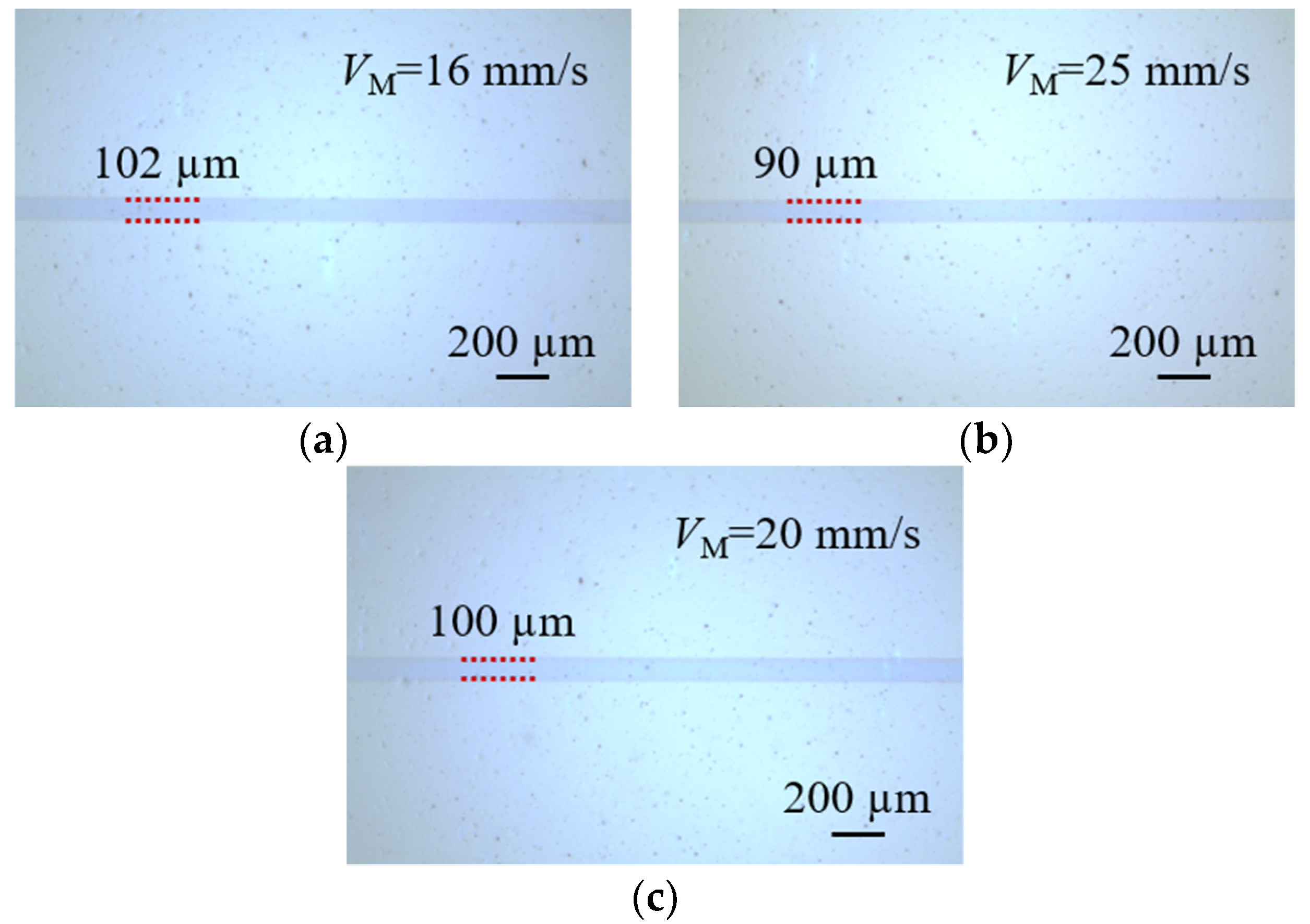
| 16 | 102 ± 2 | 90 ± 2 | 117 ± 2 | 125 ± 3 | 112 ± 1 | 118 ± 2 |
| 20 | Line breakup | 103 ± 2 | 118 ± 3 | 100 ± 2 | 108 ± 5 | |
| 25 | 90 ± 2 | 105 ± 4 | Line breakup | |||
© 2020 by the authors. Licensee MDPI, Basel, Switzerland. This article is an open access article distributed under the terms and conditions of the Creative Commons Attribution (CC BY) license (http://creativecommons.org/licenses/by/4.0/).
Share and Cite
Shin, D.; Lee, J.; Park, J. Effect of Slit Channel Width of a Shim Embedded in Slot-Die Head on High-Density Stripe Coating for OLEDs. Coatings 2020, 10, 772. https://doi.org/10.3390/coatings10080772
Shin D, Lee J, Park J. Effect of Slit Channel Width of a Shim Embedded in Slot-Die Head on High-Density Stripe Coating for OLEDs. Coatings. 2020; 10(8):772. https://doi.org/10.3390/coatings10080772
Chicago/Turabian StyleShin, Dongkyun, Jinyoung Lee, and Jongwoon Park. 2020. "Effect of Slit Channel Width of a Shim Embedded in Slot-Die Head on High-Density Stripe Coating for OLEDs" Coatings 10, no. 8: 772. https://doi.org/10.3390/coatings10080772
APA StyleShin, D., Lee, J., & Park, J. (2020). Effect of Slit Channel Width of a Shim Embedded in Slot-Die Head on High-Density Stripe Coating for OLEDs. Coatings, 10(8), 772. https://doi.org/10.3390/coatings10080772