
The Effect of Trap Design on the Scalability of Trapped-Ion Quantum Technologies


Abstract
1. Introduction
2. Field Characterization
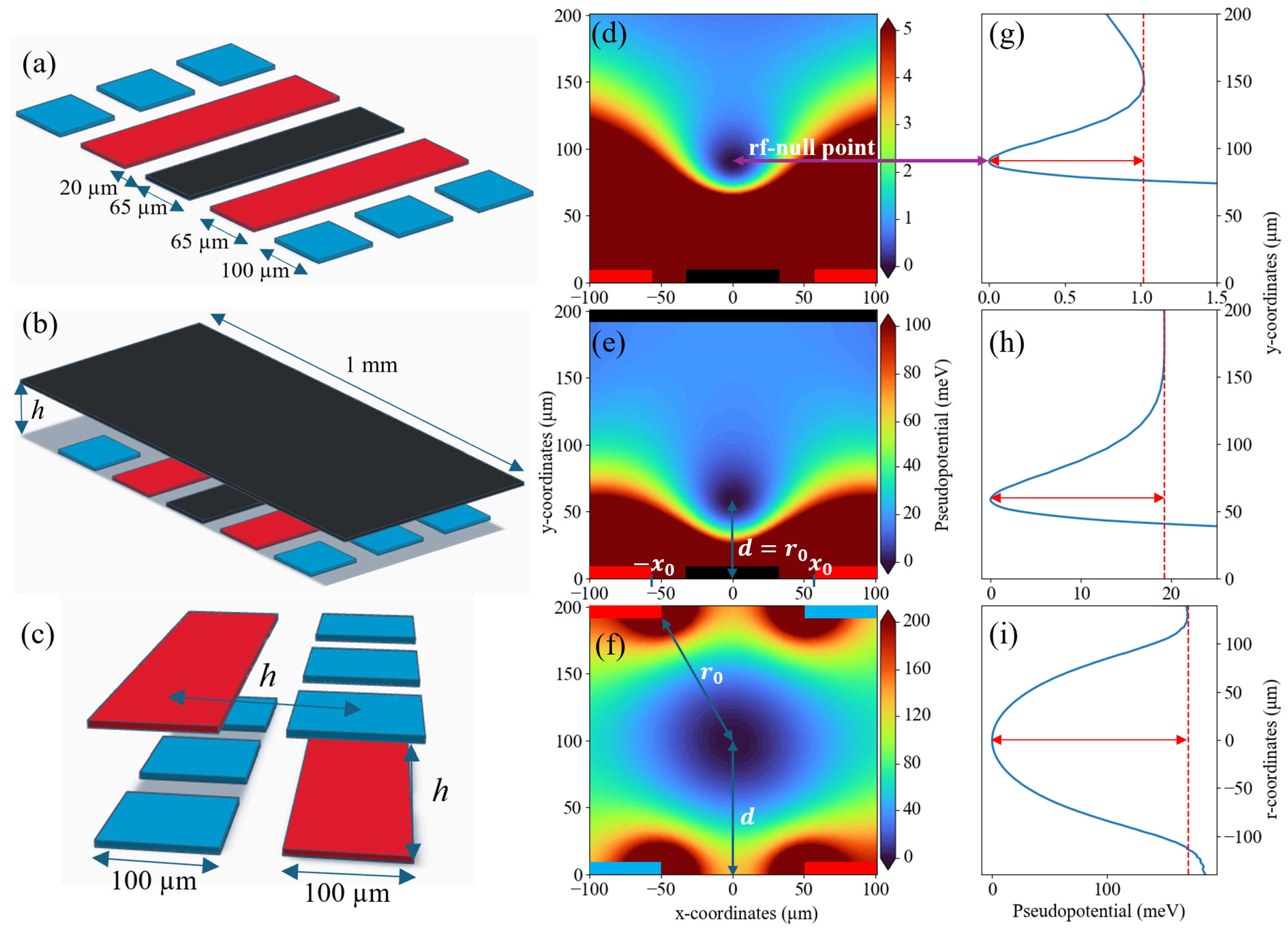
2.1. Calculation of Trapping Potential
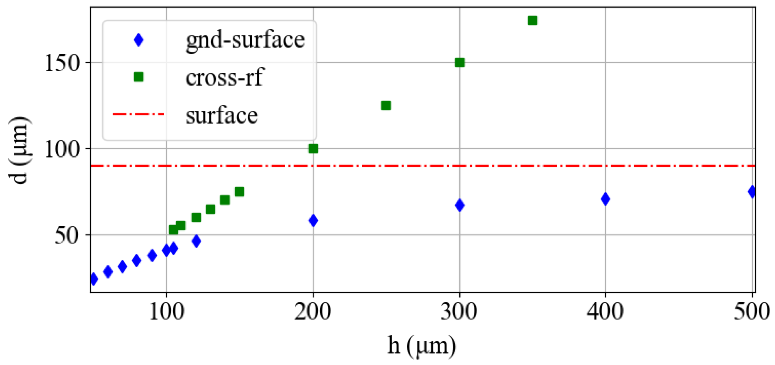
2.2. Ion Height
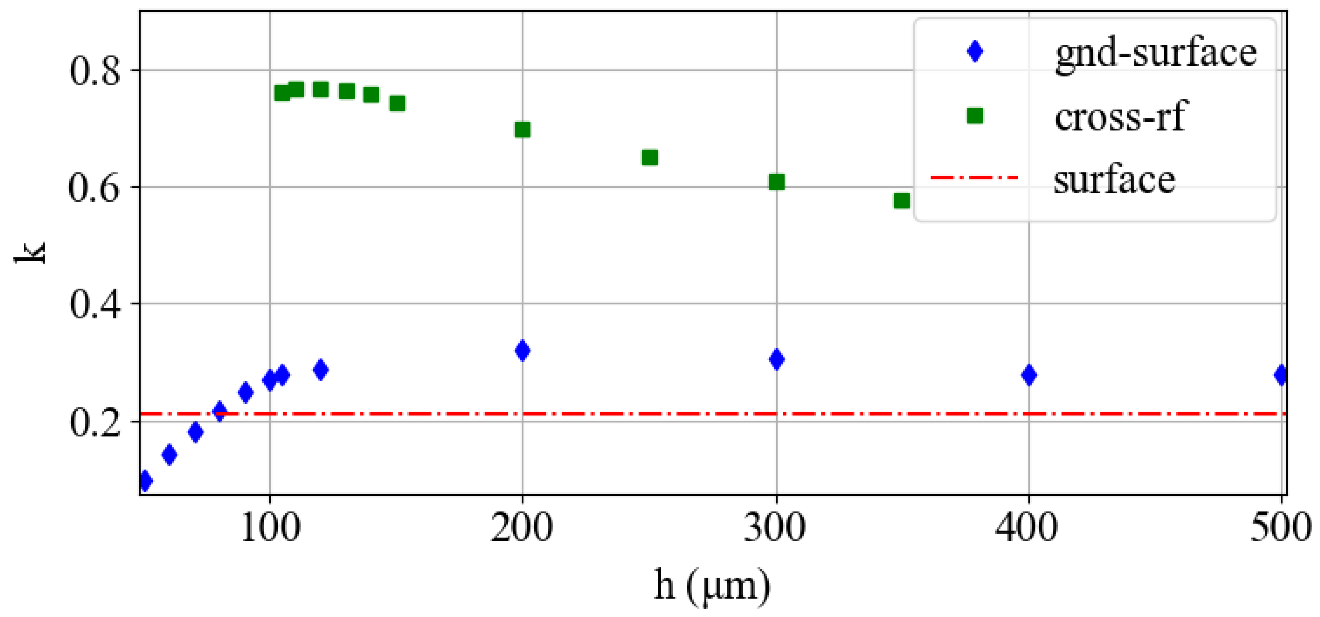
2.3. Harmonicity
2.4. Trap Depth
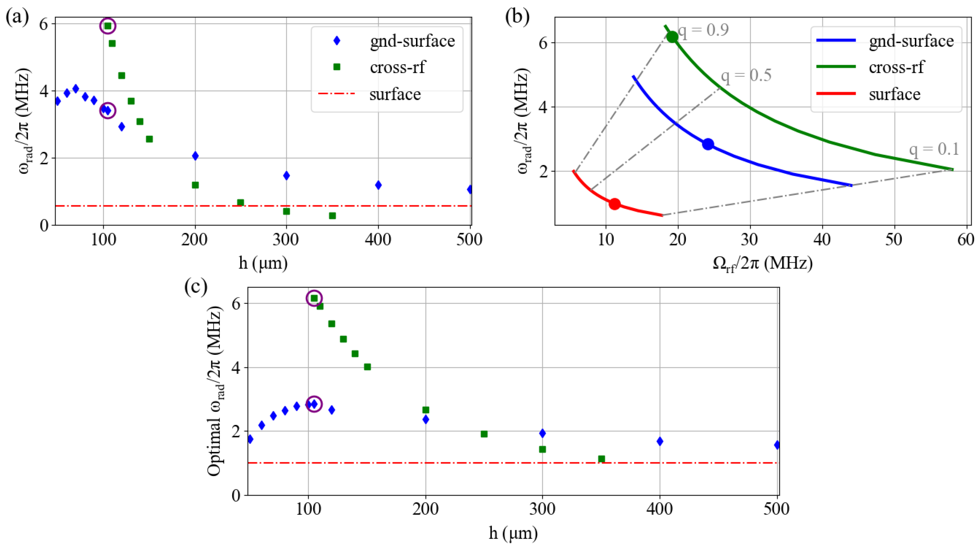
2.5. Trap Frequency
3. Expected Experimental Performance
3.1. Heating Rate
3.2. Achieving a Target Trap Frequency
4. Practicality
4.1. Fabrication
4.2. Optical Access
5. Conclusions and Outlook
Author Contributions
Funding
Data Availability Statement
Acknowledgments
Conflicts of Interest
References
- Ludlow, A.D.; Boyd, M.M.; Ye, J.; Peik, E.; Schmidt, P.O. Optical atomic clocks. Rev. Mod. Phys. 2015, 87, 637–701. [Google Scholar] [CrossRef]
- Gilmore, K.A.; Affolter, M.; Lewis-Swan, R.J.; Barberena, D.; Jordan, E.; Rey, A.M.; Bollinger, J.J. Quantum-enhanced sensing of displacements and electric fields with two-dimensional trapped-ion crystals. Science 2021, 373, 673–678. [Google Scholar] [CrossRef]
- Blatt, R.; Roos, C.F. Quantum simulations with trapped ions. Nat. Phys. 2012, 8, 277–284. [Google Scholar] [CrossRef]
- Wineland, D.J.; Barrett, M.; Britton, J.; Chiaverini, J.; DeMarco, B.; Itano, W.M.; Jelenković, B.; Langer, C.; Leibfried, D.; Meyer, V.; et al. Quantum information processing with trapped ions. Philos. Trans. R. Soc. London. Ser. Math. Phys. Eng. Sci. 2003, 361, 1349–1361. [Google Scholar] [CrossRef] [PubMed]
- Schindler, P.; Nigg, D.; Monz, T.; Barreiro, J.T.; Martinez, E.; Wang, S.X.; Quint, S.; Brandl, M.F.; Nebendahl, V.; Roos, C.F.; et al. A quantum information processor with trapped ions. New J. Phys. 2013, 15, 123012. [Google Scholar] [CrossRef]
- An, F.A.; Ransford, A.; Schaffer, A.; Sletten, L.R.; Gaebler, J.; Hostetter, J.; Vittorini, G. High Fidelity State Preparation and Measurement of Ion Hyperfine Qubits with I 1/2. Phys. Rev. Lett. 2022, 129, 130501. [Google Scholar] [CrossRef]
- Ballance, C.J.; Harty, T.P.; Linke, N.M.; Sepiol, M.A.; Lucas, D.M. High-Fidelity Quantum Logic Gates Using Trapped-Ion Hyperfine Qubits. Phys. Rev. Lett. 2016, 117, 060504. [Google Scholar] [CrossRef]
- Clark, C.R.; Tinkey, H.N.; Sawyer, B.C.; Meier, A.M.; Burkhardt, K.A.; Seck, C.M.; Shappert, C.M.; Guise, N.D.; Volin, C.E.; Fallek, S.D.; et al. High-Fidelity Bell-State Preparation with 40Ca+ Optical Qubits. Phys. Rev. Lett. 2021, 127, 130505. [Google Scholar] [CrossRef]
- Sawyer, B.C.; Brown, K.R. Wavelength-insensitive, multispecies entangling gate for group-2 atomic ions. Phys. Rev. A 2021, 103, 022427. [Google Scholar] [CrossRef]
- Ospelkaus, C.; Warring, U.; Colombe, Y.; Brown, K.R.; Amini, J.M.; Leibfried, D.; Wineland, D.J. Microwave quantum logic gates for trapped ions. Nature 2011, 476, 181–184. [Google Scholar] [CrossRef]
- Weber, M.A.; Gely, M.F.; Hanley, R.K.; Harty, T.P.; Leu, A.D.; Löschnauer, C.M.; Nadlinger, D.P.; Lucas, D.M. Robust and fast microwave-driven quantum logic for trapped-ion qubits. Phys. Rev. A 2024, 110, L010601. [Google Scholar] [CrossRef]
- Löschnauer, C.M.; Toba, J.M.; Hughes, A.C.; King, S.A.; Weber, M.A.; Srinivas, R.; Matt, R.; Nourshargh, R.; Allcock, D.T.C.; Ballance, C.J.; et al. Scalable, high-fidelity all-electronic control of trapped-ion qubits. arXiv 2024, arXiv:2407.07694. [Google Scholar] [CrossRef]
- Paul, W. Electromagnetic traps for charged and neutral particles. Rev. Mod. Phys. 1990, 62, 531–540. [Google Scholar] [CrossRef]
- Chiaverini, J.; Blakestad, R.B.; Britton, J.; Jost, J.D.; Langer, C.; Leibfried, D.; Ozeri, R.; Wineland, D.J. Surface-electrode architecture for ion-trap quantum information processing. Quantum Inf. Comput. 2005, 5, 419–439. [Google Scholar] [CrossRef]
- Zhang, J.; Pagano, G.; Hess, P.W.; Kyprianidis, A.; Becker, P.; Kaplan, H.; Gorshkov, A.V.; Gong, Z.X.; Monroe, C. Observation of a many-body dynamical phase transition with a 53-qubit quantum simulator. Nature 2017, 551, 601–604. [Google Scholar] [CrossRef]
- Pino, J.M.; Dreiling, J.M.; Figgatt, C.; Gaebler, J.P.; Moses, S.A.; Allman, M.S.; Baldwin, C.H.; Foss-Feig, M.; Hayes, D.; Mayer, K.; et al. Demonstration of the trapped-ion quantum CCD computer architecture. Nature 2021, 592, 209–213. [Google Scholar] [CrossRef]
- Pogorelov, I.; Feldker, T.; Marciniak, C.D.; Postler, L.; Jacob, G.; Krieglsteiner, O.; Podlesnic, V.; Meth, M.; Negnevitsky, V.; Stadler, M.; et al. Compact Ion-Trap Quantum Computing Demonstrator. PRX Quantum 2021, 2, 020343. [Google Scholar] [CrossRef]
- Moses, S.; Baldwin, C.; Allman, M.; Ancona, R.; Ascarrunz, L.; Barnes, C.; Bartolotta, J.; Bjork, B.; Blanchard, P.; Bohn, M.; et al. A Race-Track Trapped-Ion Quantum Processor. Phys. Rev. X 2023, 13, 041052. [Google Scholar] [CrossRef]
- Chen, J.S.; Nielsen, E.; Ebert, M.; Inlek, V.; Wright, K.; Chaplin, V.; Maksymov, A.; Páez, E.; Poudel, A.; Maunz, P.; et al. Benchmarking a trapped-ion quantum computer with 30 qubits. Quantum 2024, 8, 1516. [Google Scholar] [CrossRef]
- Postler, L.; Butt, F.; Pogorelov, I.; Marciniak, C.D.; Heußen, S.; Blatt, R.; Schindler, P.; Rispler, M.; Müller, M.; Monz, T. Demonstration of Fault-Tolerant Steane Quantum Error Correction. PRX Quantum 2024, 5, 030326. [Google Scholar] [CrossRef]
- Reichardt, B.W.; Aasen, D.; Chao, R.; Chernoguzov, A.; van Dam, W.; Gaebler, J.P.; Gresh, D.; Lucchetti, D.; Mills, M.; Moses, S.A.; et al. Demonstration of quantum computation and error correction with a tesseract code. arXiv 2024, arXiv:2409.04628. [Google Scholar] [CrossRef]
- Zhang, C.; Pokorny, F.; Li, W.; Higgins, G.; Pöschl, A.; Lesanovsky, I.; Hennrich, M. Submicrosecond entangling gate between trapped ions via Rydberg interaction. Nature 2020, 580, 345–349. [Google Scholar] [CrossRef] [PubMed]
- Saha, S.; Shalaev, M.; O’Reilly, J.; Goetting, I.; Toh, G.; Kalakuntla, A.; Yu, Y.; Monroe, C. High-fidelity remote entanglement of trapped atoms mediated by time-bin photons. Nat. Commun. 2025, 16, 2533. [Google Scholar] [CrossRef]
- Saner, S.; Băzăvan, O.; Minder, M.; Drmota, P.; Webb, D.J.; Araneda, G.; Srinivas, R.; Lucas, D.M.; Ballance, C.J. Breaking the Entangling Gate Speed Limit for Trapped-Ion Qubits Using a Phase-Stable Standing Wave. Phys. Rev. Lett. 2023, 131, 220601. [Google Scholar] [CrossRef]
- Schäfer, V.M.; Ballance, C.J.; Thirumalai, K.; Stephenson, L.J.; Ballance, T.G.; Steane, A.M.; Lucas, D.M. Fast quantum logic gates with trapped-ion qubits. Nature 2018, 555, 75–78. [Google Scholar] [CrossRef] [PubMed]
- Steane, A.; Roos, C.F.; Stevens, D.; Mundt, A.; Leibfried, D.; Schmidt-Kaler, F.; Blatt, R. Speed of ion-trap quantum-information processors. Phys. Rev. A 2000, 62, 042305. [Google Scholar] [CrossRef]
- Brownnutt, M.; Kumph, M.; Rabl, P.; Blatt, R. Ion-trap measurements of electric-field noise near surfaces. Rev. Mod. Phys. 2015, 87, 1419–1482. [Google Scholar] [CrossRef]
- Ghosh, P.K. Ion Traps; A Clarendon Press Publication: Oxford, UK, 1995. [Google Scholar]
- Kajita, M. Ion Traps; IOP Publishing: Bristol, UK, 2022; pp. 2053–2563. [Google Scholar] [CrossRef]
- Pearson, C.E.; Leibrandt, D.R.; Bakr, W.S.; Mallard, W.J.; Brown, K.R.; Chuang, I.L. Experimental investigation of planar ion traps. Phys. Rev. A 2006, 73, 032307. [Google Scholar] [CrossRef]
- Allcock, D.T.C.; Sherman, J.A.; Stacey, D.N.; Burrell, A.H.; Curtis, M.J.; Imreh, G.; Linke, N.M.; Szwer, D.J.; Webster, S.C.; Steane, A.M.; et al. Implementation of a symmetric surface-electrode ion trap with field compensation using a modulated Raman effect. New J. Phys. 2010, 12, 053026. [Google Scholar] [CrossRef]
- Hong, S.; Lee, M.; Cheon, H.; Kim, T.; Cho, D.-i. Guidelines for Designing Surface Ion Traps Using the Boundary Element Method. Sensors 2016, 16, 616. [Google Scholar] [CrossRef]
- Doret, S.C.; Amini, J.M.; Wright, K.; Volin, C.; Killian, T.; Ozakin, A.; Denison, D.; Hayden, H.; Pai, C.S.; Slusher, R.E.; et al. Controlling trapping potentials and stray electric fields in a microfabricated ion trap through design and compensation. New J. Phys. 2012, 14, 073012. [Google Scholar] [CrossRef]
- Moehring, D.L.; Highstrete, C.; Stick, D.; Fortier, K.M.; Haltli, R.; Tigges, C.; Blain, M.G. Design, fabrication and experimental demonstration of junction surface ion traps. New J. Phys. 2011, 13, 075018. [Google Scholar] [CrossRef]
- Wright, K.; Amini, J.M.; Faircloth, D.L.; Volin, C.; Doret, S.C.; Hayden, H.; Pai, C.S.; Landgren, D.W.; Denison, D.; Killian, T.; et al. Reliable transport through a microfabricated X-junction surface-electrode ion trap. New J. Phys. 2013, 15, 033004. [Google Scholar] [CrossRef]
- Mehta, K.K.; Bruzewicz, C.D.; McConnell, R.; Ram, R.J.; Sage, J.M.; Chiaverini, J. Integrated optical addressing of an ion qubit. Nat. Nanotechnol. 2016, 11, 1066–1070. [Google Scholar] [CrossRef]
- Maunz, P.L.W. High Optical Access Trap 2.0.; Technical Report; Sandia National Lab. (SNL-NM): Albuquerque, NM, USA, 2016. [Google Scholar] [CrossRef]
- Gerasin, I.; Zhadnov, N.; Kudeyarov, K.; Khabarova, K.; Kolachevsky, N.; Semerikov, I. Optimized Surface Ion Trap Design for Tight Confinement and Separation of Ion Chains. Quantum Rep. 2024, 6, 442–451. [Google Scholar] [CrossRef]
- Marquet, C.; Schmidt-Kaler, F.; James, D. Phonon-phonon interactions due to non-linear effects in a linear ion trap. Appl. Phys. B Lasers Opt. 2003, 76, 199–208. [Google Scholar] [CrossRef]
- Home, J.P.; Hanneke, D.; Jost, J.D.; Leibfried, D.; Wineland, D.J. Normal modes of trapped ions in the presence of anharmonic trap potentials. New J. Phys. 2011, 13, 073026. [Google Scholar] [CrossRef]
- Wu, Y.; Wang, S.T.; Duan, L.M. Noise analysis for high-fidelity quantum entangling gates in an anharmonic linear Paul trap. Phys. Rev. A 2018, 97, 062325. [Google Scholar] [CrossRef]
- Alheit, R.; Chu, X.Z.; Hoefer, M.; Holzki, M.; Werth, G.; Blümel, R. Nonlinear collective oscillations of an ion cloud in a Paul trap. Phys. Rev. A 1997, 56, 4023–4031. [Google Scholar] [CrossRef]
- Razvi, M.A.N.; Chu, X.Z.; Alheit, R.; Werth, G.; Blümel, R. Fractional frequency collective parametric resonances of an ion cloud in a Paul trap. Phys. Rev. A 1998, 58, R34–R37. [Google Scholar] [CrossRef]
- Drakoudis, A.; Söllner, M.; Werth, G. Instabilities of ion motion in a linear Paul trap. Int. J. Mass Spectrom. 2006, 252, 61–68. [Google Scholar] [CrossRef]
- Littich, G. Electrostatic Control and Transport of Ions on a Planar Trap for Quantum Information Processing. Master’s Thesis, ETH Zurich, Zürich, Switzerland, 2011. [Google Scholar]
- Sage, J.M.; Kerman, A.J.; Chiaverini, J. Loading of a surface-electrode ion trap from a remote, precooled source. Phys. Rev. A 2012, 86, 013417. [Google Scholar] [CrossRef]
- Dehmelt, H. Radiofrequency Spectroscopy of Stored Ions I: Storage. In Advances in Atomic and Molecular Physics; Academic Press: Cambridge, MA, USA, 1968; Volume 3, pp. 53–72. [Google Scholar]
- Leibfried, D.; Blatt, R.; Monroe, C.; Wineland, D. Quantum dynamics of single trapped ions. Rev. Mod. Phys. 2003, 75, 281–324. [Google Scholar] [CrossRef]
- Xu, S.; Xia, X.; Yu, Q.; Khan, S.; Megidish, E.; You, B.; Hemmerling, B.; Jayich, A.; Biener, J.; Häffner, H. 3D-Printed Micro Ion Trap Technology for Scalable Quantum Information Processing. arXiv 2023, arXiv:2310.00595. [Google Scholar] [CrossRef]
- Sterling, R.C.; Hughes, M.D.; Mellor, C.J.; Hensinger, W.K. Increased surface flashover voltage in microfabricated devices. Appl. Phys. Lett. 2013, 103, 143504. [Google Scholar] [CrossRef]
- Ray, K.G.; Rubenstein, B.M.; Gu, W.; Lordi, V. van der Waals-corrected density functional study of electric field noise heating in ion traps caused by electrode surface adsorbates. New J. Phys. 2019, 21, 053043. [Google Scholar] [CrossRef]
- Hite, D.A.; McKay, K.S.; Pappas, D.P. Surface science motivated by heating of trapped ions from the quantum ground state. New J. Phys. 2021, 23, 103028. [Google Scholar] [CrossRef]
- Cirac, J.I.; Zoller, P. A scalable quantum computer with ions in an array of microtraps. Nature 2000, 404, 579–581. [Google Scholar] [CrossRef]
- Sharma, L.; Roy, A.; Panja, S.; Ojha, V.N.; De, S. Estimation of the ion-trap assisted electrical loads and resulting BBR shift. Sci. Rep. 2018, 8, 16884. [Google Scholar] [CrossRef]
- Sterk, J.D.; Blain, M.G.; Delaney, M.; Haltli, R.; Heller, E.; Holterhoff, A.L.; Jennings, T.; Jimenez, N.; Kozhanov, A.; Meinelt, Z. Multi-Junction Surface Ion Trap for Quantum Computing. 2024. Available online: https://arxiv.org/abs/2403.00208v1 (accessed on 19 May 2025).
- Meinelt, Z.K.; Bahr, M.; Finnegan, P.S.; Haltli, R.A.; Jordan, M.; Klitsner, B.H.; Liebsch, T.; Mounce, A.; Weatherred, S.E.; Stick, D.L. Microfabricated Ion Traps on Sapphire for Larger Trap Areas and Higher Qubit Count; Technical Report; Sandia National Lab. (SNL-NM): Albuquerque, NM, USA, 2024. [Google Scholar] [CrossRef]
- Amini, J.M.; Uys, H.; Wesenberg, J.H.; Seidelin, S.; Britton, J.; Bollinger, J.J.; Leibfried, D.; Ospelkaus, C.; VanDevender, A.P.; Wineland, D.J. Toward scalable ion traps for quantum information processing. New J. Phys. 2010, 12, 033031. [Google Scholar] [CrossRef]
- Burton, W.C.; Estey, B.; Hoffman, I.M.; Perry, A.R.; Volin, C.; Price, G. Transport of Multispecies Ion Crystals through a Junction in a Radio-Frequency Paul Trap. Phys. Rev. Lett. 2023, 130, 173202. [Google Scholar] [CrossRef] [PubMed]
- Shu, G.; Vittorini, G.; Buikema, A.; Nichols, C.S.; Volin, C.; Stick, D.; Brown, K.R. Heating rates and ion-motion control in a Y-junction surface-electrode trap. Phys. Rev. A 2014, 89, 062308. [Google Scholar] [CrossRef]
- Lockhart, R.; Stanley, R.P.; Tormen, M. Design, fabrication and characterization of a micro-fabricated stacked-wafer segmented ion trap with two X-junctions. Quantum Sci. Technol. 2021, 6, 044001. [Google Scholar]
- Ragg, S.; Decaroli, C.; Lutz, T.; Home, J.P. Segmented ion-trap fabrication using high precision stacked wafers. Rev. Sci. Instruments 2019, 90, 103203. [Google Scholar] [CrossRef]
- Wilpers, G.; See, P.; Gill, P.; Sinclair, A.G. A monolithic array of three-dimensional ion traps fabricated with conventional semiconductor technology. Nat. Nanotechnol. 2012, 7, 572–576. [Google Scholar] [CrossRef]
- Park, S.; Notaros, M.; Mohanty, A.; Kim, D.; Notaros, J.; Mouradian, S. Technologies for modulation of visible light and their applications. Prog. Quantum Electron. 2024, 97, 100534. [Google Scholar] [CrossRef]
- Delaney, R.D.; Sletten, L.R.; Cich, M.J.; Estey, B.; Fabrikant, M.I.; Hayes, D.; Hoffman, I.M.; Hostetter, J.; Langer, C.; Moses, S.A.; et al. Scalable Multispecies Ion Transport in a Grid-Based Surface-Electrode Trap. Phys. Rev. X 2024, 14, 041028. [Google Scholar] [CrossRef]
- Mehta, K.K.; Zhang, C.; Malinowski, M.; Nguyen, T.L.; Stadler, M.; Home, J.P. Integrated optical multi-ion quantum logic. Nature 2020, 586, 533–537. [Google Scholar] [CrossRef] [PubMed]
- Niffenegger, R.J.; Stuart, J.; Sorace-Agaskar, C.; Kharas, D.; Bramhavar, S.; Bruzewicz, C.D.; Loh, W.; Maxson, R.T.; McConnell, R.; Reens, D.; et al. Integrated multi-wavelength control of an ion qubit. Nature 2020, 586, 538–542. [Google Scholar] [CrossRef]
- Shirao, M.; Klawson, D.; Mouradian, S.; Wu, M.C. High efficiency focusing double-etched SiN grating coupler for trapped ion qubit manipulation. Jpn. J. Appl. Phys. 2022, 61, SK1002. [Google Scholar] [CrossRef]
- Hensinger, W.K.; Olmschenk, S.; Stick, D.; Hucul, D.; Yeo, M.; Acton, M.; Deslauriers, L.; Monroe, C.; Rabchuk, J. T-junction ion trap array for two-dimensional ion shuttling, storage, and manipulation. Appl. Phys. Lett. 2006, 88, 034101. [Google Scholar] [CrossRef]
- Blakestad, R.B.; Ospelkaus, C.; VanDevender, A.P.; Amini, J.M.; Britton, J.; Leibfried, D.; Wineland, D.J. High-Fidelity Transport of Trapped-Ion Qubits through an X-Junction Trap Array. Phys. Rev. Lett. 2009, 102, 153002. [Google Scholar] [CrossRef] [PubMed]
- Blakestad, R.B.; Ospelkaus, C.; VanDevender, A.P.; Wesenberg, J.H.; Biercuk, M.J.; Leibfried, D.; Wineland, D.J. Near-ground-state transport of trapped-ion qubits through a multidimensional array. Phys. Rev. A 2011, 84, 032314. [Google Scholar] [CrossRef]


| Geometry | d [µm] | k | q | [kV] | (norm) | ||
|---|---|---|---|---|---|---|---|
| Surface | 90 | 0.210 | 0.250 | 10 | 15 | 110 | 1 |
| gnd-surface | 46 | 0.280 | 0.333 | 10 | 4.0 | 85 | |
| Cross-rf | 60 | 0.697 | 0.905 | 10 | 0.42 | 31 |
Disclaimer/Publisher’s Note: The statements, opinions and data contained in all publications are solely those of the individual author(s) and contributor(s) and not of MDPI and/or the editor(s). MDPI and/or the editor(s) disclaim responsibility for any injury to people or property resulting from any ideas, methods, instructions or products referred to in the content. |
© 2025 by the authors. Licensee MDPI, Basel, Switzerland. This article is an open access article distributed under the terms and conditions of the Creative Commons Attribution (CC BY) license (https://creativecommons.org/licenses/by/4.0/).
Share and Cite
Nguyen, L.M.A.; Bowers, B.; Mouradian, S. The Effect of Trap Design on the Scalability of Trapped-Ion Quantum Technologies. Entropy 2025, 27, 576. https://doi.org/10.3390/e27060576
Nguyen LMA, Bowers B, Mouradian S. The Effect of Trap Design on the Scalability of Trapped-Ion Quantum Technologies. Entropy. 2025; 27(6):576. https://doi.org/10.3390/e27060576
Chicago/Turabian StyleNguyen, Le Minh Anh, Brant Bowers, and Sara Mouradian. 2025. "The Effect of Trap Design on the Scalability of Trapped-Ion Quantum Technologies" Entropy 27, no. 6: 576. https://doi.org/10.3390/e27060576
APA StyleNguyen, L. M. A., Bowers, B., & Mouradian, S. (2025). The Effect of Trap Design on the Scalability of Trapped-Ion Quantum Technologies. Entropy, 27(6), 576. https://doi.org/10.3390/e27060576