Article

Chaotic and Hyperchaotic Self-Oscillations of Lambda Diode Composed by Generalized Bipolar Transistors

Department of Radio Electronics, Faculty of Electrical Engineering and Communication, Brno University of Technology, 616 00 Brno, Czech Republic
Appl. Sci. 2021, 11(8), 3326; https://doi.org/10.3390/app11083326
Submission received: 16 March 2021 / Revised: 3 April 2021 / Accepted: 5 April 2021 / Published: 7 April 2021
(This article belongs to the Section Electrical, Electronics and Communications Engineering)

Abstract

:

Featured Application

This paper shows existence of chaotic and hyperchaotic self-oscillations in fundamental topology of the lambda diode. Theoretical consequence: each circuit that contains at least one lambda diode is worthy of investigation with respect to chaos evolution. Practical contribution: new mathematical model with robust chaotic behavior and interesting geometrical shape of strange attractor is reported. 

Abstract

This paper is focused on the investigation of self-oscillation regimes associated with very simple structure of lambda diode. This building block is constructed by using coupled generalized bipolar transistors. In the stage of mathematical modeling, each transistor is considered as two-port described by full admittance matrix with scalar polynomial forward trans-conductance and linear backward trans-conductance. Thorough numerical analysis including routines of dynamical flow quantification indicate the existence of self-excited dense strange attractors. Plots showing first two Lyapunov exponents as functions of adjustable parameters, signal entropy calculated from generated time sequence, sensitivity analysis, and other results are provided in this paper. By the construction of a flow-equivalent chaotic oscillator, robustness and long-time geometrical stability of the generated chaotic attractors is documented by the experimental measurement, namely by showing captured oscilloscope screenshots.

1. Introduction

After discovery of first and very simple fully analog chaotic system, famous Chua’s oscillator, both theoretical and practical significance of research focused on the nonlinear dynamics and chaos theory has been recognized immediately. The mentioned Chua’s circuit was thoroughly studied from the viewpoint of many aspects such as mechanism behind generation of strange attractors [1], geometrical interpretation of vector field [2], circuits topologically conjugated to original oscillator [3], practical implementation using modern active elements [4], and new chaos-based modulation and communication techniques [5], etc. After discovery of iconic Chua’s circuit, in nearly four subsequent decades, many chaotic dynamical systems were discovered; either accidentally, during numerical investigation of mathematical model associated with real physical phenomenon, or by using numerical algorithms dedicated for chaos localization. For the latter case, fitness function could be considered as topology of evolved state attractors [6], set of one-dimensional Lyapunov exponents (LE) [7], or another.
Irregular motions known as chaos and hyperchaos have several unique properties: the wideband continuous spectrum, with sensitivity to the tiny changes of the initial conditions, exhibits dense state attractors with non-integer geometrical dimension, and generated signals have increased entropy. Importantly, these kinds of behavior are not restricted to complex electronic systems and algebraically complicated dynamical flows. For example, paper [8] shows that the inductor can be removed from the circuit structure of Chua’s oscillator and chaos can be generated by a fully passive ladder network composed by resistors and capacitors terminated by two-terminal piecewise-linear active resistor. Compared to that, the interesting cookbook [9] proposes methodology how to easily implement chaotic oscillators with the passive only nonlinear elements. Chaotic oscillators defined by jerk functions can be also designed by looping a low-pass frequency filter of arbitrary topology and active two-port with the prescribed polynomial transfer function [10]. Another design method is based on adopting of well-known structure of the harmonic oscillator where single nonlinear circuit component is suitably placed. For oscillator containing Wien-bridge feedback, this fact is demonstrated in several papers, such as [11]. The conventional structure of this oscillator can be made special by adopting mem-element, fractional-order device, or both [12]. Another circuit examples that show chaotic regimes of naturally harmonic oscillator can be found in paper [13,14]. There, the so-called Colpitts and Hartley single active element-based oscillator has been addressed, respectively.
Currently, the design of lumped chaotic circuits is a mature and well-established problem. To date, tens of lumped analog chaotic circuits were constructed, and existence of structurally stable chaotic behavior verified by computer-aided simulations in the time-domain or, more preferably, via laboratory measurement. Let’s discuss few published examples of chaotic systems. Fully CMOS implementation of Chua’s oscillator with memristor is described in this research paper [15]. Universal and straightforward design methods toward chaotic systems are presented in [16] for voltage-mode and in [17] for current-mode and mixed-mode oscillators. Both mentioned papers assume that describing set of differential equations are known. Analog computers belong to the most preferred approaches on how to design chaotic electronic systems. The application of this method is used in age-old as well as recent papers, like the work of [18] where a strongly nonlinear vector field must be implemented, or in paper [19] where the quantity detected by the inductive sensor influences the chaotic nature of the proposed circuit.
Besides generators of chaotic signals intentionally built by the design engineer, irregular noise-like behavior can be detected within non-chaotic analog building blocks where nonideal property of some circuit element is considered. For example, chaos can be detected in frequency filters commonly used in practice. Paper [20] brings detailed study of chaos that evolve within state variable filters (Kerwin–Huelsmann–Newcomb configuration) within the basic concept of the phase locked loop [21]. Both isolated and driven systems of power electronics generally represent a good platform for evolution of dense strange attractors. Chaos was experimentally confirmed in wide class of power converters [22] as well as dc-dc converters [23]. Some papers study individual types of dc-dc- converters separately. Bifurcations and chaos of the boost converter is the topic of work in [24] while the buck converter is addressed in paper [25]. Static nonlinear systems can be forced into chaotic operational states if high-frequency signals must be processed. This possibility was recognized in the case of multi-state memory composed by resonant tunneling diodes [26].
Obviously, the chaotic dynamical system can be claimed as novel if there is no change of the coordinates that transform “already published system” into the “new discovered system”. Upcoming sections of this paper introduce and briefly analyze such a mathematical model, considered as both third order and fourth order depending on biasing circuitry, providing numerical results and analog realization of the corresponding realizable chaotic oscillator. To be more specific, the second part of this paper discusses mathematical description of two generalized bipolar transistors connected as fundamental two-terminal building block known as the lambda diode. The third section covers numerical analysis of the discovered mathematical model. All necessary numerical algorithms commonly dedicated for dynamical behavior quantification are provided: Lyapunov exponents, bifurcation diagrams, basins of attraction, etc. Normalized numerical values of internal parameters that leads to chaos and hyperchaos are provided in this section. The fourth section describes circuitry realization of chaotic oscillators based on a math model of the isolated lambda diode. The fifth part of this paper covers experimental confirmation of chaos, i.e., it contains rich gallery of oscilloscope screenshots. Visual agreement between theoretical expectation and examples of practical measurement is evaluated. Future work topics, new and still unsolved problems belong to next section—Discussion. Finally, concluding remarks are stated.

2. Mathematical Description of Third Order and Fourth Order Model

The lambda diode is denotation commonly used for a two-terminal circuit element that is composed by two transistors (usually two field-effect transistors) with opposite conductivity. As depicted in Figure 1a, configuration is specific. Emitters of both transistors are connected as well as base-collectors. The lambda diode exhibits an area of differential negative resistance in the ampere-voltage characteristics, similarly, as a tunnel diode. Typically, this area is relatively narrow (few volts) with negative conductance slope about hundreds of micro-siemens. Of course, each mentioned quantity depends on the type of transistors. Generally, a lambda diode is biased to work, as negative resistance operates with the larger voltages such that it cannot replace the tunnel diode directly.
Intuitive application of the negative resistor is inside harmonic oscillators where it compensates frequency-independent loses of series or parallel inductor-capacitor tanks. The upcoming section investigates dynamic behavior of such an oscillator if two complementary bipolar transistors in the equivalent circuit model presented in the recent paper [27] is assumed. Therefore, it contributes to research where class of chaotic systems with several transistors is presented, like in paper [28]. In this work, the brute force method combining random search and the heuristic approach was successfully utilized to find up to forty-nine unique circuits generating chaotic signals.
The generalized bipolar transistor proposed in paper [27] is based on the full admittance matrix description of the non-unilateral transistor understood as a two-port. Based on the equivalent circuit for negative resistance oscillator with lambda diode provided in Figure 1b, the following system of ordinary differential equations can be derived:
C b e d d t v 1   =   ( y ¯ 22   +   y ˜ 11     y ¯ 12 ) · v 1   +   ( y ¯ 11   +   y ˜ 22     y ˜ 12 ) · ( v 2     v 1 )   +   y ¯ 21 ( v 2     v 1 )     y ˜ 21 ( v 1 ) , C d d t v 2   =   ( y ¯ 11   +   y ˜ 22 ) · ( v 1     v 2 )   +   y ¯ 12 · v 1   +   y ˜ 21 ( v 1 )     i L , L d d t i L   =   v 2 ,
where scalar nonlinear trans-conductances can be expressed as a cubic polynomial with zero quadratic and absolute term, that is:
y ¯ 21 ( v 2     v 1 )   =   a ¯ · ( v 2     v 1 ) 3   +   b ¯ · ( v 2     v 1 ) , y ˜ 21 ( v 1 )   =   a ˜ · ( v 1 ) 3   +   b ˜ · ( v 1 ) ,
where a ¯ ,   b ¯ ,   a ˜ ,   b ˜ are real numbers. Without loss of generality (and chance to reach chaos), unity normalized values of accumulation elements can be considered, i.e., Cbe = C = 1 F and L = 1 H. Results presented in paper [27] suppose generalized transistors that behave like ideal current sources at output terminal, that is parameter y22 is assumed zero. In addition, the two-port possess significant normalized value of backward trans-conductance, i.e., parameter y12 is a subject of optimization (see clarification below). Linear analysis of this system can start with determination of the fixed points, in our case, the following solutions:
δ 1   =   ( 0 0 0 ) ,   δ 2 , 3   =   ( ± ( a ˜     a ¯ ) · ( b ¯     b ˜   +   y ¯ 11     y ˜ 11   +   y ¯ 12     y ˜ 12 ) a ¯     a ˜ 0 [ a ¯ · b ˜     a ˜ · b ¯     a ¯ · ( y ¯ 11   +   y ¯ 12 )   +   a ˜ · ( y ˜ 11   +   y ˜ 12 ) ] · ( a ˜     a ¯ ) · ( b ¯     b ˜   +   y ¯ 11     y ˜ 11   +   y ¯ 12     y ˜ 12 ) ( a ¯     a ˜ ) 2 ) .
Therefore, the dynamical system Equation (1) has an equilibrium point located at the origin and a pair of mirrored real or virtual (complex conjugated) fixed points depending on values of internal system parameters. The symbolic form of Jacobi matric can be calculated as:
J   =   ( y ¯ 11   +   y ˜ 11     y ¯ 12     y ˜ 12     b ¯   +   b ˜   +   3 · δ x 2 ( a ˜     a ¯ ) y ¯ 11   +   y ˜ 12   +   b ¯   +   3 · a ¯ · δ x 2 0 y ¯ 11   +   y ¯ 12     b ˜     3 · δ x 2 · a ˜ y ¯ 11 1 0 1 0 ) ,
where δ x is a first state variable coordinate of the fixed point. The local dynamical flow near the equilibrium point is determined by the associated eigenvalues λ1,2,3. These are roots of the characteristic polynomial:
det ( λ · E     J )   =   λ 3   +   [ b ¯     b ˜     y ˜ 11   +   y ¯ 12   +   y ˜ 12   +   3 · δ x 2 ( a ¯     a ˜ ) ] · λ 2 + [ b ¯ · b ˜     b ¯ · y ¯ 12     2 · b ˜ · y ¯ 11   +   b ˜ · y ˜ 12     y ¯ 11 · y ˜ 11   +   2 · y ¯ 11 · y ¯ 12     y ¯ 12 · y ˜ 12 + 9 · a ¯ · a ˜ · δ x 4   +   3 · δ x 2 ( a ¯ · b ˜     a ˜ · b ¯     a ¯ · y ¯ 12     2 · a ˜ · y ¯ 11   +   a ˜ · y ˜ 12 )   +   1 ] · λ 2 + b ¯     b ˜     y ¯ 11     y ˜ 11   +   y ¯ 12   +   y ˜ 12   +   3 · δ x 2 ( a ¯     a ˜ )   =   0 ,
where E is the unity matrix. Symbolic expressions for roots can be calculated using Cardan rule and will be enormously complicated. Thus, they are not provided in such complete form.
Now assume that linear resistor is included into biasing circuit of investigated negative resistance oscillator. Doing so, following set of four first order differential equations can be derived:
C 1 d d t v 1   =   ( y ¯ 22   +   y ˜ 11 ) · v 1     y ˜ 12 · v 2   +   y ¯ 21 ( v 2 )   +   v 2     v 1     v 3 R , C 2 d d t v 2   =   ( y ¯ 11   +   y ˜ 22 ) · v 2   +   y ¯ 12 · v 1     y ˜ 21 ( v 1 )   +   v 1   +   v 3     v 2 R , C 3 d d t v 3   =   v 2     v 1     v 3 R , L d d t i L   =   v 3 ,
where C1 is represented by sum of parasitic capacitance between collector and emitter Cce of left transistor and base-emitter capacitance Cbe of right transistor (see Figure 2a). Similarly, capacitor C2 is composed by base-emitter capacitance Cbe of left transistor and collector-emitter capacitance Cce of right transistor. Thus, all parasitic properties that are significant in the high-frequency bands will be included in the upcoming system analysis. Forward trans-conductances have the form Equation (2) with the only exception of arguments.
Analogically as it is in the case of third order oscillator with the lambda diode, output admittances of both generalized bipolar transistors can be considered close to zero, i.e., y ¯ 22   =   y ˜ 22   =   0 . Equality C1 = C2 = C3 = 1 F and L = 1 H can be assumed without losing chance to observe chaotic and hyperchaotic dynamical motion.

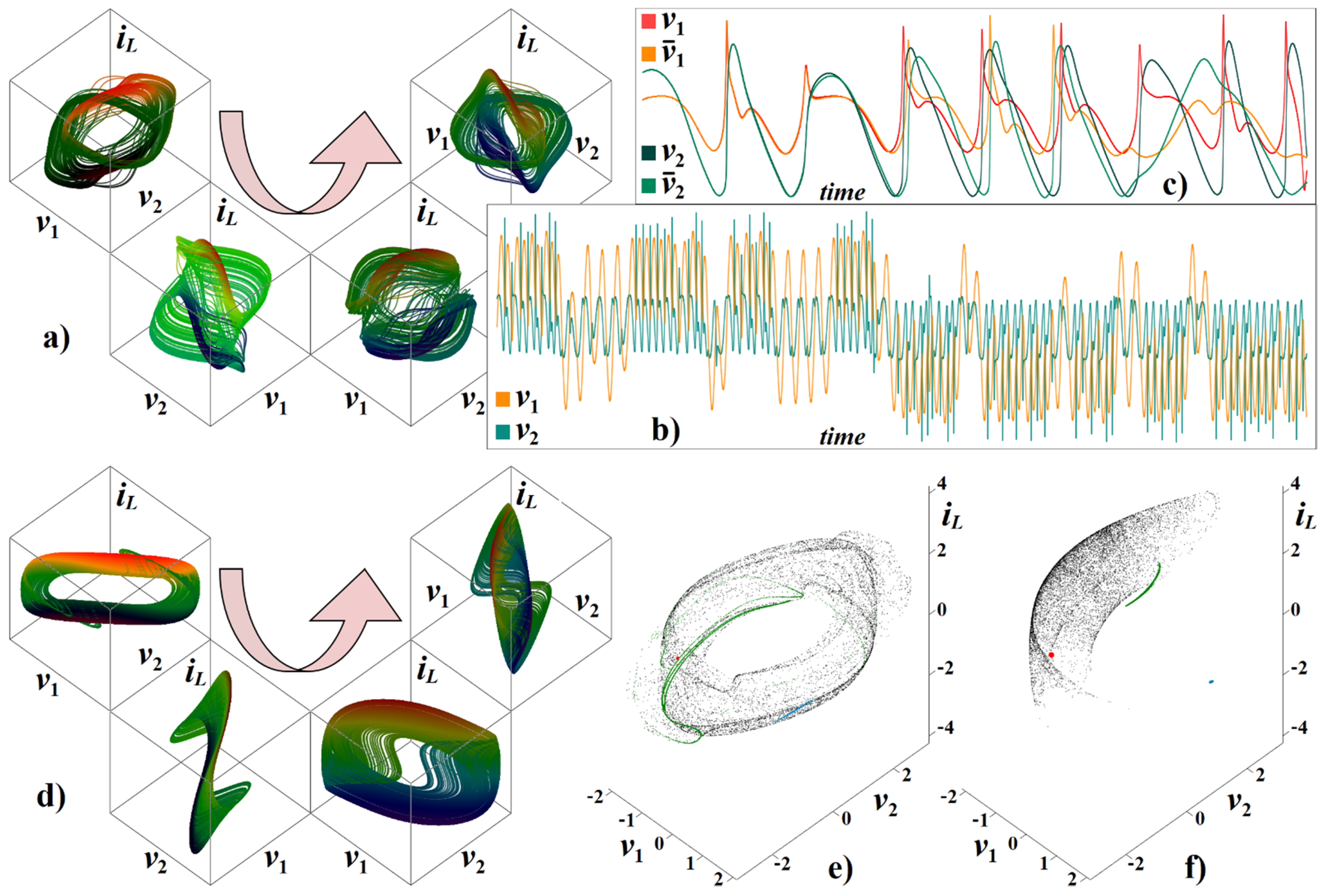
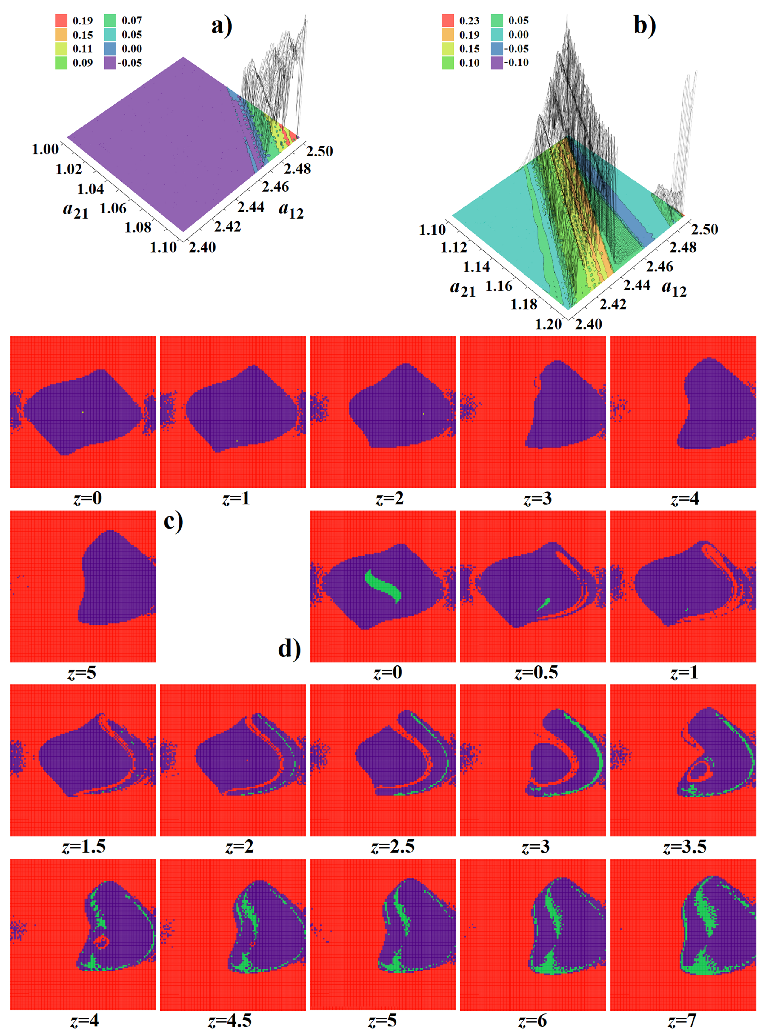
3. Numerical Analysis and Localization of Chaotic Behavior

Assume that the symbolic expression for the mathematical model in the form of system of the first order ordinary differential equations is available. Let us start with numerical values associated with generalized transistor presented in paper [27]. We can put suitable dynamical flow quantifier (calculation of Lyapunov exponents) inside a parallel processing loop in Matlab, create a seventh dimensional hyperspace of internal system parameters using full grid with decimal parameter step, and run repeated calculations. This numerical routine finds chaotic behavior for the several distinct sets of parameters. For both chaotic cases mentioned below, we adopted the additional condition a ¯   =   a ˜ and this choice reduce parameter space investigated by search algorithm by one. This also shrinks possible cases of third order chaotic dynamical systems to those having a single fixed point located at the origin, namely those with a saddle spiral local geometry with a stability index one. Obviously, the fourth order chaotic system possess more equilibrium points including one located at origin.
Firstly, note that all circuit parameters are still defined using normalized values, with respect to both impedance and frequency. Two sets of parameters that lead to the chaotic behavior were discovered for third order dynamical system. The first one is:
y ¯ 11   =   1.0 ,   y ¯ 12   =   2.2 ,   y ¯ 22   =   0.0 ,   a ¯   =   1.0 ,   b ¯   =   1.5 ,   y ˜ 11   =   0.4 ,   y ˜ 12   =   2.0 ,   y ˜ 22   =   0.0 ,   a ˜   =   1.0 ,   b ˜   =   2.0 ,
where line and wavelet sign mean parameter associated with upper and lower transistor respectively (see Figure 1a). The second set can be expressed as:
y ¯ 11   =   0.9 ,   y ¯ 12   =   2.1 ,   y ¯ 22   =   0.0 ,   a ¯   =   1.0 ,   b ¯   =   1.5 , y ˜ 11   =   0.0 ,   y ˜ 12   =   2.0 ,   y ˜ 22   =   0.0 ,   a ˜   =   1.0 ,   b ˜   =   2.0 ,
In the case of fourth-order dynamical system we have one set of internal system parameters that leads to chaotic solution, namely:
y ¯ 11   =   8.0 ,   y ¯ 12   =   1.0 ,   y ¯ 22   =   0.0 ,   a ¯   =   3.0 ,   b ¯   =   2.0 , y ˜ 11   =   0.5 ,   y ˜ 12   =   0.1 ,   y ˜ 22   =   0.0 ,   a ˜   =   3.0 ,   b ˜   =   1.4 ,
Numerically integrated strange attractor obtained by using Mathcad and build-in fourth order Runge-Kutta method and for list of values Equation (7) is demonstrated in Figure 3a. Parameters leading to this result are final time 5000 s with fixed time step 0.1 s and initial conditions x0 = (1, 2, 0)T. Figure 3b shows that same state trajectory plotted with respect of time, time range has linear scale, starts with 0 s and ends with 200 s. Chaotic trajectory evolves accordingly to the spiral repellor located at state (0, 0, 0)T. Figure 3c demonstrates that the analyzed mathematical model exhibits extreme sensitivity of system solution to tiny changes of the initial conditions in the time instance from 0 s to 20 s. The second trajectory is integrated with initial state x0 = (1.01, 2, 0)T. Note that both integrated state trajectories start to significantly differ approximately in the middle of provided time interval, that is after 10 s. Figure 3d provides numerical integration of the state trajectory for parameter set Equation (8) and for initial conditions x0 = (−1, −2, 0)T. Colored three dimensional views are rotated along vertical axis z as indicated by arrow, i.e., along line x = y = 0. Fundamental property of chaos, that is the extreme sensitivity of system solution to the tiny uncertainties of the initial states, is visualized in Figure 3e,f, respectively. Explanation of these plots is following: red dots represent 104 initial states generated with normal distribution (standard deviation 0.01) around point x0 = (−1, −2, 0)T. After a short time of the system evolution (10 s), blue dots are stored, after additional 10 s green dots are placed and finally, after 100 s of system evolution, black dots are placed. Numerical integration was performed using a decreased time step 0.01 s to ensure smooth trajectory evolution and better accuracy.
Figure 4 shows colored projections of the strange attractors generated by fourth order analyzed system into three-dimensional state space subspaces. Three differently shaped dense attractors have been discovered for the same mathematical model, with an exception that one internal parameter has different numerical value. Note that attractors generated by both third order and fourth order dynamical systems exhibit symmetry with respect to horizontal plane z = 0. In addition, dynamical flows are invariant with respect to the coordinate inversion, that is linear transformation (x, y, z)T→(−x, −y, −z)T.
The meaning of the graph of largest Lyapunov exponent (LLE) as function of system parameter is to mark regions (locations and compactness) where system behavior is truly chaotic. Thus, this graph is especially important if parameter space is associated to circuit realization of chaotic oscillator.
d d t ( v 1 v 2 i L )   =   ( a 11 a 12 a 13 a 21 a 22 a 23 a 31 a 32 a 33 ) · ( v 1 v 2 i L )   +   ( f ( v 1 ,   v 2 ) g ( v 1 ,   v 2 ) 0 ) ,
where functions f(.) and g(.) comprises all nonlinear terms. Figure 5a,b represents visualization of LLE as a two-dimensional surface-contour plot with respect to coefficients a21 and a12 in the sense of matrix Equation (10). The type of dynamical motion corresponds to the colored legend provided therein for the largest LE: a value close to zero is limit cycle, positive value indicates chaos and areas with negative value marks fixed point solution. As will be clarified later, both swept coefficients correspond to the variable resistors in the practical circuit realization. During this analysis, final time used for LLE calculation was increased to 104 s with time step 10 ms. Numerical values of system parameters should be adjusted precisely to observe desired strange attractor. Figure 5c,d provide rough specification of basins of attraction for dynamical system Equation (1) with set Equation (7), individual plots represent the horizontal slices of the state space, i.e., planes z = const. Namely, these planes are assumed as z = 0, z = 1, z = 2, z = 3, z = 4, z = 5 for Figure 5c and z = 0, z = 0.5, z = 1, z = 1.5, z = 2, z = 2.5, z = 3, z = 3.5, z = 4, z = 4.5, z = 5, z = 6, and z = 7 for Figure 5d. Basins for the negative values of z coordinate need not be visualized due to the vector field symmetry.
Figure 6 represents contour graphs of first (lower plots) and second (upper plots) LE if these are sorted from the largest to the smallest value, again with respect to the cubic polynomial terms. Color scale for second largest LE is the same as it is for Figure 5. However, positive value of both LEs means that system starts to exhibit the so-called hyperchaotic behavior. In fact, this kind of a very complex motion where the vector field stretches two-dimensional subspace occurs very rarely and is marked by dark red color in upper plots. These are especially visible in parameter space defined by Figure 6a,b,g,h,m,n. Nevertheless, note that areas where analyzed dynamical system exhibit “simple” chaos are wide and continuous.
Figure 7, Figure 8 and Figure 9 provide distribution of kinetic energy over the state space volume where typical strange attractor is evolved. Note that chaotic attractor evolves in regions characterized by low dynamic energy. Individual plots also contain color legend showing energy value normalized to 1 s time instance.

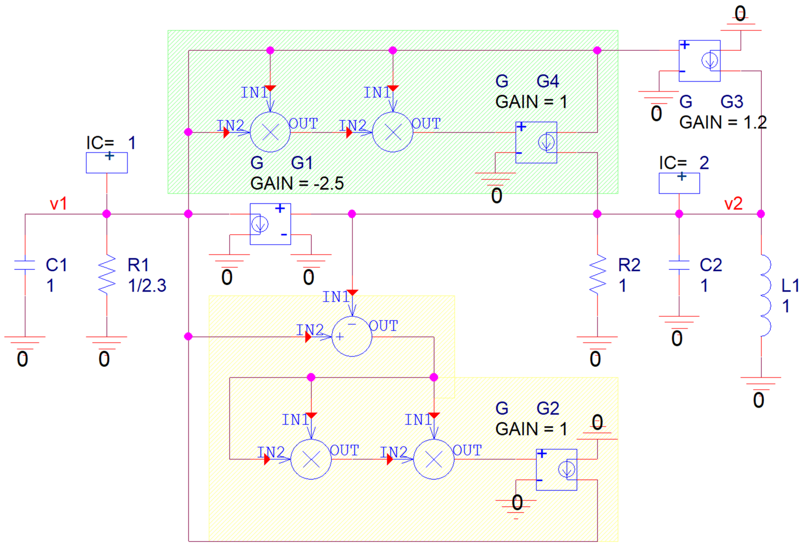
4. Design of Flow-Equivalent Lumped Circuit

Circuit realization followed by experimental verification belongs to mandatory parts in papers where new chaotic system is presented. The reason for this is as follows: if the desired strange attractor captured via oscilloscope is dense and geometrically consistent with that obtained by numerical integration process, we can speak about structural stability and robustness of strange attractor. This proposition should be considered also from the viewpoint of time constant of constructed chaotic oscillator.
The first step toward circuit realization of chaotic oscillator should be computer-aided design and simulation. Of course, software such as Orcad Pspice can treat with both real and normalized numerical values of the circuit components. By considering normalized values, that is those obtained using optimization routine, we can significantly simplify set of the ordinary differential equations of discovered third-order autonomous deterministic dynamical system Equation (1), namely:
d d t v 1   =   2.3 · v 1   +   2.5 · v 2     v 1 3   +   ( v 1     v 2 ) 3 , d d t v 2   =   1.2 · v 1 v 2     i L   +   v 1 3 , d d t i L   =   v 2 ,
where the state vector is x = (v1, v2, iL)T and parameter group Equation (7) is considered. Circuit realization of this system is provided in Figure 10. For the second set of parameters in Equation (8), this mathematical model slightly changes into:
d d t v 1   =   2.7 · v 1   +   2.6 · v 2     v 1 3   +   ( v 1     v 2 ) 3 , d d t v 2   =   v 1     0.9 · v 2     i L   +   v 1 3 , d d t i L   =   v 2 ,
Pseudo-component IC (Initial Condition) serve to inject specific initial conditions into circuit, that is, define nonzero voltage in specific node at time instance 0 s. Note that polynomial forward trans-conductances work as nonlinear current sources controlled by voltages. Highlighted parts represent the nonlinear function v13 (green) and (v1v2)3, respectively. Results of associated time-domain analysis are in Figure 11.
Fourth-order chaotic system can be designed and verified using simulation software on the same level of abstraction, i.e., with ideal controlled sources and multipliers. After substitution of numerical values obtained using a searching procedure mentioned above, we can get following chaotic dynamical system:
d d t v 1   =   0.6 · v 1   +   2 · v 2     0.1 · v 3     3 · v 2 3 , d d t v 2   =   0.3 · v 1     0.1 · v 2     7.9 · v 3   +   3 · v 1 3 , d d t v 3   =   0.1 · v 1   +   0.1 · v 2     0.1 · v 3     i L , d d t i L   =   v 3 ,
where the state vector extends to x = (v1, v2, v3, iL)T and the corresponding circuitry can be found in Figure 12. Few selected time domain simulation results are provided in Figure 13.
However, practical implementation of the real-valued circuitry is of more importance.
Note that fitness function utilized inside multi-criteria optimization procedure for chaos localization can be arranged such that both generalized bipolar transistors have the same equivalent circuit, see principal two-port in Figure 14a. Of course, in such a situation, also real circuitry implementation is exactly the same, as evident from schematic given in Figure 14b. The only difference is in numerical values of admittance parameters. In this schematic, upper index k = 1, 2 represents k-th transistor and ξ is the impedance norm chosen in the beginning stage of design of the chaotic oscillator. Nonlinear forward trans-conductance has the odd-symmetrical saturation-type shape and can be approximated using piecewise-linear function without losing chance to observe chaotic motion.
Chaotic oscillator can be implemented easily if describing differential equations are known. One universal and straightforward approach is known as analog computer and is thoroughly described in many papers, for example [29,30]. The drawback of this method is the necessity to use many active elements. Number of the voltage-feedback operational amplifiers can be subsequently reduced by introducing suitable linear transformation of the coordinates.
The possible practical realization of system Equation (6) is provided in Figure 15 and behavior of this circuit is determined by following set of differential equations:
C d d t v 1   =   1 R 1 v 1   +   1 R 6 v 2     K 2 R 7 v 1 3   +   K 2 R 11 ( R 12 R 8 v 1     R 12 R 9 v 2 ) 3 , C d d t v 2   =   1 R 2 v 1     1 R 3 v 2     1 R 5 v 3   +   K 2 R 10 v 1 3 , C d d t v 3   =   1 R 4 v 2 ,
where K = 0.1 is internally trimmed transfer constant of AD633 and fundamental change of coordinates v1v1, v2 → −v2, iL → −v3 was adopted. Note that values of all capacitors are unified. Now assume that impedance norm is chosen as 104 and the frequency norm as 104. Then, numerical values of the passive components associated with parameter set Equation (7) are as follows: C1 = C2 = C3 = 10 nF, R1 = 4.3 kΩ, R2 = 8.3 kΩ, R3 = 10 kΩ, R4 = 10 kΩ, R5 = 10 kΩ, R6 = 4 kΩ, R7 = 100 Ω, R8 = 10 kΩ, R9 = 10 kΩ, R10 = 100 Ω, R11 = 100 Ω, and R12 = 10 kΩ. To switch the circuit to the second type of behavior defined by parameter group Equation (8), only a few changes in passive components need to be respected: C1 = C2 = C3 = 10 nF, R1 = 3.7 kΩ, R2 = 10 kΩ, R3 = 11 kΩ, R4 = 10 kΩ, R5 = 10 kΩ, R6 = 3.8 kΩ, R7 = 100 Ω, R8 = 10 kΩ, R9 = 10 kΩ, and R10 = 100 Ω, R11 = 100 Ω, R12 = 10 kΩ.
An analogical approach can be applied to design fourth order chaotic dynamical system. The corresponding circuitry is provided in Figure 16 for which following set of ordinary differential equations can be derived:
C d d t v 1   =   1 R 1 v 1   +   R 9 R 10 · 1 R 11 v 2     1 R 8 v 3     K 2 R 14 v 2 3 , C d d t v 2   =   1 R 2 v 1     1 R 3 v 2     1 R 12 v 3   +   K 2 R 13 v 1 3 , C d d t v 3   =   1 R 15 v 1   +   R 9 R 10 · 1 R 4 v 2     1 R 5 v 3     1 R 7 v 4 , C d d t v 4   =   1 R 6 v 3 ,
where transformation of coordinates v1v1, v2v2, v3v3, iLv4 was adopted. Note that values of all capacitors are unified. Now assume that impedance norm is chosen as 104 and frequency norm as 104.
Then, numerical values of the circuit passive components are C1 = C2 = C3 = 10 nF, R1 = 17 kΩ, R2 = 3 kΩ, R3 = 100 kΩ, R4 = 100 kΩ, R5 = 100 kΩ, R6 = 10 kΩ, R7 = 10 kΩ, R8 = 100 kΩ, R9 = 10 kΩ, R10 = 10 kΩ, R11 = 5 kΩ, R12 = 1.3 kΩ, R13 = 33 Ω, R14 = 33 Ω, and R15 = 100 kΩ. Number of active devices does not increase for this higher order chaotic system.

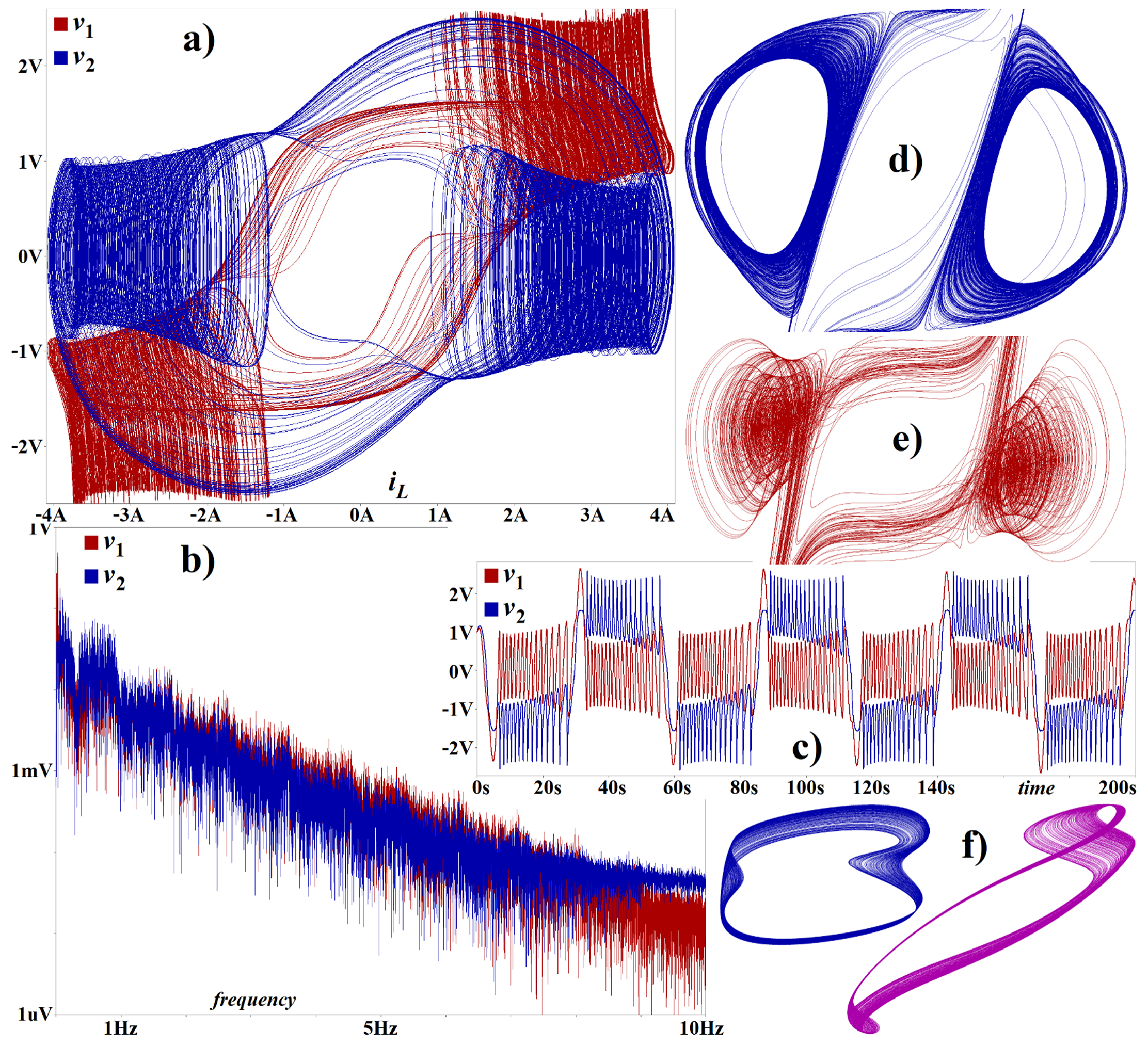
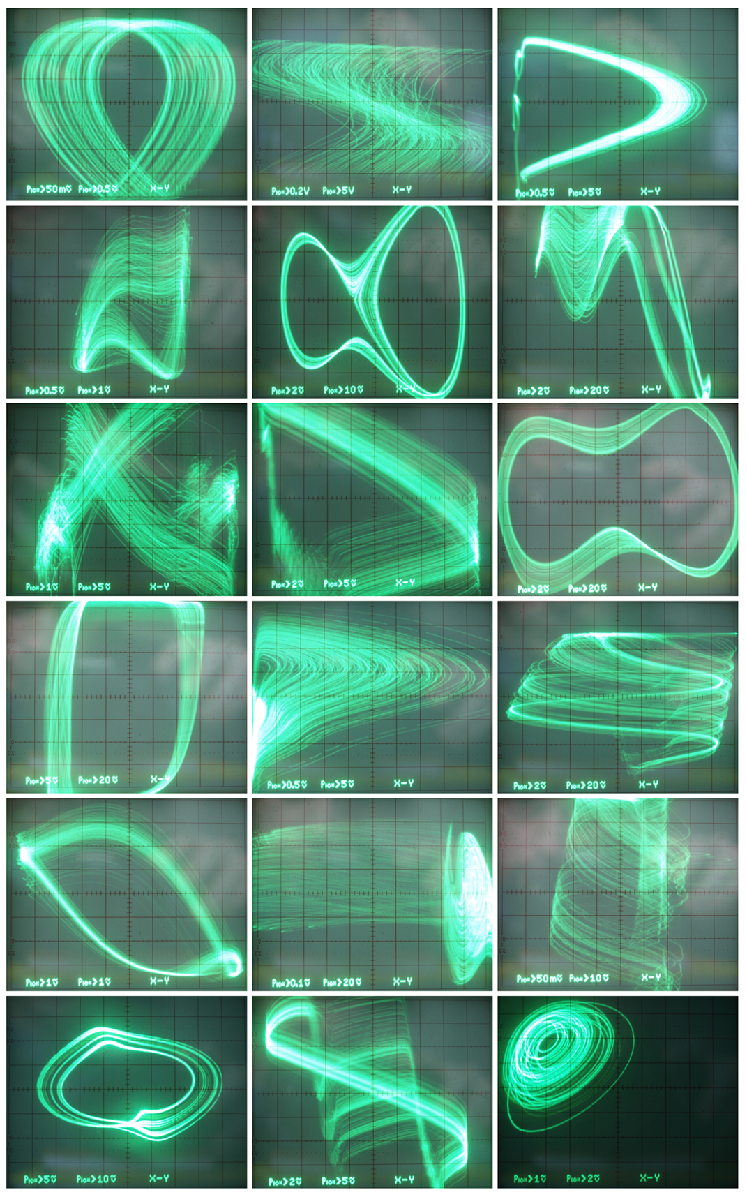
5. Experimental Measurement

All state variables are easily measurable as voltages at the outputs of the inverting integrators. Supply voltage is symmetrical ±15 V, total power dissipation is about 1.35 W. Few selected measurement results for the third-order chaotic oscillator are provided by means of Figure 17. Experimental validation, especially visual validation of the prescribed strange attractors turns to be rather difficult because of the riddled basin of attraction. For the second set of internal parameters Equation (8) entire neighborhood of origin does not belong to the attraction set leading to chaotic attractor. Hand-made injection of the specific initial conditions into proper circuit nodes was tricky and often pushes trajectory to infinity. During measurement, desired strange attractors were affected even by small perturbations of the supply voltage. Observed strange attractors are also very sensitive to precision adjustment of variable resistors. Despite mentioned difficulties, very good agreement with geometrical shapes of numerically integrated trajectories can be pronounced, at least for both groups of internal system parameters Equations (7) and (8). Note that chaotic orbits simulated/calculated by Orcad Pspice and provided in Figure 11c,f can be matched with captured oscilloscope screenshots visualized within Figure 17. Moreover, for the real-valued passive components mentioned above, frequency spectrum of generated chaotic signals is in audio band and bifurcation phenomena can be heard.
Evolution of chaos can be smoothly traced via continuous change of several resistors, for example R1, R2, R3, R5 or R6 (in the case of third-order oscillator) and R1, R2, R3, R5, R8, R12 (for fourth-order chaotic system). One example of circuit-oriented bifurcation scenario is provided by means of Figure 18. Besides chaotic dynamics designed analog oscillator exhibit periodic and quasiperiodic orbits, multi-stability and large limit cycle defined by the saturation levels of the active elements.
In addition to expected chaotic attractors, several interesting geometrical structures of the strange attractors were discovered during experimental investigation and left unnoticed during numerical analysis.

6. Discussion

This paper describes process of chaos-oriented numerical analysis of the well-known configuration of lambda diode. However, common combination of unipolar and bipolar transistor was substituted by a pair of generalized bipolar transistors. As it has been foreseen in paper [27], existence of suitably coupled two such transistors (considered as two-ports with nonlinear forward trans-conductances) can lead to hyperchaotic motion, that is long-time unpredictable behavior with two-dimensional average trajectory expansion. As mentioned in Section 3, positive LE are quite low and restricted to very small regions in space composed by internal system parameters opened for optimization routine. This statement of weak hyperchaos is, of course, related to other, more famous hyperchaotic dynamical systems. Thus, suitability of discovered “new” dynamical system for some practical applications where strong hyperchaos is needed remains questionable and leave the place for further research.
As clarified in text above, circuitry analyzed in this paper is considered isolated, i.e., without driving force in the form of voltage or current waveform. This is in accordance with typical application of lambda diode: compensation of losses in the resonant LC tank. However, both forms of input signal can be easily included into mathematical model Equations (1) and (6). For example, voltage source Vin(t) in series with internal intrinsic resistance Rg can be applied to k-th independent circuit node by adding term [Vin(t) − vk]/Rg where k = 1, 2 for third-order system and k = 1, 2, 3 for fourth-order system. External current sources can be easily added to right-hand side of k-th differential equation of system Equations (1) and (6).
It should be emphasized that analyzed lumped circuit, both third order and fourth order, was willingly forced into the chaotic regime. Thus, various control mechanisms that can circularize [31] generated behavior, control chaotic motion, and/or stabilize amplitude can be considered as interesting problem for future investigation.
Nowadays, fractional-order differential equations that describe chaotic phenomena are addressed instead of integer-order operators. Some papers show that this sort of mathematical generalization can lead to more comprehensive gallery of strange attractors [32]. Doing so, orders close to unity are chosen since low decimal values often exhibit solutions with low geometrical complexity (due to stronger system dissipation). Fractional-order chaotic oscillators can be analyzed purely mathematically [33] or on circuit-level where fractional-order elements are approximated in the frequency domain [34]. Both problems open new areas of future research.
To this end, chaotic attractors discovered and presented in this paper belong to the class of self-excited. Hidden strange attractors remain, exactly in accordance with their names, hidden in full mesh of the initial conditions. Again, addressing this problem and solving of their existence is worthy of analysis.

7. Conclusions

This paper presents thorough numerical analysis of a new hyperchaotic dynamical system and shows its robust fully analog circuitry realization. Transition between chaotic and non-chaotic states (usually limit cycles) can be traced via change of a single resistor. At the same moment, five (Figure 15) or six (Figure 16) variable resistors can be used for this purpose, showing different route-to-chaos scenarios.
In the hyperspace of internal system parameters, regions leading to the robust chaotic behavior are wide, bulky and without significant disruptions, areas that result into hyperchaotic attractors are rather small. Kaplan-Yorke dimension of strange attractor produced by dynamical system Equation (1) with parameter set Equation (7) is about 2.056 and the same system having parameters Equation (8) is 2.105. Numerical value of approximate entropy calculated using algorithm described in paper [35] equals 0.199 for dynamical system Equation (1) with parameter group Equation (7), equals 0.266 for the same system having internal parameters Equation (8), and 0.216 for fourth-order chaotic dynamics. For this analysis 104 time samples of first state variable with time step 0.01 s was utilized. Embedded dimension was chosen in accordance with analyzed dynamical system.
Interconnection of several generalized bipolar transistors necessarily has two immediate consequences: 1. strongly nonlinear vector field, and 2. enough degrees of freedom required for evolution of very complex dynamics. Thus, investigation of other analog functional blocks such as negative resistance, cascode, multi-stage amplifier, and similar structures will probably reveal interesting kind of dynamical motions as well.

Funding

This research was funded by grant agency of Czech Republic, through grant number 19-22248S.

Acknowledgments

Laboratory experiments presented in this paper have been carried out using infrastructure of SIX Centre located at DREL FEEC BUT.

Conflicts of Interest

The author declares no conflict of interest.

References

  1. Matsumoto, T. A chaotic attractor from Chua’s circuit. IEEE Trans. Circuits Syst. 1984, 31, 1055–1058. [Google Scholar] [CrossRef]
  2. Guzan, M. Variations of boundary surface in Chua’s circuit. Radioengineering 2015, 24, 814–823. [Google Scholar] [CrossRef]
  3. Chua, L.O.; Lin, G.-N. Canonical realization of Chua´s circuit family. IEEE Trans. Circuits Syst. 1990, 37, 885–902. [Google Scholar] [CrossRef]
  4. Kilic, R. Experimental study of CFOA-based inductorless Chua´s circuit. Int. J. Bifurc. Chaos 2004, 14, 1369–1374. [Google Scholar] [CrossRef]
  5. Itoh, M. Spread spectrum communication via chaos. Int. J. Bifurc. Chaos 1999, 9, 155–213. [Google Scholar] [CrossRef]
  6. Jafari, S.; Sprott, J.C.; Pham, V.-T.; Golpayegani, S.M.R.Z.; Jafari, A.M. A new cost function for parameter estimation of chaotic systems using return maps as fingerprints. Int. J. Bifurc. Chaos 2014, 24, 1450134. [Google Scholar] [CrossRef]
  7. Petrzela, J. Optimal piecewise-linear approximation of the quadratic chaotic dynamics. Radioengineering 2012, 21, 20–28. [Google Scholar]
  8. Ogorzalek, M.J. Order and chaos in a third-order RC ladder network with nonlinear feedback. IEEE Trans. Circuits Syst. 1989, 36, 1221–1232. [Google Scholar] [CrossRef]
  9. Elwakil, A.S.; Kennedy, M.P. Construction of classes of circuit-independent chaotic oscillators using passive-only nonlinear devices. IEEE Trans. Circuits Syst.-I Fundam. Theory Appl. 2001, 48, 289–307. [Google Scholar] [CrossRef] [Green Version]
  10. Petrzela, J.; Polak, L. Minimal realizations of autonomous chaotic oscillators based on trans-immittance filters. IEEE Access 2019, 7, 17561–17577. [Google Scholar] [CrossRef]
  11. Kilic, R.; Yildrim, F. A survey of Wien bridge-based chaotic oscillators: Design and experimental issues. Chaos Solitons Fractals 2008, 38, 1394–1410. [Google Scholar] [CrossRef]
  12. Rajagopal, K.; Li, C.; Nazarimehr, F.; Karthikeyan, A.; Duraisamy, P.; Jafari, S. Chaotic dynamics of modified Wien bridge oscillator with fractional order memristor. Radioengineering 2019, 28, 165–174. [Google Scholar] [CrossRef]
  13. Kennedy, M.P. Chaos in the Colpitts oscillator. IEEE Trans. Circuits Syst. 1994, 41, 771–774. [Google Scholar] [CrossRef]
  14. Kvarda, P. Chaos in Hartley´s oscillator. Int. J. Bifurc. Chaos 2011, 12, 2229–2232. [Google Scholar]
  15. Yener, S.C.; Kuntman, H.H. Fully CMOS memristor based chaotic circuit. Radioengineering 2014, 23, 1140–1149. [Google Scholar]
  16. Itoh, M. Synthesis of electronic circuits for simulating nonlinear dynamics. Int. J. Bifurc. Chaos 2001, 11, 605–653. [Google Scholar] [CrossRef]
  17. Petrzela, J.; Gotthans, T.; Guzan, M. Current-mode network structures dedicated for simulation of dynamical systems with plane continuum of equilibrium. J. Circuits Syst. Comput. 2018, 27, 1830004. [Google Scholar] [CrossRef]
  18. Pham, V.-T.; Ali, D.S.; Al-Saidi, N.M.G.; Rajagopal, K.; Alsaadi, F.E.; Jafari, S. A novel mega-stable chaotic circuit. Radioengineering 2020, 29, 140–146. [Google Scholar] [CrossRef]
  19. Karimov, T.; Nepomuceno, E.G.; Druzhina, O.; Karimov, A.; Butusov, D. Chaotic oscillators as inductive sensors: Theory and practice. Sensors 2019, 19, 4314. [Google Scholar] [CrossRef] [Green Version]
  20. Petrzela, J. On the existence of chaos in the electronically adjustable structures of the state variable filters. Int. J. Circuit Theory Appl. 2016, 44, 1779–1797. [Google Scholar] [CrossRef]
  21. Endo, T.; Chua, L.O. Chaos from phase-locked loops. IEEE Trans. Circuits Syst. 1988, 35, 987–1003. [Google Scholar] [CrossRef]
  22. Hamill, D.C.; Jeffries, D.J. Subharmonics and chaos in a controlled switched-mode power converter. IEEE Trans. Circuits Syst. 1988, 35, 1059–1061. [Google Scholar] [CrossRef]
  23. Zhou, X.; Li, J.; Youjie, M. Chaos phenomena in dc-dc converter and chaos control. Procedia Eng. 2012, 29, 470–473. [Google Scholar] [CrossRef] [Green Version]
  24. Niu, Q. Study on bifurcation and chaos in boost converter based on energy balance model. Energy Power Eng. 2009, 1, 38–43. [Google Scholar] [CrossRef] [Green Version]
  25. Fossas, E.; Olivar, G. Study of chaos in the buck converter. IEEE Trans. Circuits Syst. I Fund. Theory Appl. 1996, 43, 13–25. [Google Scholar] [CrossRef] [Green Version]
  26. Petrzela, J. Strange attractors generated by multiple-valued static memory cell with polynomial approximation of resonant tunneling diodes. Entropy 2018, 20, 697. [Google Scholar] [CrossRef] [PubMed] [Green Version]
  27. Petrzela, J. New chaotic oscillator derived from class C single transistor-based amplifier. Math. Probl. Eng. 2020, 2640629. [Google Scholar] [CrossRef]
  28. Minati, L.; Frasca, M.; Oswiecimka, P.; Faes, L.; Drozd, S. Atypical transistor-based chaotic oscillators: Design, realization, and diversity. Chaos 2017, 27, 073113. [Google Scholar] [CrossRef] [PubMed]
  29. Kiers, K.; Klein, T.; Kolb, J.; Price, S.; Sprott, J.C. Chaos in a nonlinear analog computer. Int. J. Bifurc. Chaos 2004, 14, 2867–2873. [Google Scholar] [CrossRef]
  30. Gotthans, T.; Petrzela, J. Experimental study of the sampled labyrinth chaos. Radioengineering 2011, 20, 873–879. [Google Scholar]
  31. Cooper, M.; Heidlauf, P.; Sands, T. Controlling chaos—forced van der Pol equation. Mathematics 2017, 5, 70. [Google Scholar] [CrossRef] [Green Version]
  32. Pham, V.-T.; Kingni, S.T.; Volos, C.H.; Jafari, S.; Kapitaniak, T. A simple three-dimensional fractional-order chaotic system without equilibrium: Dynamics, circuitry implementation, chaos control and synchronization. AEU-Int. J. Electron. Commun. 2017, 78, 220–227. [Google Scholar] [CrossRef]
  33. Munoz-Pacheco, J.M.; Zambrano-Serrano, E.; Volos, C.H.; Jafari, S.; Kengne, J.; Rajagopal, K. A new fractional-order chaotic system with different families of hidden and self-excited attractors. Entropy 2018, 20, 564. [Google Scholar] [CrossRef] [PubMed] [Green Version]
  34. Petrzela, J. Fractional-order chaotic memory with wideband constant phase elements. Entropy 2020, 22, 422. [Google Scholar] [CrossRef] [Green Version]
  35. Pinchus, S. Approximate entropy (ApEn) as a complexity measure. Chaos 1995, 5, 110–117. [Google Scholar] [CrossRef] [PubMed]
Figure 1. Negative resistance oscillator with the lambda diode: (a) principal schematic with generalized bipolar transistors, (b) equivalent small-signal model with nonlinear voltage controlled current sources.
Applsci 11 03326 g001
Figure 2. Negative resistance oscillator with a resistor-biased lambda diode: (a) principal schematic considering generalized bipolar transistors, (b) equivalent small-signal model with the nonlinear voltage controlled current sources.
Applsci 11 03326 g002
Figure 3. Numerical analysis of third order dynamical system: (a) 3D plot of the typical strange attractor generated by (1) with parameter set (7), (b) chaotic waveforms in time domain, (c) sensitivity of system solution to small changes of the initial conditions plotted with respect to time, (d) 3D plot of the typical strange attractor generated by (1) with parameter group (8), (e,f) sensitivity of system solution visualized in the state space, see text for details. Ranges for individual state variables in plot (a) are v1∈(−4, 4) V, v2∈(−2, 2) V, and iL∈(−2, 2) A, axis ranges for plot (d) are v1∈(−1, 1) V, v2∈(−2, 2) V, and iL∈(−2, 2) A.
Applsci 11 03326 g003
Figure 4. Typical strange attractors generated by analyzed fourth order dynamical system and visualized using 3D subspaces, different internal parameters of second generalized bipolar transistors, namely: (a) b ˜   =   1.4 , (b) b ˜   =   1 , (c) y ˜ 11   =   0.22 . Ranges for individual state variables are v1∈(−1, 1) V, v2∈(−1, 1) V, v3∈(−100, 100) mV, and iL∈(−100, 100) mA.
Applsci 11 03326 g004
Figure 5. Selected numerical results associated with third order chaotic system: (a,b) rainbow-scaled contour plots of largest Lyapunov exponent (LLE) as two-dimensional functions of the internal parameters of chaotic oscillator, parameter step 0.001, graph contains 10,201 points. Colored basins of attraction for ranges of state variables x∈(−5, 5) and y∈(−5, 5), chaotic solution (red), unbounded solution (red), fixed point (green): (c) dynamical system Equation (1) with parameter group Equation (8), (d) dynamical system Equation (1) having parameter set Equation (8).
Applsci 11 03326 g005
Figure 6. Rainbow-scaled contour plots of LLE as two-dimensional functions of parameters of generalized transistors for fourth order dynamical system: (a) second LE and (b) first LE for parameter range a ˜ ( 2 ,   1 ) , a ¯ ( 2 ,   1 ) , (c) second LE and (d) first LE for parameter range a ˜ ( 3 ,   2 ) , a ¯ ( 2 ,   1 ) , (e) second LE and (f) first LE for parameter range a ˜ ( 4 ,   3 ) , a ¯ ( 2 ,   1 ) , (g) second LE and (h) first LE for parameter range a ˜ ( 2 ,   1 ) , a ¯ ( 3 ,   2 ) , (i) second LE and (j) first LE for parameter range a ˜ ( 3 ,   2 ) , a ¯ ( 3 ,   2 ) , (k) second LE and (l) first LE for parameter range a ˜ ( 4 ,   3 ) , a ¯ ( 3 ,   2 ) , (m) second LE and (n) first LE for parameter range a ˜ ( 2 ,   1 ) , a ¯ ( 4 ,   3 ) , (o) second LE and (p) first LE for parameter range a ˜ ( 3 ,   2 ) , a ¯ ( 4 ,   3 ) , (q) second LE and (r) first LE for parameter range a ˜ ( 4 ,   3 ) , a ¯ ( 4 ,   3 ) . Individual images are plotted for different shapes of forward polynomial trans-conductances.
Applsci 11 03326 g006
Figure 7. Distribution of kinetic energy normalized to final time 1 s over the state space for chaotic attractor generated by the first case of third order system. Poincaré sections (black dots) are taken as the intersections of a state trajectory (white curve) with horizontal planes defined by: (a) z = −3.3, (b) z = −2, (c) z = −1, (d) z = 0.
Applsci 11 03326 g007
Figure 8. Distribution of kinetic energy normalized to final time 1 s over the state space for chaotic attractor generated by the second case of third order system. Poincaré sections (black dots) are taken as intersections of state trajectory (white curve) with horizontal planes defined by: (a) z = −3.3, (b) z = −2, (c) z = −1, (d) z = 0.
Applsci 11 03326 g008
Figure 9. Distribution of kinetic energy normalized to final time 1 s over state space for chaotic attractor generated by fourth order system. Poincaré sections (black dots) are the intersections of a state trajectory (white curve) with horizontal planes defined by the following relations: (a) z = −0.1, (b) z = −0.08, (c) z = −0.05, (d) z = 0.
Applsci 11 03326 g009
Figure 10. Maximally idealized third-order dynamical system, circuit realization using pseudo-components MULT (multiplication of two input voltages) and voltage-controlled current-sources G.
Applsci 11 03326 g010
Figure 11. Maximally idealized third-order dynamical system, selected Orcad Pspice simulation results: (a) plane projections v1 vs. iL and v2 vs. iL, (b) baseband frequency spectrum of the generated signal v1 and v2, (c) chaotic signals v1 and v2 plotted with respect to time, (df) plane projections of interesting strange attractors (slightly modified nominal set of system parameters).
Applsci 11 03326 g011
Figure 12. Orcad Pspice simulation results for idealized fourth-order system, circuit realization using pseudo-components MULT and voltage-controlled current-sources G.
Applsci 11 03326 g012
Figure 13. Idealized fourth-order system, selected Orcad Pspice simulation results: (a) signals v1 and v2 in time domain, (b) plane projections v1 vs. iL and v2 vs. iL, (c) baseband frequency spectrum of the generated signal v1 and v2, (d) plane projection v2 vs. v1, (e) plane projection v3 vs. v1.
Applsci 11 03326 g013
Figure 14. Generalized bipolar transistor designed based on optimization: (a) two-port equivalent network, (b) active circuitry implementation using commercially available integrated circuits.
Applsci 11 03326 g014
Figure 15. Third order autonomous analog chaotic oscillator using cheap and off-the-shelf active elements, namely single TL084, one AD844 and four AD633.
Applsci 11 03326 g015
Figure 16. Fourth order fully analog chaotic oscillator constructed by using only commercially available active elements, namely single TL084, one AD844 and four AD633.
Applsci 11 03326 g016
Figure 17. Experimental confirmation of strange attractors in oscillator defined by Equation (13).
Applsci 11 03326 g017
Figure 18. Bifurcation scenarios plotted as two-dimensional projections of state orbit visualized for dynamical system Equation (1) with parameter group Equation (8) via small changes of a variable resistor R1 (black), R2 (red), and R3 (blue).
Applsci 11 03326 g018
Publisher’s Note: MDPI stays neutral with regard to jurisdictional claims in published maps and institutional affiliations.

