Article

Effects of Thermal Annealing on the Characteristics of High Frequency FBAR Devices

1
Department of Electrical Engineering, National Sun Yat-sen University, Kaohsiung 80424, Taiwan
2
Medical Devices and Opto-Electronics Equipment Department, Metal Industries Research and Development Center, Kaohsiung 811, Taiwan
3
Department of Electronic Engineering, HungKuo Delin University of Technology, New Taipei 236, Taiwan
*
Author to whom correspondence should be addressed.
Coatings 2021, 11(4), 397; https://doi.org/10.3390/coatings11040397
Submission received: 28 February 2021 / Revised: 26 March 2021 / Accepted: 29 March 2021 / Published: 30 March 2021
(This article belongs to the Special Issue Selected Papers from the IIKII 2020&2021 Conferences)

Abstract

:
In this study, piezoelectric zinc oxide (ZnO) thin film was deposited on the Pt/Ti/SiNx/Si substrate to construct the FBAR device. The Pt/Ti multilayers were deposited on SiNx/Si as the bottom electrode and the Al thin film was deposited on the ZnO piezoelectric layer as the top electrode by a DC sputtering system. The ZnO thin film was deposited onto the Pt thin film by a radio frequency (RF) magnetron sputtering system. The cavity on back side for acoustic reflection of the FBAR device was achieved by KOH solution and reactive ion etching (RIE) processes. The crystalline structures and surface morphologies of the films were analyzed by X-ray diffraction (XRD) and field emission scanning electron microscope (FE-SEM). The optimized as-deposited ZnO thin films with preferred (002)-orientation were obtained under the sputtering power of 80 W and sputtering pressure of 20 mTorr. The crystalline characteristics of ZnO thin films and the frequency responses of the FBAR devices can be improved by using the rapid thermal annealing (RTA) process. The optimized annealing temperature and annealing time are 400 °C and 10 min, respectively. Finally, the FBAR devices with structure of Al/ZnO/Pt/Ti/SiNx/Si were fabricated. The frequency responses showed that the return loss of the FBAR device with RTA annealing was improved from −24.07 to −34.66 dB, and the electromechanical coupling coefficient (kt2) was improved from 1.73% to 3.02% with the resonance frequency of around 3.4 GHz.

1. Introduction

In recent years, the development of wireless communication systems is toward high frequency band and high stability, in which, the acoustic devices used in the systems must be small size, low cost and high stability [1,2]. The film bulk acoustic resonators (FBARs) existed lower insertion loss, higher operating frequency and wider frequency band which were better than those of surface acoustic wave (SAW) devices [3,4,5,6,7]. The FBAR device is constructed by a piezoelectric layer sandwiched between the top and bottom electrodes. The frequency responses of FBAR devices would be affected by the piezoelectric materials, thicknesses of piezoelectric and electrode materials and their qualities. In order to increase the resonance frequency of an FBAR device, the thickness of the piezoelectric layer should be decreased, which would result in the deterioration of the characteristics of the piezoelectric film and decrease the electromechanical coupling coefficient of the FBAR device. Hence, the precise thickness with optimized characteristics of the piezoelectric layer is strict for high frequency FBAR devices.
Some novel materials can be used in acoustic wave devices, such as, GaN, AlGaN, ScGaN and ScAlN [8,9,10]. In general, zinc oxide (ZnO) and aluminum nitride (AlN) thin films are commonly used in acoustic wave devices [11,12,13,14,15,16,17,18,19,20]. The lead zirconate titanate (PZT) thin films are not adopted due to their impacts on the environment. The ZnO thin films have a wide bandgap of 3.37 eV at room temperature, a high excitation binding energy of about 60 meV, high acoustic wave velocity, high electromechanical coupling coefficient, strong bonding, high chemical stability, easy acquisition and low cost [21,22,23]. The ZnO thin films can be grown at room temperature with a columnar structure and pebble-like surface morphologies with low roughness [24]. Therefore, zinc oxide is suitable for the fabrication of thin film bulk acoustic wave devices. In general, the rapid thermal annealing (RTA) process is adopted to improve the characteristics of as-deposited films because the processing time is short, and the qualities of films are better than those obtained by conventional annealing process with the furnace tube [25,26]. It has been approved that the qualities of piezoelectric thin films, the optical properties, the sensitivities and responses of the SAW UV sensors after the RAT process have been significantly improved [27,28,29]. Therefore, it is expected that the characteristics of piezoelectric ZnO thin films and the frequency responses of FBAR devices can be improved through the treatment of the RTA process.
In this study, it was focused on the fabrication of FBAR devices with resonance frequency of about 3.4–3.6 GHz for 5G wireless communication systems. The FBAR device was constructed by an acoustic cavity on the back side of the substrate, ZnO thin films, and electrode thin films. The bottom Pt/Ti and top Al electrode thin films were fabricated on the SiNx/Si substrate and piezoelectric layer, respectively, by a DC sputtering system. The ZnO piezoelectric layer was deposited on the bottom electrode by a radio frequency (RF) magnetron sputtering system. Finally, the as-deposited ZnO thin films and fabricated FBAR devices were annealed by RTA with various temperatures and times. The effects of rapid thermal annealing process on the crystalline characteristics of ZnO thin films and the frequency responses of FBAR devices were investigated and discussed.

2. Materials and Methods
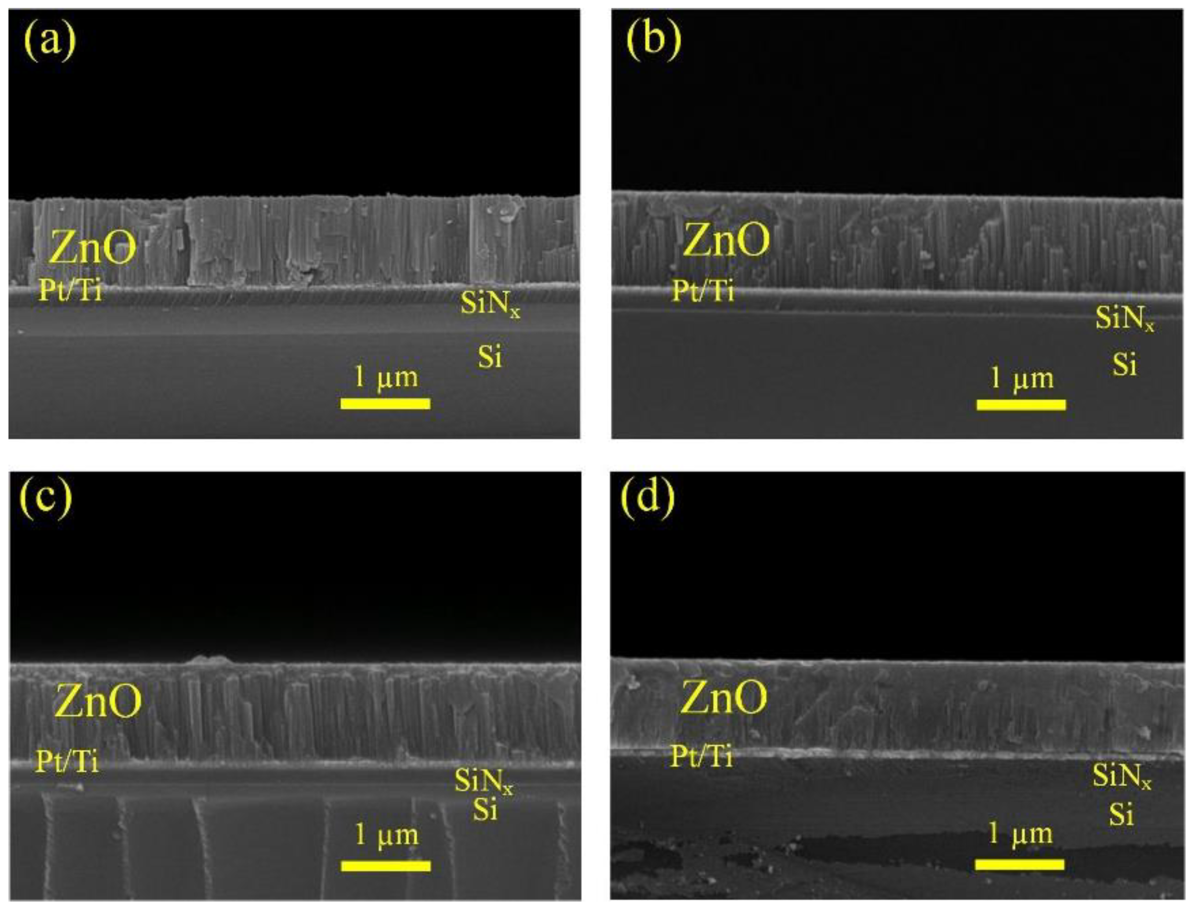
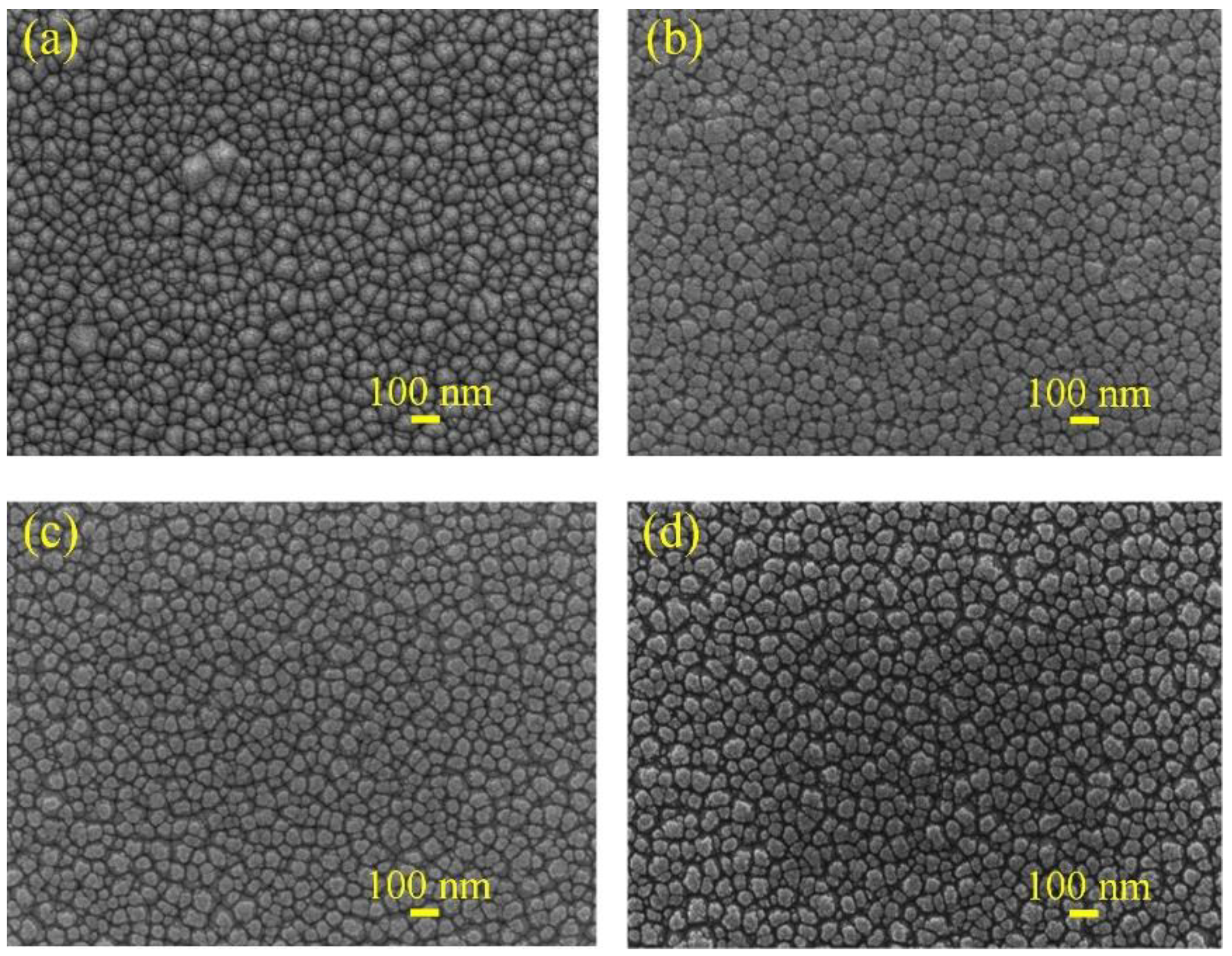
A schematic of fabrication processes of an FBAR device is shown in Figure 1. The structure of an FBAR device consisted a piezoelectric layer sandwiched between top and bottom electrodes, and a substrate with an acoustic cavity on back side. The SiNx thin films were deposited on both sides of Si substrates by a low pressure chemical vapor deposition (LPCVD) system. The back-sided SiNx film was patterned and etched to define the acoustic cavity area of the FBAR device by the reactive ion etching processes (RIE, United Kingdom STS Company, Newport, MODEL C001-4). The Pt/Ti multilayers were deposited on the SiNx/Si substrate as the bottom electrode and Al was deposited on the piezoelectric layer as the top electrode, respectively, by a DC sputtering system. In the bottom electrode, Ti is adopted as an adhesion layer between Pt and SiNx/Si substrate. The deposition parameters are shown in Table 1. The piezoelectric ZnO thin film was deposited by a RF magnetron sputtering system. The deposition parameters are shown in Table 2. The acoustic cavity on back side of the substrate was achieved by a 30 wt % KOH etching solution at 100 °C followed by the RIE processes. The RTA apparatus (ULVAC, MILA-3000, Kanagawa, Japan) with infrared concentrated heater at atmosphere was adopted for the annealing of ZnO thin films. The annealing parameters are shown in Table 3. Finally, the obtained FBAR devices were annealed using the optimized annealing parameters for ZnO thin films.
The preferred orientation and crystalline characteristics of ZnO thin films were analyzed by XRD (Bruker D8 Advance, Billerica, MA, USA) with CuKα radiation. The surface morphologies and cross-sectional images of ZnO thin films were analyzed by SEM (JEOL JSM-6700F, Tokyo, Japan). The thickness of ZnO thin film for the FBAR device was derived through the formula v = f × 2 d , in which, v is the bulk acoustic wave velocity of ZnO thin film, f is the center frequency of resonance, and 2d is the thickness of ZnO thin film. The frequency responses of FBAR devices were measured by a network analyzer (E5071C) and a CASCADE high frequency probe station.

3. Results

A preliminary investigation was carried out in this study to obtain the ZnO thin films with highly c-axis orientation and uniform surface morphologies by a RF magnetron sputtering system. The optimized as-deposited ZnO thin films were obtained under the sputtering power of 80 W and sputtering pressure of 20 mTorr at room temperature. In order to improve the qualities of ZnO thin films, the effects of various RTA temperatures and times on the ZnO thin films were analyzed by XRD measurements, as shown in Figure 2 and Figure 3.
The XRD patterns showed that all the ZnO thin films were c-axis orientation, and the peaks of (002) crystalline phase of ZnO thin films increase with RTA time and RTA temperature. The reasons may due to the strain, the density and distribution of defects in ZnO thin films are reduced as the annealing temperature and time increases [30]. The optimized RTA temperature and RTA time were 400 °C and 10 min, respectively. As the annealing temperature increased above 400 °C, the micro-cracks and agglomeration of grains were observed, as described below, which resulted in the deterioration of the columnar structures of (002) crystallization of ZnO films. In addition, the grain sizes of ZnO thin films were calculated from the XRD patterns using Scherrer’s formula as follows [31,32]:
D = k λ β cos θ
where k is the shape factor of about 0.9, λ is the wavelength of radiation of X-ray, β is the full width at half maximum (FWHM) and 2θ is the diffraction angle of the (002) crystalline the FBAR phase in the X-ray patterns. Table 4 and Table 5 show the grain sizes and FWHM of the ZnO thin films with various RTA times and RTA temperatures, respectively. It can be observed that as the temperature increased, the FWHM decreased and grain size increased, which indicates that the film quality was improved. Although the quality of ZnO thin film annealed at 500 °C appeared to be superior to that of annealed at 400 °C, as compared in Table 4, the intensity of XRD pattern showed that the one annealed at 400 °C was much better than that annealed at 500 °C, as shown in Figure 2. Therefore, the annealing temperature of the ZnO thin films was chosen as 400 °C. From Table 5, the lowest FWHM value was found at 10 min, in which, the average grain size was larger than others. It also exhibited better crystalline characteristics as compared with XRD patterns, as shown in Figure 3. From the results, the optimized crystalline characteristics and the c-axis preferred orientation of ZnO thin films were obtained as the RTA temperature was 400 °C and RTA time was 10 min.
The surface morphologies and cross-sectional images of as-deposited and RTA treated ZnO thin films were analyzed by SEM, as shown in Figure 4, Figure 5, Figure 6 and Figure 7. The uniform pebble-like surface morphologies and columnar structures of c-axis orientation are presented for both as-deposited and RTA treated ZnO thin films. The surface morphologies of ZnO thin films became uniform and smooth as the annealing temperature and time increased, as shown in Figure 4 and Figure 6. Although the residual stress in the thin films would be decreased as the RTA temperature increased, the films existed micro-cracks on the surfaces and the grains began to agglomerate and the columnar structure gradually deteriorated as the annealing temperature reached 500 °C, as shown in Figure 4d and Figure 5d. These phenomena will also result in a reduction of acoustic wave velocity [29].
In order to compare the frequency responses of FBAR devices with and without RTA annealing, the fabricated FBAR devices with the thickness of ZnO thin films of about 770 nm were subjected to the RTA annealing process with annealing temperature of 400 °C and annealing time of 10 min. The thickness of about 770 nm was desired to meet the 5G wireless communication systems with resonance frequency of about 3.4–3.6 GHz. The frequency responses of the FBAR devices with and without RTA annealing were shown in Figure 8. The resonance frequencies were near 3.4 GHz for both devices, whereas the FBAR device without RTA annealing exhibited a poor return loss (S11) of −24.07 dB, comparing to that of −34.66 dB for the device with RTA annealing. The FBAR device without RTA annealing exhibited an acoustic wave velocity of 5245 m/s, comparing to that of 5219 m/s for the FBAR device with RTA annealing. The results showed that the return loss was improved significantly, while the acoustic wave velocity decreased slightly, which may be due to the some or less surface cracks as mentioned above [29]. The stress and defects in the zinc oxide film may be reduced for the FBAR device with RTA annealing, so that the device exhibited better piezoelectric conversion performance, and the return loss of the device was improved. These results were similar to those derived on SAW UV sensor proposed by Phan, D.T., etc., in that, the sensitivity and response of the SAW UV sensor after RTA thermal annealing are greatly improved [27].
The electromechanical coupling coefficient (kt2) of an FBAR device can be calculated as follows:
k t 2 = tan = ( π 2 ) ( f s f p ) tan ( ( π 2 ) ( f s f p ) ) ( π 2 ) 2 ( f p f s f p )
in which, fs is the series resonance frequency and fp is the parallel resonance frequency [33]. The electromechanical coupling coefficient of the FBAR device without RTA annealing was about 1.73%, whereas, it was about 3.02% for the annealed one. From the results obtained above, it showed that the characteristics of high frequency FBAR devices could be improved by RTA thermal annealing process.
Table 6 shows the performance parameters of FBAR related devices with ZnO films as the piezoelectric layers in the literatures. It shows that the electromechanical coupling coefficients (kt2) were within 3%~5% except the SMR and HBAR devices. Additionally, it could be find that with lower resonance frequency, the FBAR device exhibited higher kt2. The reason may be attributed to the lower the resonance frequency of the FBAR device, the thicker the ZnO film is needed, and the better crystalline characteristics of ZnO film can be achieved, which will result in higher kt2 values.

4. Conclusions

In this study, the optimized parameters for the deposition of ZnO thin films were obtained with sputtering power of 80 W, sputtering pressure of 20 mTorr and gas ratio of 75% (O2/O2+N2), respectively. The as-deposited ZnO thin films existed a preferred c-axis (002) orientation, and the grain size was consistent with the obtained characteristics from the XRD and SEM analyses. The optimized characteristics of ZnO thin films could be achieved by the RTA process under annealing temperature of 400 °C and annealing time of 10 min. Finally, the FBAR devices with structure of Al/ZnO (770 nm)/Pt/Ti/SiNx/Si were fabricated and subjected to the RTA annealing process with annealing temperature of 400 °C and annealing time of 10 min. The frequency responses showed that the return loss of the FBAR device with RTA annealing was improved from −24.07 to −34.66 dB, and the electromechanical coupling coefficient was improved from 1.73% to 3.02% with the resonance frequency of around 3.4 GHz.

Author Contributions

Data curation, Y.-C.C. (Yu-Chen Chang), Y.-C.C. (Ying-Chung Chen), B.-R.L., W.-C.S., J.-M.L., W.-T.C. and C.-C.C.; Formal analysis, Y.-C.C. and B.-R.L.; Writing—original draft preparation, Y.-C.C. (Yu-Chen Chang) and Y.-C.C. (Ying-Chung Chen); Writing—review and editing, Y.-C.C. (Ying-Chung Chen), W.-T.C. and C.-C.C. All authors have read and agreed to the published version of the manuscript.

Funding

This research received no external funding.

Institutional Review Board Statement

Not applicable.

Informed Consent Statement

Not applicable.

Data Availability Statement

Not applicable.

Acknowledgments

The authors gratefully acknowledge financial support from the Ministry of Science and Technology, Taiwan, R.O.C. under contract nos. 103-2221-E-110-075-MY2, 105-2221-E-110-074-MY2 and Industrial Development Bureau, Ministry of Economic Affairs, Medical Devices and Opto-Electronics Equipment Department.

Conflicts of Interest

The authors declare no conflict of interest.

References

  1. Nolan, P.; Auer, S.; Spehar, A.; Oplatowska-Stachowiak, M.; Campbell, K. Evaluation of mass sensitive micro-array biosensors for their feasibility in multiplex detection of low molecular weight toxins using mycotoxins as model compounds. Talanta 2021, 222, 1–12. [Google Scholar] [CrossRef] [PubMed]
  2. Wang, L.; Lin, A.; Kim, E.S. Miniature sensing system with FBAR-based oscillators and frequency shift detector. IEEE Sens. J. 2018, 18, 7633–7637. [Google Scholar] [CrossRef]
  3. Zhao, J.H.; Xing, Y.H.; Han, J.; Lin, W.K.; Yun, X.F.; Sun, Y.H.; Zhou, X.; Wang, Z.M.; Cao, X.; Zhang, B.S.; et al. The research of dual-mode film bulk acoustic resonator for enhancing temperature sensitivity. Semicond. Sci. Technol. 2021, 36, 1–8. [Google Scholar] [CrossRef]
  4. Ruby, R.C.; Radley, P.B.; Shmyansky, Y.O.; Chien, A.; Larson, J.D., III. Thin film bulk wave acoustic resonator (FBAR) for wireless applications. In Proceedings of the IEEE Ultrasonics Symposium. Proceedings. An International Symposium, San Juan, PR, USA, 22–25 October 2000; pp. 813–821. [Google Scholar]
  5. Afzal, A.; Iqbal, N.; Mujahid, A.; Schirhagl, R. Advanced vapor recognition materials for selective and fast responsive surface acoustic wave sensors: A review. Anal. Chim. Acta 2013, 787, 36–49. [Google Scholar] [CrossRef]
  6. Serhane, R.; Abdelli-Messaci, S.; Lafane, S.; Khales, H.; Aouimeur, W.; Hassein-Bey, A.; Boutkedjirt, T. Pulsed laser deposition of piezoelectric ZnO thin films for bulk acoustic wave devices. Appl. Surf. Sci. 2014, 288, 572–578. [Google Scholar] [CrossRef]
  7. Zhang, X.; Xu, W.C.; Chae, J. Temperature effects on a high Q FBAR in liquid. Sens. Actuator A Phys. 2011, 166, 264–268. [Google Scholar] [CrossRef]
  8. Shealy, J.B.; Hodge, M.D.; Patel, P.; Vetury, R.; Feldman, A.Y.; Gibb, S.R.; Boomgarden, M.D.; Lewis, M.P.; Shealy, J.B.; Shealy, J.R. Single crystal AlGaN bulk acoustic wave resonators on silicon substrates with high electromechanical coupling. In Proceedings of the IEEE Radio Frequency Integrated Circuits Symposium (RFIC), San Francisco, CA, USA, 22–24 May 2016; pp. 103–106. [Google Scholar]
  9. Uehara, M.; Mizuno, T.; Aida, Y.; Yamada, H.; Umeda, K.; Akiyama, M. Increase in the piezoelectric response of scandium-doped gallium nitride thin films sputtered using a metal interlayer for piezo MEMS. Appl. Phys. Lett. 2019, 114, 1–5. [Google Scholar] [CrossRef]
  10. Schneider, M.; DeMiguel-Ramos, M.; Flewitt, A.J.; Iborra, E.; Schmid, U. Scandium aluminum nitride-based film bulk acoustic resonators. Proceedings 2017, 1, 305. [Google Scholar] [CrossRef] [Green Version]
  11. Wei, C.L.; Chen, Y.C.; Li, S.R.; Cheng, C.C.; Kao, K.S.; Chung, C.J. Effects of reflecting layers on resonance characteristics of a solidly mounted resonator with 1/4 𝜆 mode configuration. Appl. Phys. A 2010, 99, 271–278. [Google Scholar] [CrossRef]
  12. Chen, Y.C.; Chang, W.T.; Kao, K.S.; Yang, C.H.; Cheng, C.C. The liquid sensor using thin film bulk acoustic resonator with c-axis tilted AlN films. J. Nanomater. 2013, 2013, 245095. [Google Scholar] [CrossRef]
  13. Sharma, G.; Liljeholm, L.; Enlund, J.; Bjurstrom, J.; Katardjiev, I.; Hjort, K. Fabrication and characterization of a shear mode AlN solidly mounted resonator-silicone microfluidic system for in-liquid sensor applications. Sens. Actuator A Phys. 2010, 159, 111–116. [Google Scholar] [CrossRef]
  14. Mirea, T.; Clement, M.; Olivares, J.; Iborra, E. Assessment of the absolute mass attachment to an AlN-based solidly mounted resonator using a single shear mode. IEEE Electron Device Lett. 2020, 41, 609–612. [Google Scholar] [CrossRef]
  15. Qin, L.F.; Chen, Q.M.; Cheng, H.B.; Wang, Q.M. Analytical study of dual-mode thin film bulk acoustic resonators (FBARs) based on ZnO and AlN films with tilted c-axis orientation. IEEE Trans. Ultrason. Ferroelectr. Freq. Control 2010, 57, 1840–1853. [Google Scholar] [PubMed]
  16. Sun, P.; Chen, Y.R.; Tang, T.T.; Shen, J.; Liu, X.; Yang, X.M.; Gao, C. Effect of c-axis tilted orientation ZnO thin film on shear-mode bulk acoustic resonator in liquid environment. Mater. Express 2020, 10, 1477–1483. [Google Scholar] [CrossRef]
  17. Yu, L.; Jin, H.; Hu, N.; Dong, S.; Luo, J. Flexible film bulk acoustic resonators and filter-like structure made directly on polymer substrates. Integr. Ferroelectr. 2016, 168, 157–162. [Google Scholar] [CrossRef]
  18. Patel, R.; Bansal, D.; Agrawal, V.K.; Rangra, K.; Boolchandani, D. Fabrication and RF characterization of zinc oxide based film bulk acoustic resonator. Superlattices Microstruct. 2018, 118, 104–115. [Google Scholar] [CrossRef]
  19. Corso, C.D.; Dickherber, A.; Hunt, W.D.; Corso, C.D. Lateral field excitation of thickness shear mode waves in a thin film ZnO solidly mounted resonator. J. Appl. Phys. 2007, 101, 1–7. [Google Scholar] [CrossRef]
  20. Liu, M.W.; Zhu, M.B.; Li, J.H.; Wang, C.H. High Q, high frequency, high overtone bulk acoustic resonator with ZnO films. J. Zhejiang Univ. Sci. C 2013, 14, 279–282. [Google Scholar] [CrossRef]
  21. Ali, A.I.; Ammar, A.H.; Abdel Moez, A. Influence of substrate temperature on structural, optical properties and dielectric results of nano-ZnO thin films prepared by Radio Frequency technique. Superlattices Microstruct. 2014, 65, 285–298. [Google Scholar] [CrossRef]
  22. Sharma, S.; Vyas, S.; Periasamy, C.; Chakrabarti, P. Structural and optical characterization of ZnO thin films for optoelectronic device applications by RF sputtering technique. Superlattices Microstruct. 2014, 75, 378–389. [Google Scholar] [CrossRef]
  23. Varma, T.; Periasamy, C.; Boolchandani, D. Performance evaluation of bottom gate ZnO based thin film transistors with different W/L ratios for UV sensing. Superlattices Microstruct. 2018, 114, 284–295. [Google Scholar] [CrossRef]
  24. Park, S.H.; Seo, B.C.; Park, H.D.; Yoon, G. Film bulk acoustic resonator fabrication for radio frequency filter applications. Jpn. J. Appl. Phys. 2000, 39, 4115–4119. [Google Scholar] [CrossRef]
  25. Lee, Y.C.; Hu, S.Y.; Water, W.; Tiong, K.K.; Feng, Z.C.; Chen, Y.T.; Huang, J.C.; Lee, J.W.; Huang, C.C.; Shen, J.L.; et al. Rapid thermal annealing effects on the structural and optical properties of ZnO films deposited on Si substrates. J. Lumin. 2009, 129, 148–152. [Google Scholar] [CrossRef]
  26. Ma, T.Y.; Shim, D.K. Effects of rapid thermal annealing on the morphology and electrical properties of ZnO/In films. Thin Solid Films 2002, 410, 8–13. [Google Scholar] [CrossRef]
  27. Wang, W.B.; Gu, H.; He, X.L.; Xuan, W.P.; Chen, J.K.; Wang, X.Z.; Luo, J.K. Thermal annealing effect on ZnO surface acoustic wave-based ultraviolet light sensors on glass substrates. Appl. Phys. Lett. 2014, 104, 1–4. [Google Scholar] [CrossRef] [Green Version]
  28. Phan, D.T.; Chung, G.S. Effects of rapid thermal annealing on surface acoustic wave ultraviolet sensors using ZnO nanorods grown on AlN/Si structures. J. Electroceram. 2013, 30, 185–190. [Google Scholar] [CrossRef]
  29. Phan, D.T.; Chung, G.S. The effect of geometry and post-annealing on surface acoustic wave characteristics of AlN thin films prepared by magnetron sputtering. Appl. Surf. Sci. 2011, 257, 8696–8701. [Google Scholar] [CrossRef]
  30. Puchert, M.K.; Timbrell, P.Y.; Lamb, R.N. Postdeposition annealing of radio frequency magnetron sputtered ZnO films. J. Vac. Sci. Technol. B 1996, 14, 2220–2230. [Google Scholar] [CrossRef]
  31. Devi, V.; Kumar, M.; Shukla, D.K.; Choudhary, R.J.; Phase, D.M.; Kumar, R.; Joshi, B.C. Structural, optical and electronic structure studies of Al doped ZnO thin films. Superlattices Microstruct. 2015, 83, 431–438. [Google Scholar] [CrossRef]
  32. Nagayasamy, N.; Gandhimathination, S.; Veerasamy, V. The effect of ZnO thin film and its structural and optical properties prepared by Sol-Gel spin coating method. Open J. Met. 2013, 3, 8–11. [Google Scholar] [CrossRef] [Green Version]
  33. Hara, M.; Kuypers, J.; Abe, T.; Esashi, M. Surface micromachined AlN thin film 2 GHz resonator for CMOS integration. Sens. Actuator A Phys. 2005, 117, 211–216. [Google Scholar] [CrossRef]
Figure 1. The fabrication processes of an FBAR device.
Coatings 11 00397 g001
Figure 2. XRD patterns of the ZnO thin films annealed with various temperatures for 10 min.
Coatings 11 00397 g002
Figure 3. XRD patterns of the ZnO thin films annealed at 400 °C with various times.
Coatings 11 00397 g003
Figure 4. The surface morphologies of as-deposited (a) and RTA treated ((b) 300 °C, (c) 400 °C and (d) 500 °C) ZnO thin films for 10 min.
Coatings 11 00397 g004
Figure 5. The cross-sectional images of as-deposited (a) and RTA treated ((b) 300 °C, (c) 400 °C and (d) 500 °C) ZnO thin films for 10 min.
Coatings 11 00397 g005
Figure 6. The surface morphologies of as-deposited (a) and RTA treated ((b) 5 min, (c) 10 min and (d) 15 min) ZnO thin films at 400 °C.
Coatings 11 00397 g006
Figure 7. The cross-sectional images of as-deposited (a) and RTA treated ((b) 5 min, (c) 10 min and (d) 15 min) ZnO thin films at 400 °C.
Coatings 11 00397 g007
Figure 8. The frequency responses of FBAR devices with and without RTA annealing.
Coatings 11 00397 g008
Table 1. Deposition parameters of the bottom and top electrodes.
DC Sputtering System
Target (2 inch)Ti (99.995%)Pt (99.95%)Al (99.999%)
SubstrateSiNx/SiTi/SiNx/SiZnO/Pt/Ti/SiNx/Si
Base pressure (Torr)<5 × 10⁻⁶<5 × 10⁻⁶<5 × 10⁻⁶
Working pressure (mTorr)311
Sputtering power (W)75175100
Substrate temperature (°C)R. T.R. T.R. T.
Ar flow (sccm)101010
Thickness (nm)12100100
Table 2. Deposition parameters of the ZnO thin films.
RF Magnetron Sputtering System
Target (2 inch)Zn (99.999%)
SubstratePt/Ti/SiNx/Si
Base pressure (Torr)<1 × 10⁻⁶
Working pressure (mTorr)20
Sputtering power (W)80
Substrate temperature (°C)R. T.
O2/(O2 + Ar) (%)75
Table 3. RTA annealing parameters of the ZnO thin films.
Annealing time (min)5, 10, 15
Annealing temperature (°C)300, 400, 500
Table 4. Grain sizes and FWHMs of the ZnO thin films annealed at various temperatures for 10 min.
RTA Temperature (°C)Grain Size (nm)FWHM (°)
As-deposited360.24
300360.24
400390.21
500410.20
Table 5. Grain sizes and FWHMs of the ZnO thin films annealed at 400 °C with various times.
RTA Time (min)Grain Size (nm)FWHM (°)
As-deposited360.24
5380.22
10390.21
15350.24
Table 6. The performance parameters of FBAR/HBAR/SMR devices with ZnO thin films.
References[17][18][19][20]This Work
DeviceFBARFBARSMRHBARFBAR
Piezoelectric layerZnOZnOZnOZnOZnO
Frequency (GHz)1.1881.752.21.49/2.43/3.403.38
k t 2 (%)4.74.1540.40.0385/0.0953/0.04793.02
Publisher’s Note: MDPI stays neutral with regard to jurisdictional claims in published maps and institutional affiliations.

